R3200x SERIES
Reset Timer IC for Mobile Equipments
NO.EA-280-190531
OUTLINE
The R3200x is a reset timer IC with two input signals for mobile equipment which require long interval for
reset sequence. The long interval prevents unexpected resets caused by accidental key operations. Internally,
the R3200x consists of a delay generator circuit and output driver transistors.
The R3200x has two active-low input pins (SR0 and SR1) which generate reset signals after output delay time
when both active-low input pins are activated at the same time.
The R3200x has two versions that are different in output delay time settings and output release method.
R3200x001x:
Output delay time is selectable from 7.5 s or 11.25 s typ. by connecting the DSR pin to either GND or VDD. A
reset signal can be released by making one of the active-low input pins high.
R3200xxx2x, R3200L053B or R3200L064A:
Output delay time is fixed. A reset signal will be released automatically after output release time. Or, by
making one of the active-low input pins high, a reset signal can be released before output release time.
The R3200x provides ultra-low supply current while a reset signal is remaining active or after being sent out.
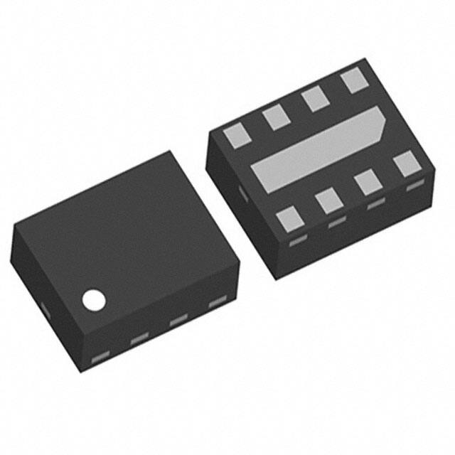
The R3200x is offered in a 8-pin DFN(PLP)2020-8B package or a 8-pin DFN1216-8 package.
1
�R3200x
NO.EA-280-190531
FEATURES
Operating Voltage Range (Maximum Rating).................... 1.65 V to 5.5 V (6 V)
Supply Current 1 (at standby) ........................................... Typ. 0.28 µA (VDD = 5.5 V)
Supply Current 2 (at active before reset signal output) ..... Typ. 3 µA(VDD = 5.5 V)*1
Supply Current 3 (at active after reset signal output) ........ Typ. 0.45 µA (VDD = 5.5 V)
Operating Temperature Range.......................................... −40 to +85°C
Output Delay Time (R3200x001x) ..................................... Typ. 7.5 s or 11.25 s
(R3200x002x) .................................... Typ. 7.5 s
(R3200L052B) .................................... Typ. 10 s
(R3200L053B) ....................................... Typ. 10 s
(R3200L064A) ........................................ Typ. 3.0 s
Output Delay Time Accuracy .................................................. ±10%
Output Release Time (R3200x002x) ...................................... Typ. 0.234 s
(R3200L052B) ...................................... Typ. 0.313 s
(R3200L053B) ...................................... Typ. 0.078 s
(R3200L064A) ................................... Typ. 0.1875 s
Output Release Time Accuracy ......................................... ±10%
Output Type (R3200xxxxA) ............................................... Nch Open Drain
(R3200xxxxB) ............................................... Nch Open Drain and CMOS
Packages .......................................................................... DFN(PLP)2020-8B, DFN1216-8
*1
Guaranteed by design engineering
APPLICATIONS
Mobile phone, Smartphone
Tablet devices such as E-book etc.
Portable Games
Personal Navigation Devices
2
�R3200x
NO.EA-280-190531
BLOCK DIAGRAMS
SR0
VDD
Reset
Logic
*1
Delay Time
Selector
Delay
Logic
RST
OSC
GND
SR1
*1
DSR
Delay Time
Selector
R3200xxxxA
*1
VDD
Reset
Logic
RST2
SR1
DSR
SR0
Delay
Logic
RST
OSC
GND
R3200xxxxB
The parts surrounded by red dotted lines are for the R3200x001x only.
SELECTION GUIDE
The package type, the combination of output delay time and output release time, the output type for the
device are user-selectable options.
Selection Guide
Product Name
Package
Quantity per Reel
Pb Free
Halogen Free
R3200Kxxx-TR
DFN(PLP)2020-8B
5,000 pcs
Yes
Yes
R3200Lxxx-E2
DFN1216-8
5,000 pcs
Yes
Yes
xxx: Specify the combination of output delay time and output release method.
(001) Select the output delay time from 7.5 s or 11.25 s typ.
A reset signal can be released by making one of the active-low input pins high.
(xx2) / (053) / (064)
A reset signal will be released automatically after output release time.
A reset signal can be released before output release time by making one of the active-low input
pins high.
Refer to the table below for the output delay time and the output release time for each device.
002
052 (R3200L052B only)
053 (R3200L053B only)
064 (R3200L064A only)
Output Delay Time
7.5 s
10 s
10 s
3.0 s
Output Release Time
0.234 s
0.313 s
0.078 s
0.1875 s
: Specify the output type.
(A) Nch Open Drain
(B) Nch Open Drain and CMOS
3
�R3200x
NO.EA-280-190531
PIN DESCRIPTIONS
Top View
8
7
6
Top View
Bottom View
5
5
6
7
8
8
7
6
Bottom View
5
5
1
2
3
4
4
6
7
8
3
2
1
3
2
1
1
2
3
4
4
DFN1216-8
DFN(PLP)2020-8B
The tab on the bottom of the package enhances thermal performance and is electrically connected to GND (substrate
level). It is recommended that the tab be connected to the ground plane on the board, or otherwise be left floating.
DFN(PLP)2020-8B Pin Description/ DFN1216-8 Pin Description
Pin No.
1
NC
Description
No Connection (R3200xxxxA)
RST2
CMOS Output Pin, Active-high (R3200xxxxB)
2
GND
Ground Pin
3
SR1
Input Pin2, Active-low*1
4
RST
Nch Open Drain Output Pin, Active-low*2
DSR
Output Delay Time Selection Pin (R3200x001x) (GND: 7.5 s, VDD: 11.25 s)*3
5
*1
Symbol
TEST2
Test Pin 2*4 (R3200xxx2x/ R3200L053B/ R3200L064A)
6
TEST
Test Pin*4
7
SR0
Input Pin1, Active-low*1
8
VDD
Power Supply Input Pin
When only one active-low input pin is used, connect the unused one to GND.
The RST pin must be connected to GND or left floating if it is not used (Ex.R3200xxxxB).
*3
The DSR pin must be connected to GND or VDD.
*4
The TEST pin and the TEST2 pin must be connected to GND when they are used.
*2
4
�R3200x
NO.EA-280-190531
ABSOLUTE MAXIMUM RATINGS
Absolute Maximum Ratings
Symbol
Item
Rating
Unit
VDD
Supply Voltage
GND −0.3 to 6
V
VSR0
Input Voltage (Input Pin1)
GND −0.3 to 6
V
VSR1
Input Voltage (Input Pin2)
GND −0.3 to 6
V
VRST
Output Voltage (Reset Signal Output Pin1)
GND −0.3 to 6
V
VRST2
Output Voltage (Reset Signal Output Pin2)
GND −0.3 to VDD +0.3
V
VDSR
Input Voltage (Output Delay Time Selection Pin)
(R3200x001x)
GND −0.3 to 6
V
IOUT
Output Current
20
mA
PD
Power Dissipation (JEDEC STD. 51)*1
Ta
Operating Temperature Range
−40 to +85
°C
Storage Temperature Range
−55 to +125
°C
Tstg
*1
DFN(PLP)2020-8B
1050
DFN1216-8
1700
mW
Refer to PACKAGE INFORMATION for detailed information.
ABSOLUTE MAXIMUM RATINGS
Electronic and mechanical stress momentarily exceeded absolute maximum ratings may cause permanent damage and
may degrade the life time and safety for both device and system using the device in the field. The functional operation at
or over these absolute maximum ratings is not assured.
RECOMMENDED OPERATING CONDITIONS (ELECTRICAL CHARACTERISTICS)
All of electronic equipment should be designed that the mounted semiconductor devices operate within the
recommended operating conditions. The semiconductor devices cannot operate normally over the recommended
operating conditions, even if they are used over such conditions by momentary electronic noise or surge. And the
semiconductor devices may receive serious damage when they continue to operate over the recommended operating
conditions.
5
�R3200x
NO.EA-280-190531
ELECTRICAL CHARACTERISTICS
The specifications surrounded by
R3200x001x Electrical Characteristics
Symbol
Item
VDD
(Ta = 25°C)
Conditions
Supply Voltage
Min.
Typ.
1.65
*1
ISS1
Supply Current 1
ISS2
Supply Current 2*2
ISS3
Supply Current 3*3
VOL
"L" Output Voltage
VOH
are guaranteed by design engineering at 40C Ta 85C.
VDD = 5.5 V (at standby)
VDD = 5.5 V
(at active before reset signal output)
VDD = 5.5 V
(at active after reset signal output)
VDD ≥ 4.5 V
IOL = 8 mA
*4
"H" Output Voltage
VDD ≥ 3.3 V
IOL = 5 mA
VDD ≥ 1.65 V
IOL = 3 mA
VDD ≥ 4.5 V
IOH = 5 mA
VDD ≥ 3.3 V
IOH = 2.5 mA
VDD ≥ 1.65 V
IOH = 0.8 mA
Max.
Unit
5.5
0.28
1.35
V
µA
3.0
6.5
µA
0.45
1.7
µA
0.3
V
VDD
x 0.85
V
ILEAKI
S R 0 , S R 1 Input
Leakage Current
VDD = 5.5 V
0.1
µA
ILEAKO
Output Leakage Current
VDD = 5.5 V
0.1
µA
tdelay
Output Delay Time
8.25
s
VIL
S R 0 , S R 1 "L" Input Voltaget
VIH
S R 0 , S R 1 "H" Input Voltaget
DSR = GND
DSR = VDD
6.75
7.5
10.125 11.25 12.375
0.3
0.85
s
V
V
All test items listed under ELECTRICAL CHARACTERISTICS are done under the pulse load condition (Tj ≈ Ta = 25°C)
except Supply Current 2.
*1
Supply current when the device is active and waiting for the reset input.
*2
Supply current when both active-low input pins are low and the timer operation is running.
*3
Supply current after the completion of timer operation and the output of reset signal.
*4
For the R3200xxxxB only (CMOS output).
6
�R3200x
NO.EA-280-190531
ELECTRICAL CHARACTERISTICS (continued)
are guaranteed by design engineering at 40°C Ta 85°C.
The specifications surrounded by
R3200xxx2x, R3200L053B, R3200L064A Electrical Characteristics
Symbol
Item
Conditions
VDD
Operating Voltage
ISS1
*1
Supply Current 2*2
ISS3
Supply Current 3*3
VOL
VOH
VDD = 5.5 V (at standby)
VDD = 5.5 V
(at active before reset signal
output)
VDD = 5.5 V
(at active after reset signal output)
"L" Output Voltage
*4
"H" Output Voltage
VDD ≥ 4.5 V
IOL = 8 mA
VDD ≥ 3.3 V
IOL = 5 mA
VDD ≥ 1.65 V
IOL = 3 mA
VDD ≥ 4.5 V
IOH = 5 mA
VDD ≥ 3.3 V
IOH = 2.5 mA
VDD ≥ 1.65 V
IOH = 0.8 mA
ILEAKI
S R 0 , S R 1 Input
Leakage Current
VDD = 5.5 V
ILEAKO
Output Leakage Current
VDD = 5.5 V
tdelay
Typ.
Max.
Unit
5.5
V
0.28
1.35
µA
3.0
6.5
µA
0.45
1.7
µA
0.3
V
1.65
Supply Current 1
ISS2
(Ta = 25°C)
Min.
VDD
x 0.85
V
0.1
µA
0.1
µA
tdelay_s
tdelay_s
tdelay_s
x 0.9
x 1.1
Output Delay Time*5
trec_s
x 0.9
trec
Output Release Time*5
VIL
S R 0 , S R 1 "L" Input Voltage
VIH
S R 0 , S R 1 "H" Input Voltage
0.85
trec_s
sec
trec_s
x 1.1
sec
0.3
V
V
All test items listed under ELECTRICAL CHARACTERISTICS are done under the pulse load condition (Tj ≈ Ta = 25°C)
except Supply Current 2.
*1
Supply current when the device is active and waiting for the reset input.
*2
Supply current when both active-low input pins are low and the timer operation is running.
*3
Supply current after the automatic cancellation of reset signal following the completion of timer operation and the output of rest signal.
*4
For the R3200xxxxB only (CMOS output).
*5
Refer to Output Delay Time and Output Release Time of R3200x.
Output Delay Time and Output Release Time of R3200x
Product Name
tdelay_s
trec_s
R3200x002x
7.5 s
0.234 s
R3200L052B
10 s
0.313 s
R3200L053B
10 s
0.078 s
R3200L064A
3.0 s
0.1875 s
7
�R3200x
NO.EA-280-190531
TYPICAL APPLICATIONS
Power Supply
C
VDD
VDD
CPU
470k
DSR/TEST2
R3200xxxxA
TEST
RESET
RST
SR0
SR1
Power On
GND
GND
Power
Switch
R3200xxxxA Typical Application
Power Supply
C
VDD
Regulator
CE
DSR/TEST2
R3200xxxxB
TEST
RST
SR0
RST2
SR1
GND
Power
Switch
System Power
Output
VDD
CPU
RESET
Power On0
Power On1
GND
Power
Switch
R3200xxxxB Typical Application
A bypass capacitor between the power supply line and the GND line is not necessarily required. If the device operation
is affected by power supply noise, connect an appropriately selected bypass capacitor.
8
�R3200x
NO.EA-280-190531
TECHNICAL NOTES
The performance of power source circuits using this device largely depends on the peripheral circuits. When
selecting the peripheral components, consider the conditions of use. Do not allow each component, PCB
pattern and the device to exceed their respected rated values (voltage, current and power) when designing
the peripheral circuits.
When only one active-low input pins is used (refer to R3200xxxxA Typical Application) connect the
unused one to GND.
In the case of applying the following circuit configuration to the R3200x, the supply current of the device
itself may cause significant voltage drop on the VDD pin if the R1 value is high. As a result, the VDD voltage
may fall below the minimum operating voltage.
Power Supply
R1
RST2
VDD
GND
RST
Circuit Configuration Example
9
�R3200x
NO.EA-280-190531
THEORY OF OPERATION
VDD
1.65V
Timer Timer
Start Stop
Timer
Start
Timer
End
VSR0
tDELAY
VSR1
VRST
VRST2*1
*1
Reset
Reset off
Reset
Reset off
For R3200xxxxB only.
R3200x001x Timing Chart
When both active-low input pins become the low voltage level, the timer operation starts. After the output
delay time (tdelay), a reset signal will be sent out. When one of the active-low input pins becomes the
high voltage level, the timer operation stops.
During tdealy, if one of the active-low input pins becomes the high voltage level, the timer operation stops.
If both active-low input pins become the low voltage level again, a reset signal will be sent out after
tdelay.
A reset signal will be released if one of the active-low input pins becomes the high voltage level. Until one
of the active-low input pins becomes the high voltage level, a reset signal will be continually sent out.
tdelay can be selected from 7.5 s or 11.25 s typ. by connecting the DSR pin to either GND or VDD.
However, if the DSR pin is switched during the operations, the output would become unstable and may
cause false operations. Switching of the DSR pin must be done during power-off.
Also, the DSR pin must be connected to either GND or VDD, otherwise the output would become unstable
and may cause false operations.
10
�R3200x
NO.EA-280-190531
VDD
1.65V
Timer Start
Timer Start
Timer Stop
Timer Start
Timer End
Timer End
VSR0
tDELAY
VSR1
tDELAY
Reset
*1
VRST
Reset
VRST2*1
Reset
tREC
Reset off
Reset off
Reset
Reset off
tREC
Reset off
For R3200xxxxB only.
R3200xxx2x, R3200L053B, R3200L064A Timing Chart
When both active-low input pins become the low voltage level, the timer operation starts. After the output
delay time (tdelay), a reset signal will be sent out. If one of the active-low input pins becomes the high
voltage level, the timer operation stops.
During tdelay, if one of the active-low input pins becomes the high voltage level, the timer operation stops.
If both active-low input pins become the low voltage level again, a reset signal will be sent out after
tdelay.
A reset signal will be released automatically after the reset delay time (trec), or it will be released if one of
the active-low input pins becomes the high voltage level.
11
�R3200x
NO.EA-280-190531
OUTPUT DELAY TIME GAP
The threshold voltages of the active-low input pins are between VIL and VIH. Therefore, if the rising or falling
slew rate is very slow, the timer will start at the point of crossing the threshold voltage and may cause errors in
the output delay time (tdelay) and the output release time (trec).
VIH=0.85V
VDET_H
VSR0, VSR1
VDET_L
VIL=0.3V
Output Delay
Time Gap
VRST
Released Reset
Time Gap
Output Delay
Time
Relation between the Rising and Falling Slew Rate and the Time Gap
VDD START-UP DURING LOW INPUT
When starting up VDD at slow slew rate of 0.001 V/µs or less while the active-low input pins are the low voltage
level, the device may start the operation at lower than the minimum operating voltage, thus tdelay may exceed
the guaranteed time.
12
�R3200x
NO.EA-280-190531
PACKAGE INFORMATION
Power Dissipation (DFN(PLP)2020-8B)
The power dissipation of the package is dependent on PCB material, layout, and environmental conditions.
The following measurement conditions are based on JEDEC STD. 51-7.
Measurement Conditions
Item
Measurement Conditions
Environment
Mounting on Board (Wind Velocity = 0 m/s)
Board Material
Glass Cloth Epoxy Plastic (Four-Layer Board)
Board Dimensions
76.2 mm × 114.3 mm × 0.8 mm
Outer Layer (First Layer): Less than 95% of 50 mm Square
Inner Layers (Second and Third Layers): Approx. 100% of 50 mm Square
Outer Layer (Fourth Layer): Approx. 100% of 50 mm Square
Copper Ratio
0.3 mm × 23 pcs
Through-holes
Measurement Result
Item
(Ta = 25°C, Tjmax = 125°C)
Measurement Result
Power Dissipation
1050 mW
Thermal Resistance (ja)
ja = 92°C/W
Thermal Characterization Parameter (ψjt)
ψjt = 60°C/W
ja: Junction-to-Ambient Thermal Resistance
ψjt: Junction-to-Top Thermal Characterization Parameter
Power Dissipation vs. Ambient Temperature
Measurement Board Pattern
13
�R3200x
NO.EA-280-190531
1.30.05
B
2.00
5
8
0.350.05
A
0.550.05
PACKAGE DIMENSIONS (DFN(PLP)2020-8B)
X4
2.00
0.05
C0.05
INDEX
4
1
0.5
0.6max
0.200.05
Bottom View
0.05min
S
0.05 S
0.05 M AB
(Unit: mm)
The tab on the bottom of the package enhances thermal performance
and is electrically connected to GND (substrate level).
It is recommended that the tab be connected to the ground plane on
the board, or otherwise be left floating.
DFN(PLP)2020-8B Package Dimensions
MARK SPECIFICATION (DFN(PLP)2020-8B)
: Product Code … Refer to MARK SPECIFICATION TABLE (DFN(PLP)2020-8B).
: Lot Number … Alphanumeric Serial Number
8
7
6
5
1
2
3
4
DFN(PLP)2020-8B Mark Specification
14
�R3200x
NO.EA-280-190531
MARK SPECIFICATION TABLE (DFN(PLP)2020-8B)
R3200K Mark Specification Table
Product Name
R3200K001A
R3200K001B
R3200K002A
R3200K002B
D001
DD02
DD03
DD04
15
�R3200x
NO.EA-280-190531
Power Dissipation (DFN1216-8)
The power dissipation of the package is dependent on PCB material, layout, and environmental conditions.
The following conditions are based on JEDEC STD. 51-7.
Measurement Conditions
Item
Measurement Conditions
Environment
Mounting on Board (Wind Velocity = 0 m/s)
Board Material
Glass Cloth Epoxy Plastic (Four-Layer Board)
Board Dimensions
Copper Ratio
76.2 mm × 114.3 mm × 0.8 mm
Outer Layer (First Layer): Less than 95% of 50 mm Square
Inner Layers (Second and Third Layers): Approx. 100% of 50 mm Square
Outer Layer (Fourth Layer): Approx. 100% of 50 mm Square
0.2 mm × 15 pcs
Through-holes
Measurement Result
Item
Power Dissipation
(Ta = 25°C, Tjmax = 125°C)
Measurement Result
1700 mW
Thermal Resistance (ja)
ja = 56°C/W
Thermal Characterization Parameter (ψjt)
ψjt = 18°C/W
ja: Junction-to-Ambient Thermal Resistance
ψjt: Junction-to-Top Thermal Characterization Parameter
Power Dissipation vs. Ambient Temperature
16
Measurement Board Pattern
�R3200x
NO.EA-280-190531
B
X4
1.300.05
5
8
1.20
0.05
0.300.05
C0.15
4
1
0.40
0.4max
INDEX
0.200.05
1.60
0.180.05
Bottom View
0.05
A
0.200.05
PACKAGE DIMENSIONS (DFN1216-8)
0.05
M
AB
(Unit: mm)
0.05 S
S
The tab on the bottom of the package enhances thermal performance
and is electrically connected to GND (substrate level).
It is recommended that the tab be connected to the ground plane on
the board, or otherwise be left floating.
DFN1216-8 Package Dimensions
MARK SPECIFICATION (DFN1216-8)
: Product Code … Refer to MARK SPECIFICATION TABLE (DFN1216-8).
: Lot Number … Alphanumeric Serial Number
DFN1216-8 Mark Specification
17
�R3200x
NO.EA-280-190531
MARK SPECIFICATION TABLE (DFN1216-8)
R3200L Mark Specification Table
Product Name
R3200L001A
R3200L001B
R3200L002A
R3200L002B
R3200L052B
R3200L053B
R3200L064A
18
DE01
DF02
DE03
DE04
DE05
DE06
DE07
�R3200x
NO.EA-280-190531
TEST CIRCUITS
ISS1
RST2
VDD
GND
SR0
SR1
TEST
RST2
VDD
GND
SR0
SR1
TEST
RST
DSR/TEST2
RST
DSR/TEST2
470kΩ
Supply Current Test Circuit
RST2
VDD
GND
SR0
SR1
TEST
RST
DSR/TEST2
VOL
Output Delay Time Test Circuit
VOH
IOUT
RST2
VDD
GND
SR0
SR1
TEST
RST
DSR/TEST2
IOUT
Nch Driver Output Voltage Test Circuit
CMOS Driver Output Voltage Test Circuit
(For the R3200xxxxB only.)
19
�R3200x
NO.EA-280-190531
TYPICAL CHARACTERISTICS
Note: Typical Characteristics are intended to be used as reference data; they are not guaranteed.
1) Supply Current 1 vs. Temperature
R3200x (at standby)
2) Supply Current 2 vs. Temperature
R3200x (before the reset signal output)
4
VDD=5.5V
VDD=5.5V
VDD=3.3V
VDD=3.3V
Supply Current ISS2 (uA)
Supply Current ISS1 (uA)
0.6
VDD=1.65V
0.4
0.2
VDD=1.65V
3
2
1
0
-50
-25
0
25
50
75
Temperature Topt (゜C)
100
3) Supply Current 3 vs. Temperature
R3200x (after the reset signal output)
-50
Supply Current ISS1 (uA)
Supply Current ISS3 (uA)
100
0.6
Topt = 85℃
Topr = 25℃
Topt = -40℃
VDD=5.5V
VDD=3.3V
0.6
VDD=1.65V
0.4
0.2
0.4
0.2
0
0
-50
-25
0
25
50
75
Temperature Topt (゜C)
1
100
5) Supply Current 2 vs. Supply Voltage
R3200x (before the reset signal output)
Supply Current ISS3 (uA)
0.9
3
2
Topt = 85℃
Topr = 25℃
2
3
4
5
Supply Voltage VDD (V)
6
6) Supply Current 2 vs. Supply Voltage
R3200x (after the reset signal output)
4
Supply Current ISS2 (uA)
0
25
50
75
Temperature Topt (゜C)
4) Supply Current 1 vs. Supply Voltage
R3200x (at standby)
0.8
Topt = 85℃
Topr = 25℃
Topt = -40℃
0.6
0.3
Topt = -40 ℃
1
0
1
20
-25
2
3
4
5
Supply Voltage VDD (V)
6
1
2
3
4
Supply Voltage VDD (V)
5
6
�R3200x
NO.EA-280-190531
7) Output Delay Time vs. Temperature
7.7
R3200x001x
R3200x001x
DSR = GND (tdelay: Typ. 7.5 s)
DSR = VDD (tdelay: Typ. 11.25 s)
11.50
VDD=5.5V
Reset Delay Time t DELAY (s)
Reset Delay Time t DELAY (s)
VDD=5.5V
VDD=3.3V
7.6
VDD=1.65V
7.5
7.4
7.3
VDD=3.3V
11.35
VDD=1.65V
11.20
11.05
10.90
-50
-25
0
25
50
Temperature Ta (゜C)
75
100
-50
-25
0
25
50
Temperature Ta (゜C)
75
100
8) Output Release Time vs. Temperature
R3200x002x
R3200x002x
0.245
7.7
Reset Release Time t REC (s)
Reset Delay Time t DELAY (s)
VDD=5.5V
VDD=3.3V
VDD=1.65V
7.6
7.5
7.4
VDD=5.5V
VDD=3.3V
0.240
VDD=1.65V
0.235
0.230
0.225
7.3
-50
-25
0
25
50
75
Temperature Topt (゜C)
-50
100
-25
0
25
50
75
Temperature Topt (゜C)
100
9) Output Delay Time vs. Supply Voltage
R3200x001x
R3200x001x
DSR = GND (tdelay: Typ. 7.0
7.7
DSR = VDD (tdelay: Typ. 11.25 s)
11.50
Reset Delay time t DELAY (s)
Reset Delay Time t DELAY (s)
Topt = -40℃
Topt = 25℃
7.6
Topt = 85℃
7.5
7.4
11.35
11.20
Topt = -40℃
11.05
Topt = 25℃
Topt = 85℃
10.90
7.3
1
2
3
4
5
Supply Voltage VDD (V)
6
1
2
3
4
5
Supply Voltage VDD (V)
6
21
�R3200x
NO.EA-280-190531
10) Output Release Time vs. Supply Voltage
R3200x002x
R3200x002x
0.240
Reset Release Time t REC (s)
Reset Delay Time t DELAY (s)
7.7
7.6
7.5
Topt = 85℃
7.4
Topt = 25℃
Topt = -40℃
7.3
1
2
3
4
5
Supply Voltage VDD (V)
0.235
0.230
Topt = 25℃
Topt = -40℃
0.220
6
1
11) Nch Driver Output Current vs. Supply Voltage
VDS = 0.3 V
Output Current IOUT (mA)
72
16
12
8
Topt = -40℃
Topt = 25℃
4
Topt = 85℃
0
1
2
3
4
5
2
3
4
5
Supply Voltage VDD (V)
VDD=5.5V
VDD=4.5V
VDD=3.5V
VDD=2.5V
VDD=1.65V
60
48
36
24
12
0
6
0.0 0
0.5
Supply Voltage VDD (V)
16
12
Topt = -40℃
Topt = 25℃
Topt = 85℃
1
2
3
4
5
Supply Voltage VDD (V)
22
Output Current IOUT (mA)
Output Current IOUT (mA)
30
0
1.5
2.0
14) Pch Driver Output Current vs. VDS
20
4
1.0
VDS (V)
13) Pch Driver Output Current vs. Supply Voltage
VDS = 0.9 V
8
6
12) Nch Driver Output Current vs. VDS
20
Output Current IOUT (mA)
Topt = 85℃
0.225
6
VDD=5.5V
VDD=4.5V
VDD=3.5V
VDD=2.5V
VDD=1.65V
25
20
15
10
5
0
0.0
0.5
1.0
VDS (V)
1.5
2.0
�1. The products and the product specifications described in this document are subject to change or discontinuation of
production without notice for reasons such as improvement. Therefore, before deciding to use the products, please
refer to Ricoh sales representatives for the latest information thereon.
2. The materials in this document may not be copied or otherwise reproduced in whole or in part without prior written
consent of Ricoh.
3. Please be sure to take any necessary formalities under relevant laws or regulations before exporting or otherwise
taking out of your country the products or the technical information described herein.
4. The technical information described in this document shows typical characteristics of and example application circuits
for the products. The release of such information is not to be construed as a warranty of or a grant of license under
Ricoh's or any third party's intellectual property rights or any other rights.
5. The products listed in this document are intended and designed for use as general electronic components in standard
applications (office equipment, telecommunication equipment, measuring instruments, consumer electronic products,
amusement equipment etc.). Those customers intending to use a product in an application requiring extreme quality
and reliability, for example, in a highly specific application where the failure or misoperation of the product could result
in human injury or death (aircraft, spacevehicle, nuclear reactor control system, traffic control system, automotive and
transportation equipment, combustion equipment, safety devices, life support system etc.) should first contact us.
6. We are making our continuous effort to improve the quality and reliability of our products, but semiconductor products
are likely to fail with certain probability. In order to prevent any injury to persons or damages to property resulting from
such failure, customers should be careful enough to incorporate safety measures in their design, such as redundancy
feature, fire containment feature and fail-safe feature. We do not assume any liability or responsibility for any loss or
damage arising from misuse or inappropriate use of the products.
7. Anti-radiation design is not implemented in the products described in this document.
8. The X-ray exposure can influence functions and characteristics of the products. Confirm the product functions and
characteristics in the evaluation stage.
9. WLCSP products should be used in light shielded environments. The light exposure can influence functions and
characteristics of the products under operation or storage.
10. There can be variation in the marking when different AOI (Automated Optical Inspection) equipment is used. In the
case of recognizing the marking characteristic with AOI, please contact Ricoh sales or our distributor before attempting
to use AOI.
11. Please contact Ricoh sales representatives should you have any questions or comments concerning the products or
the technical information.
Halogen Free
Ricoh is committed to reducing the environmental loading materials in electrical devices
with a view to contributing to the protection of human health and the environment.
Ricoh has been providing RoHS compliant products since April 1, 2006 and Halogen-free products since
April 1, 2012.
https://www.e-devices.ricoh.co.jp/en/
Sales & Support Offices
Ricoh Electronic Devices Co., Ltd.
Shin-Yokohama Office (International Sales)
2-3, Shin-Yokohama 3-chome, Kohoku-ku, Yokohama-shi, Kanagawa, 222-8530, Japan
Phone: +81-50-3814-7687 Fax: +81-45-474-0074
Ricoh Americas Holdings, Inc.
675 Campbell Technology Parkway, Suite 200 Campbell, CA 95008, U.S.A.
Phone: +1-408-610-3105
Ricoh Europe (Netherlands) B.V.
Semiconductor Support Centre
Prof. W.H. Keesomlaan 1, 1183 DJ Amstelveen, The Netherlands
Phone: +31-20-5474-309
Ricoh International B.V. - German Branch
Semiconductor Sales and Support Centre
Oberrather Strasse 6, 40472 Düsseldorf, Germany
Phone: +49-211-6546-0
Ricoh Electronic Devices Korea Co., Ltd.
3F, Haesung Bldg, 504, Teheran-ro, Gangnam-gu, Seoul, 135-725, Korea
Phone: +82-2-2135-5700 Fax: +82-2-2051-5713
Ricoh Electronic Devices Shanghai Co., Ltd.
Room 403, No.2 Building, No.690 Bibo Road, Pu Dong New District, Shanghai 201203,
People's Republic of China
Phone: +86-21-5027-3200 Fax: +86-21-5027-3299
Ricoh Electronic Devices Shanghai Co., Ltd.
Shenzhen Branch
1205, Block D(Jinlong Building), Kingkey 100, Hongbao Road, Luohu District,
Shenzhen, China
Phone: +86-755-8348-7600 Ext 225
Ricoh Electronic Devices Co., Ltd.
Taipei office
Room 109, 10F-1, No.51, Hengyang Rd., Taipei City, Taiwan
Phone: +886-2-2313-1621/1622 Fax: +886-2-2313-1623
�


 工商网监
湘ICP备2023018690号
工商网监
湘ICP备2023018690号
