∗ R5105N is the non-promotional product as of March, 2016.
R510xx SERIES
Microprocessor Supervisory Circuit
NO.EA-210-160311
OUTLINE
The R510xx Series are CMOS-based microprocessor supervisory circuit, or high accuracy and ultra low supply
current voltage detector with built-in delay circuit and watchdog timer. When the supply voltage is down across
the threshold, or the watchdog timer does not detect the system clock from the microprocessor, the reset output
is generated.
The voltage detector circuit is used for the system reset, etc. The detector threshold is fixed internally, and the
accuracy is ±1.0%. The released delay time (Power-on Reset Delay) circuit is built-in, and output delay time is
adjustable with an external capacitor, and the accuracy is ±16%∗. When the supply voltage becomes higher than
the released voltage, the reset state will be maintained during the delay time. The output type of the reset is
selectable, Nch open-drain, or CMOS.
The time out period of the watchdog timer can be also set with an external capacitor, and the accuracy is
±33%∗.
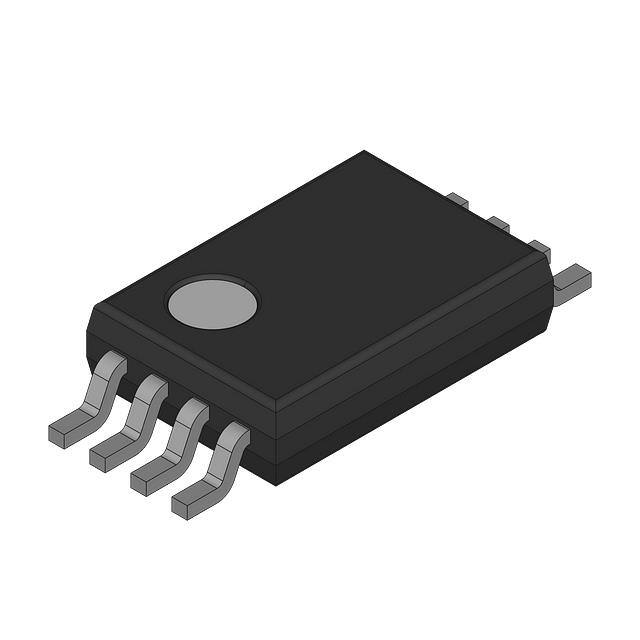
There are 5 products by the difference of packages and the function of voltage detector and watchdog timer.
The packages of R5105N and R5106N are SOT-23-6. The packages of R5107G, R5108G and R5109G are
SSOP-8G.
FEATURES
• Supply Current ...................................................................... Typ. 11µA (R5109G: 11.5µA)
• Operating Voltage Range ..................................................... 0.9V to 6.0V (R5108G: 1.5V to 6.0V)
< Voltage Detector Part >
• Detector Threshold Range.................................................... Stepwise setting with a step of 0.1V in the
range of 1.5V to 5.5V
• Detector Threshold Accuracy................................................ ±1.0%
• Power-on Reset Delay Time accuracy ................................. ±16%∗ (−40°C ≤ Topt ≤ 105°C)
• Power-on reset delay time of the voltage detector ............... Typ. 370ms with an external capacitor : 0.1µF
< Watchdog Timer Part >
• Built-in a watchdog timer's time out period accuracy ........... ±33%∗ (−40°C ≤ Topt ≤ 105°C)
• Timeout period for watchdog timer ....................................... Typ. 310ms with an external capacitor : 0.1µF
• Reset timer for watchdog timer ............................................. Typ. 34ms with an external capacitor : 0.1µF
• Packages .............................................................................. SOT-23-6 (R5105N, R5106N)
SSOP-8G (R5107G, R5108G, R5109G)
∗) Accuracy to center value of (Min.+Max.)/2
APPLICATIONS
• Supervisory circuit for equipment with using microprocessors.
1
�∗ R5105N is the non-promotional product as of March, 2016.
R510xx
BLOCK DIAGRAMS
R5105Nxx1A
R5105Nxx1C
VDD 3
VDD 3
CD 6
CD 6
Vref2
Vref1
CTW 2
WATCHDOG
TIMER
CLOCK
DETECTOR
Vref2
5 GND
WATCHDOG
TIMER
1 SCK
RESETB 4
VDD 3
SW1
SW1
Vref2
SW2
WATCHDOG
TIMER
Vref1
CLOCK
DETECTOR
5 GND
Vref2
CT
6
1 SCK
RESETB 4
2 INH
∗SW1: "L"=ON,
SW2
WATCHDOG
TIMER
R5107Gxx1C
MR
VDD
CD
CD
RESETB
2
1 SCK
SW2: "H"=ON
VDD
WATCHDOG
TIMER
CLOCK
DETECTOR
5 GND
2 INH
MR
Vref2
Vref1
RESETB 4
R5107Gxx1A
CTW
1 SCK
R5106Nxx1C
VDD 3
6
CLOCK
DETECTOR
5 GND
RESETB 4
R5106Nxx1A
CT
Vref1
CTW 2
Vref1
CLOCK
DETECTOR
GND
Vref2
CTW
WATCHDOG
TIMER
Vref1
CLOCK
DETECTOR
GND
SCK
SCK
INH RESETB
INH
�∗ R5105N is the non-promotional product as of March, 2016.
R510xx
R5108Gxx1A
R5108Gxx1C
SENSE
SENSE
VDD
VDD
CD
CD
Vref2
CTW
Vref1
Vref2
GND
WATCHDOG
TIMER
CLOCK
DETECTOR
SCK
INH
RESETB
CTW
Vref1
GND
WATCHDOG
TIMER
CLOCK
DETECTOR
INH
RESETB
R5109Gxx1A
R5109Gxx1C
VDD
VDD
CD
CD
Vref2
Vref1
Vref2
Vref1
GND
CTW
SCK
WATCHDOG
TIMER
GND
CTW
CLOCK
DETECTOR
SCK1
CLOCK
DETECTOR
SCK2
WATCHDOG
TIMER
CLOCK
DETECTOR
SCK1
CLOCK
DETECTOR
SCK2
RESETB
INH
RESETB
INH
3
�∗ R5105N is the non-promotional product as of March, 2016.
R510xx
SELECTION GUIDE
The detector threshold, and the output type for the ICs can be selected at the users’ request. The selection
can be made with designating the part number as shown below;
Product Name
Package
Quantity per Reel
Pb Free
Halogen Free
R5105Nxx1∗-TR-FE
SOT-23-6
3,000 pcs
Yes
Yes
R5106Nxx1∗-TR-FE
SOT-23-6
3,000 pcs
Yes
Yes
R5107Gxx1∗-TR-FE
SSOP-8G
3,000 pcs
Yes
Yes
R5108Gxx1∗-TR-FE
SSOP-8G
3,000 pcs
Yes
Yes
R5109Gxx1∗-TR-FE
SSOP-8G
3,000 pcs
Yes
Yes
xx : The detector threshold can be designated in the range from 1.5V(15) to 5.5V(55) in 0.1V steps.
∗ : Designation of Output Type
(A) Nch Open Drain
(C) CMOS
SERIES SELECTION
R5105N
Package
With INH pin (Inhibit)
R5106N
4
R5108G
SOT-23-6
R5109G
SSOP-8G
No
Yes
2 clock input
With MR pin (Manual Reset)
R5107G
No
No
Yes
Yes
With SENSE pin
No
Remarks
CD pin and
CTW pin are
combined uses.
No
Yes
No
Operating
Supply Current
Voltage Range
11.5µA
1.5V to 6.0V
�∗ R5105N is the non-promotional product as of March, 2016.
R510xx
PIN CONFIGURATIONS
• SOT-23-6
6
5
• SSOP-8G
4
8 7 6 5
3
1 2 3 4
(mark side)
1
2
PIN DESCRIPTIONS
•
•
R5105N (SOT-23-6)
Pin No.
Symbol
Description
1
SCK
Clock Input Pin from Microprocessor
2
CTW
External Capacitor Pin for setting Reset and Watchdog Timer
Timeout Period
3
VDD
Power supply Pin
4
RESETB
5
GND
6
CD
Output Pin for Reset signal of Watchdog timer and Voltage Detector.
(Output "L" at detecting Detector Threshold and Watchdog Timer
Reset.)
Ground Pin
External Capacitor Pin for Setting delay time of Voltage Detector
R5106N (SOT-23-6)
Pin No.
Symbol
Description
1
SCK
Clock Input Pin from Microprocessor
2
INH
Inhibit Pin ("L": Inhibit the watchdog timer)
3
VDD
Power supply Pin
4
RESETB
5
GND
6
CT
Output Pin for Reset signal of Watchdog timer and Voltage Detector.
(Output "L" at detecting Detector Threshold and Watchdog Timer
Reset.)
Ground Pin
External Capacitor Pin for Setting Reset and Watchdog Timeout
Periods and delay time of Voltage Detector
5
�∗ R5105N is the non-promotional product as of March, 2016.
R510xx
•
•
•
6
R5107G (SSOP-8G)
Pin No.
Symbol
Description
1
RESETB
2
MR
Manual Reset Pin (Active"L")
3
CD
External Capacitor Pin for Setting Delay Time of Voltage Detector
4
GND
Ground Pin
5
SCK
Clock Input Pin from Microprocessor
6
INH
Inhibit Pin ("L": Inhibit the watchdog timer)
7
CTW
External Capacitor Pin for Setting Reset and Watchdog Timeout Periods
8
VDD
Power supply Pin
Output Pin for Reset signal of Watchdog timer and Voltage Detector.
(Output "L" at detecting Detector Threshold and Watchdog Timer
Reset.)
R5108G (SSOP-8G)
Pin No.
Symbol
Description
1
RESETB
2
SENSE
3
CD
4
GND
Ground Pin
5
SCK
Clock Input Pin from Microprocessor
6
INH
Inhibit Pin ("L": Inhibit the watchdog timer)
7
CTW
External Capacitor Pin for Setting Reset and Watchdog Timeout Periods
8
VDD
Power supply Pin
Output Pin for Reset signal of Watchdog timer and Voltage Detector.
(Output "L" at detecting Detector Threshold and Watchdog Timer
Reset.)
Voltage Detector Voltage SENSE Pin (Active"L")
External Capacitor Pin for Setting Delay Time of Voltage Detector
R5109G (SSOP-8G)
Pin No.
Symbol
Description
1
RESETB
2
INH
Inhibit Pin ("L": Inhibit the watchdog timer)
3
CD
External Capacitor Pin for Setting Delay Time of Voltage Detector
4
GND
Ground Pin
5
SCK1
Clock Input Pin 1 from Microprocessor
6
SCK2
Clock Input Pin 2 from Microprocessor
7
CTW
External Capacitor Pin for Setting Reset and Watchdog Timeout Periods
8
VDD
Power supply Pin
Output Pin for Reset signal of Watchdog timer and Voltage Detector.
(Output "L" at detecting Detector Threshold and Watchdog Timer
Reset.)
�∗ R5105N is the non-promotional product as of March, 2016.
R510xx
ABSOLUTE MAXIMUM RATINGS
Symbol
Rating
Unit
−0.3 to 7.0
V
Voltage of CD Pin
−0.3 to VDD + 0.3
V
Voltage of CTW Pin
−0.3 to VDD + 0.3
V
Voltage of CT Pin
−0.3 to VDD + 0.3
V
Voltage of RESETB Pin
−0.3 to 7.0
V
Voltage of SCK Pin
−0.3 to 7.0
V
Voltage of INH Pin
−0.3 to 7.0
V
Voltage of MR Pin
−0.3 to 7.0
V
Voltage of SENSE Pin
−0.3 to 7.0
V
Current of RESETB Pin
20
mA
Power Dissipation (SOT-23-6)∗
420
mW
Power Dissipation (SSOP-8G)∗
380
mW
Topt
Operating Temperature Range
−40 to 105
°C
Tstg
Storage Temperature Range
−55 to 125
°C
VDD
Item
Topt=25°C
Supply Voltage
VCD
VCTW
VCT
Output Voltage
VRESETB
VSCK
VINH
VMR
Input Voltage
VSENSE
IRESETB
PD
Output Current
∗ ) For Power Dissipation, please refer to PACKAGE INFORMATION.
ABSOLUTE MAXIMUM RATINGS
Electronic and mechanical stress momentarily exceeded absolute maximum ratings may cause the
permanent damages and may degrade the life time and safety for both device and system using the device
in the field.
The functional operation at or over these absolute maximum ratings is not assured.
7
�∗ R5105N is the non-promotional product as of March, 2016.
R510xx
ELECTRICAL CHARACTERISTICS
VDD=6.0V, CTW=0.1µF, CD=0.1µF, CT=0.1µF, In case of Nch Open Drain Output type, the output pin is pulled up
with a resistance of 100kΩ (R510xxxx1A), unless otherwise noted.
The specification in
is checked and guaranteed by design engineering at −40°C ≤ Topt ≤ 105°C.
•
R5105Nxx1A/C
Symbol
Topt=25°C
Item
VDD
Operating Voltage
ISS
Supply Current
VD Part
Symbol
Detector Threshold
VHYS
Detector Threshold Hysteresis
∆-VDET/ Detector Threshold
∆Topt Temperature Coefficient
IRESETB
Output Delay Time
Output Current
(RESETB Output pin)
WDT Part
Symbol
Item
Min.
Typ.
Max.
Unit
6.0
V
11
15
µA
Typ.
Max.
Unit
0.9
VDD= -VDET+0.5V,
Clock pulse input
Item
-VDET
tPLH
Conditions
Conditions
Min.
Topt=25°C
×0.990
×1.010
−40°C ≤ Topt ≤ 105°C
×0.972
×1.015
-VDET
×0.03
−40°C ≤ Topt ≤ 105°C
CD=0.1µF ∗1
-VDET
×0.05
-VDET
×0.07
370
V
ppm/°C
±100
340
V
467
ms
Nch
VDD=1.2V
VDS=0.1V
0.38
0.8
mA
Pch ∗2
VDD=6.0V
VDS=0.5V
0.65
0.9
mA
Min.
Typ.
Max.
Unit
230
310
450
ms
29
34
48
ms
Conditions
∗1
tWD
Watchdog Timeout period
CTW=0.1µF
tWR
Reset Hold Time of WDT
CTW=0.1µF ∗1
VSCKH
SCK Input "H"
VDD×0.8
6.0
V
VSCKL
SCK Input "L"
0
VDD×0.2
V
tSCKW
SCK Input Pulse Width
VSCKL=VDD×0.2
VSCKH=VDD×0.8
500
ns
All of unit are tested and specified under load conditions such that Topt=25°C except for Detector Threshold
Temperature Coefficient.
∗1) The specification does not contain the temperature characteristics of the external capacitor.
∗2) In case of CMOS type (R5105Nxx1C)
RECOMMENDED OPERATING CONDITIONS (ELECTRICAL CHARACTERISTICS)
All of electronic equipment should be designed that the mounted semiconductor devices operate within the
recommended operating conditions. The semiconductor devices cannot operate normally over the
recommended operating conditions, even if when they are used over such conditions by momentary
electronic noise or surge. And the semiconductor devices may receive serious damage when they continue
to operate over the recommended operating conditions.
8
�∗ R5105N is the non-promotional product as of March, 2016.
R510xx
•
Topt=25°C
R5106Nxx1A/C
Symbol
Item
VDD
Operating Voltage
ISS
Supply Current
VD Part
Symbol
Detector Threshold
VHYS
Detector Threshold Hysteresis
∆-VDET/ Detector Threshold
∆Topt Temperature Coefficient
IRESETB
Min.
Typ.
Max.
Unit
6.0
V
11
15
µA
Typ.
Max.
Unit
0.9
VDD= -VDET+0.5V,
Clock pulse input
Item
-VDET
tPLH
Conditions
Conditions
Min.
Topt=25°C
×0.990
×1.010
−40°C ≤ Topt ≤ 105°C
×0.972
×1.015
-VDET
×0.03
−40°C ≤ Topt ≤ 105°C
-VDET
×0.05
-VDET
×0.07
V
V
ppm/°C
±100
Output Delay Time
CT=0.1µF ∗1
340
370
Output Current
(RESETB Output pin)
Nch
VDD=1.2V, VDS=0.1V
0.38
0.8
mA
Pch ∗2
VDD=6.0V, VDS=0.5V
0.65
0.9
mA
Conditions
Min.
Typ.
Max.
Unit
230
310
450
ms
29
34
48
ms
WDT Part
Symbol
Item
∗1
tWD
Watchdog Timeout period
CT=0.1µF
tWR
Reset Hold Time of WDT
CT=0.1µF ∗1
467
ms
VSCKH
SCK Input "H"
VDD×0.8
6.0
V
VSCKL
SCK Input "L"
0
VDD×0.2
V
VINHH
INH Input "H"
1.0
6.0
V
VINHL
INH Input "L"
0
0.35
V
RINH
INH pull-up Resistance
60
164
kΩ
tSCKW
SCK Input Pulse Width
VSCKL=VDD×0.2
VSCKH=VDD×0.8
110
500
ns
All of unit are tested and specified under load conditions such that Topt=25°C except for Detector Threshold
Temperature Coefficient.
∗1) The specification does not contain the temperature characteristics of the external capacitor.
∗2) In case of CMOS type (R5106Nxx1C)
RECOMMENDED OPERATING CONDITIONS (ELECTRICAL CHARACTERISTICS)
All of electronic equipment should be designed that the mounted semiconductor devices operate within the
recommended operating conditions. The semiconductor devices cannot operate normally over the
recommended operating conditions, even if when they are used over such conditions by momentary
electronic noise or surge. And the semiconductor devices may receive serious damage when they continue
to operate over the recommended operating conditions.
9
�∗ R5105N is the non-promotional product as of March, 2016.
R510xx
•
Topt=25°C
R5107Gxx1A/C
Symbol
Item
VDD
Operating Voltage
ISS
Supply Current
VD Part
Symbol
Conditions
VDD= -VDET+0.5V,
Clock pulse input
Item
Conditions
Detector Threshold
VHYS
Detector Threshold Hysteresis
∆-VDET/ Detector Threshold
∆Topt Temperature Coefficient
IRESETB
6.0
V
11
15
µA
Min.
Typ.
Max.
Unit
Topt=25°C
×0.990
×1.010
−40°C ≤ Topt ≤ 105°C
×0.972
×1.015
-VDET
×0.03
−40°C ≤ Topt ≤ 105°C
-VDET
×0.05
-VDET
×0.07
V
V
ppm/°C
±100
340
370
Output Current
(RESETB Output pin)
Nch
VDD=1.2V, VDS=0.1V
0.38
0.8
mA
VDD=6.0V, VDS=0.5V
0.65
0.9
mA
VMRL
MR Input "L"
Pch
∗2
∗3
MR Input Pulse Width
∗4
RMR
MR Pull-up Resistance
WDT Part
Symbol
Item
tWR
Unit
CD=0.1µF ∗1
MR Input "H"
tWD
Max.
Output Delay Time
VMRH
tMRW
Typ.
0.9
-VDET
tPLH
Min.
Watchdog Timeout period
Reset Hold Time of WDT
467
1.0
6.0
V
0
0.35
V
3
Conditions
CTW=0.1µF ∗1
CTW=0.1µF
∗1
ms
µs
60
110
164
kΩ
Min.
Typ.
Max.
Unit
230
310
450
ms
29
34
48
ms
VSCKH
SCK Input "H"
VDD×0.8
6.0
V
VSCKL
SCK Input "L"
0
VDD×0.2
V
VINHH
INH Input "H"
1.0
6.0
V
VINHL
INH Input "L"
0
0.35
V
RINH
INH pull-up Resistance
64
152
kΩ
tSCKW
SCK Input Pulse Width
VSCKL=VDD×0.2
VSCKH=VDD×0.8
110
500
ns
All of unit are tested and specified under load conditions such that Topt=25°C except for Detector Threshold
Temperature Coefficient and MR Input Pulse Width.
∗1) The specification does not contain the temperature characteristics of the external capacitor.
∗2) In case of CMOS type (R5107Gxx1C)
∗3) In case of Nch open drain type (R5107Gxx1A)
∗4) MR input pulse width specification guarantee the minimum input pulse width of MR pin for output "L" from RESETB pin.
If the "L" pulse width of MR is short, tPLH may be short. Refer to the timing diagram for details.
RECOMMENDED OPERATING CONDITIONS (ELECTRICAL CHARACTERISTICS)
All of electronic equipment should be designed that the mounted semiconductor devices operate within the
recommended operating conditions. The semiconductor devices cannot operate normally over the
recommended operating conditions, even if when they are used over such conditions by momentary
electronic noise or surge. And the semiconductor devices may receive serious damage when they continue
to operate over the recommended operating conditions.
10
�∗ R5105N is the non-promotional product as of March, 2016.
R510xx
•
Topt=25°C
R5108Gxx1A/C
Symbol
Item
VDD
Operating Voltage
ISS
Supply Current
VD Part
Symbol
Detector Threshold
VHYS
Detector Threshold
Hysteresis
∆-VDET/ Detector Threshold
∆Topt Temperature Coefficient
IRESETB
VDDL
Output Delay Time
Output Current
(RESETB Output pin)
Min.
VDD= -VDET+0.5V,
Clock pulse input
Conditions
VDD=5V,
Topt=25°C
SENSE pin
Threshold −40°C≤Topt≤105°C
Min.
Item
Max.
Unit
6.0
V
11
15
µA
Typ.
Max.
Unit
×0.990
×1.010
×0.972
×1.015
-VDET
×0.03
−40°C ≤ Topt ≤ 105°C
CD=0.1µF ∗1
-VDET
×0.05
-VDET
×0.07
340
370
V
V
ppm/°C
±100
467
ms
Nch
VDD=1.2V
VDS=0.1V
0.38
0.8
mA
Pch ∗2
VDD=6.0V
VDS=0.5V
0.65
0.9
mA
Minimum Operating Voltage RESETB ≤ 0.1V, pull-up=100kΩ
WDT Part
Symbol
Typ.
1.5
Item
-VDET
tPLH
Conditions
Conditions
∗1
tWD
Watchdog Timeout period
CTW=0.1µF
tWR
Reset Hold Time of WDT
CTW=0.1µF ∗1
0.6
0.9
V
Min.
Typ.
Max.
Unit
230
310
450
ms
29
34
48
ms
VSCKH
SCK Input "H"
VDD×0.8
6.0
V
VSCKL
SCK Input "L"
0
VDD×0.2
V
VINHH
INH Input "H"
1.0
6.0
V
VINHL
INH Input "L"
0
0.35
V
RINH
INH pull-up Resistance
60
164
kΩ
tSCKW
SCK Input Pulse Width
VSCKL=VDD×0.2
VSCKH=VDD×0.8
110
500
ns
All of unit are tested and specified under load conditions such that Topt=25°C except for Detector Threshold
Temperature Coefficient.
∗1) The specification does not contain the temperature characteristics of the external capacitor.
∗2) In case of CMOS type (R5108Gxx1C)
RECOMMENDED OPERATING CONDITIONS (ELECTRICAL CHARACTERISTICS)
All of electronic equipment should be designed that the mounted semiconductor devices operate within the
recommended operating conditions. The semiconductor devices cannot operate normally over the
recommended operating conditions, even if when they are used over such conditions by momentary
electronic noise or surge. And the semiconductor devices may receive serious damage when they continue
to operate over the recommended operating conditions.
11
�∗ R5105N is the non-promotional product as of March, 2016.
R510xx
•
Topt=25°C
R5109Gxx1A/C
Symbol
Item
VDD
Operating Voltage
ISS
Supply Current
VD Part
Symbol
Detector Threshold
VHYS
Detector Threshold Hysteresis
∆-VDET/ Detector Threshold
∆Topt Temperature Coefficient
IRESETB
Output Delay Time
Output Current
(RESETB Output pin)
WDT Part
Symbol
Item
Min.
Typ.
Max.
Unit
6.0
V
11.5
15.5
µA
Typ.
Max.
Unit
0.9
VDD= -VDET+0.5V,
Clock pulse input
Item
-VDET
tPLH
Conditions
Conditions
Min.
Topt=25°C
×0.990
×1.010
−40°C ≤ Topt ≤ 105°C
×0.972
×1.015
-VDET
×0.03
−40°C ≤ Topt ≤ 105°C
CD=0.1µF ∗1
-VDET
×0.05
-VDET
×0.07
370
V
ppm/°C
±100
340
V
467
ms
Nch
VDD=1.2V
VDS=0.1V
0.38
0.8
mA
Pch ∗2
VDD=6.0V
VDS=0.5V
0.65
0.9
mA
Min.
Typ.
Max.
Unit
Conditions
tWD
Watchdog Timeout period
CTW=0.1µF ∗1
230
310
450
ms
tWR
Reset Hold Time of WDT
CTW=0.1µF ∗1
29
34
48
ms
VSCKH
SCK Input "H"
SCK1, SCK2
VDD×0.8
6.0
V
VSCKL
SCK Input "L"
SCK1, SCK2
0
VDD×0.2
V
VINHH
INH Input "H"
1.0
6.0
V
VINHL
INH Input "L"
0
0.35
V
RINH
INH pull-up Resistance
60
164
kΩ
tSCKW
SCK Input Pulse Width
VSCKL=VDD×0.2
VSCKH=VDD×0.8
110
500
ns
All of unit are tested and specified under load conditions such that Topt=25°C except for Detector Threshold
Temperature Coefficient.
∗1) The specification does not contain the temperature characteristics of the external capacitor.
∗2) In case of CMOS type (R5109Gxx1C)
RECOMMENDED OPERATING CONDITIONS (ELECTRICAL CHARACTERISTICS)
All of electronic equipment should be designed that the mounted semiconductor devices operate within the
recommended operating conditions. The semiconductor devices cannot operate normally over the
recommended operating conditions, even if when they are used over such conditions by momentary
electronic noise or surge. And the semiconductor devices may receive serious damage when they continue
to operate over the recommended operating conditions.
12
�∗ R5105N is the non-promotional product as of March, 2016.
R510xx
TIMING CHART
• R5105N
VDD
+VDET
-VDET
tPHL
VCD
tPHL
+VTCD
-VTCD
tWD
Vref2H
tWDI
VCTW
Vref2L
tPLH
tPLH
VSCK
tWR
VRESETB
(1)
(2)
(3)
(4) (1)
∗) VTCD : Threshold voltage of CD pin when a power-on reset pulse inverting.
∗) Vref2H : CTW pin voltage at the end of WDT timeout period.
∗) Vref2L : CTW pin voltage at the begin of WDT timeout period.
OPERATION
(1) When the power supply, VDD pin voltage becomes more than the released voltage (+VDET), after the released
delay time (or the power on reset time tPLH), the output of RESETB becomes "H" level.
(2) When the SCK pulse is input, the watchdog timer (WDT) is cleared, and CTW pin mode changes from the
discharge mode to the charge mode. When the CTW pin voltage becomes higher than VrefH, the mode will
change into the discharge mode, and next watchdog time count starts.
13
�∗ R5105N is the non-promotional product as of March, 2016.
R510xx
(3) Unless the SCK pulse is input, WDT will not be cleared, and during the charging period of CTW pin,
RESETB="L".
(4) When the VDD pin becomes lower than the detector threshold voltage(-VDET), RESETB outputs "L".
•
Watchdog Timeout period/Reset hold time
The watchdog timeout period and reset hold time can be set with an external capacitor to CTW pin.
The next equations describe the relation between the watchdog timeout period and the external capacitor
value, or the reset hold time and the external capacitor value.
tWD (s) = 3.1×10⁶×C (F)
tWR (s) = tWD/9
The watchdog timer (WDT) timeout period is determined with the discharge time of the external capacitor.
During the watchdog timeout period, if the clock pulse from the system is detected, WDT is cleared and the
capacitor is charged. When the charge of the capacitor completes, another watchdog timeout period starts again.
During the watchdog timeout period, if the clock pulse from the system is not detected, during the next reset hold
time RESETB pin outputs "L".
During the reset time, (while charging the external capacitor) and after starting the watchdog timeout period,
(just after from the discharge of the external capacitor) even if the clock pulse is input during the time period
"tWDI", the clock pulse is ignored.
tWDI (s) = tWD/10
•
Released Delay Time (Power-on Reset delay time)
The released delay time can be set with an external capacitor connected to the CD pin. The next equation
describes the relation between the capacitance value and the released delay time (tPLH).
tPLH (s) =3.7×10⁶× C (F)
When the VDD voltage becomes equal or less than (-VDET), discharge of the capacitor connected to the CD pin
starts. Therefore, if the discharge is not enough and VDD voltage returns to (+VDET) or more, thereafter the delay
time will be shorter than tPLH which is expected.
Power on Reset Operation against the input glitch (tPLH1