Rx5RE SERIES
VOLTAGE REGULATOR
NO. EA-016-130402
OUTLINE
The Rx5RE Series are CMOS-based voltage regulator ICs with high output voltage accuracy and ultra-low
quiescent current. Each of these ICs consists of a voltage reference unit, an error amplifier, a driver transistor,
and resistors for setting output voltage, and a current limit circuit. By use of these ICs, a constant voltage power
supply circuit with high efficiency can be constructed because the dropout voltage and quiescent current of these
ICs are very small. Furthermore, theses ICs have a built-in current limit circuit. The output voltage of these ICs is
fixed with high accuracy.
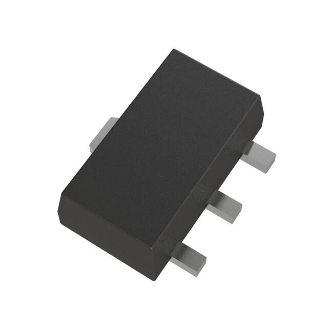
Two types of packages, TO-92 (Discontinued) and SOT-89 (Mini-power Mold) are available.
FEATURES
•
•
•
•
•
•
•
•
•
Supply Current ............................................................. Typ. 1.1μA (VOUT=3.0V, VIN=5.0V)
Dropout Voltage ........................................................... Typ. 0.5V (IOUT=60mA, VOUT=2.8V)
Output Current ............................................................. Typ. 120mA (VOUT=5.0V)
Input Voltage Range .................................................... Max. 10.0V
Output Voltage Range.................................................. 2.0V to 6.0V (0.1V steps)
(For other voltages, please refer to MARK INFORMATIONS.)
Output Voltage Accuracy..............................................±2.5%
Temperature-Drift Coefficient of Output Voltage .......... Typ. ± 100ppm/°C
Line Regulation ............................................................ Typ. 0.1%/V
Packages ..................................................................... SOT-89 (Mini-power Mold),TO-92 (Discontinued)
APPLICATIONS
• Power source for battery-powered equipment
• Power source for cameras, video instruments such as camcorders, VCRs, and hand- held communication
equipment
• Precision voltage references
1
�Rx5RE
BLOCK DIAGRAMS
Rx5RE
VIN
VOUT
2
3
+
–
Vref
1
GND
SELECTION GUIDE
The output voltage and package for the ICs can be selected at the user’s request.
Product Name
RH5RExxAA-T1-FE
RE5RExxAA-TZ-F
Package
Quantity per Reel
Pb Free
Halogen Free
SOT-89
1,000 pcs
Yes
Yes
TO-92 (Discontinued)
2,500 pcs
Yes
No
xx : The output voltage can be designated in the range from 2.0V (20) to 6.0V (60) in 0.1V steps.
(For other voltages, please refer to MARK INFORMATIONS.)
2
�Rx5RE
PIN CONFIGURATION
z SOT-89
z TO-92
(mark side)
(mark side)
1
2
3
1
2
3
PIN DESCRIPTION
•
•
SOT-89
Pin No
Symbol
1
GND
2
VIN
3
VOUT
Pin Description
Ground Pin
Input Pin
Output Pin
TO-92 (Discontinued)
Pin No
Symbol
1
GND
2
VIN
3
VOUT
Pin Description
Ground Pin
Input Pin
Output Pin
3
�Rx5RE
ABSOLUTE MAXIMUM RATINGS
Symbol
VIN
Item
Input Voltage
Rating
Unit
12
V
VOUT
Output Voltage
−0.3 to VIN+0.3
V
IOUT
Output Current
300
mA
∗
Power Dissipation
PD
∗
Power Dissipation
(SOT-89)
900
(TO-92) (Discontinued)
300
mW
Topt
Operating Temperature Range
−40 to 85
°C
Tstg
Storage Temperature Range
−55 to 125
°C
Tsolder
Lead Temperature (Soldering)
260°C,10s
∗) For Power Dissipation, please refer to PACKAGE INFORMATION.
ABSOLUTE MAXIMUM RATINGS
Electronic and mechanical stress momentarily exceeded absolute maximum ratings may cause the
permanent damages and may degrade the life time and safety for both device and system using the device
in the field.
The functional operation at or over these absolute maximum ratings is not assured.
RECOMMENDED OPERATING CONDITIONS (ELECTRICAL CHARACTERISTICS)
All of electronic equipment should be designed that the mounted semiconductor devices operate within the
recommended operating conditions. The semiconductor devices cannot operate normally over the
recommended operating conditions, even if when they are used over such conditions by momentary
electronic noise or surge. And the semiconductor devices may receive serious damage when they continue
to operate over the recommended operating conditions.
4
�Rx5RE
ELECTRICAL CHARACTERISTICS
• Rx5RE20A
Symbol
Topt=25˚C
Item
Conditions
Min.
Typ.
Max.
Unit
2.050
V
VOUT
Output Voltage
VIN=4.0V,IOUT=10mA
1.950
2.000
IOUT
Output Current
VIN=4.0V
40
60
∆VOUT
∆IOUT
VDIF
ISS
∆VOUT
∆VIN
Load Regulation
Dropout Voltage
Quiescent Current
Line Regulation
VIN
Input Voltage
Ilim
Current Limit
∆VOUT
∆Topt
Output Voltage
Temperature Coefficient
VIN=4.0V
mA
40
80
mV
IOUT=30mA
0.5
0.7
V
VIN=4.0V
1.0
3.0
µA
1mA≤IOUT≤50mA
IOUT=10mA
0.1
VOUT+1.0V≤VIN≤10V
%/V
10
IOUT=10mA
–40˚C≤Topt≤85˚C
240
mA
±100
ppm/˚C
• Rx5RE30A
Symbol
Topt=25˚C
Item
Conditions
Min.
Typ.
Max.
Unit
3.075
V
VOUT
Output Voltage
VIN=5.0V,IOUT=10mA
2.925
3.000
IOUT
Output Current
VIN=5.0V
50
80
∆VOUT
∆IOUT
VDIF
ISS
∆VOUT
∆VIN
Load Regulation
Dropout Voltage
Quiescent Current
Line Regulation
VIN
Input Voltage
Ilim
Current Limit
∆VOUT
∆Topt
V
Output Voltage
Temperature Coefficient
VIN=5.0V
mA
40
80
mV
IOUT=40mA
0.5
0.7
V
VIN=5.0V
1.1
3.3
µA
1mA≤IOUT≤60mA
IOUT=10mA
VOUT+1.0V≤VIN≤10V
0.1
%/V
10
IOUT=10mA
–40˚C≤Topt≤85˚C
V
240
mA
±100
ppm/˚C
5
�Rx5RE
• Rx5RE40A
Symbol
Topt=25˚C
Item
Conditions
Min.
Typ.
Max.
Unit
4.100
V
VOUT
Output Voltage
VIN=6.0V,IOUT=10mA
3.900
4.000
IOUT
Output Current
VIN=6.0V
65
100
∆VOUT
∆IOUT
VDIF
ISS
∆VOUT
∆VIN
Load Regulation
Dropout Voltage
Quiescent Current
Line Regulation
VIN
Input Voltage
Ilim
Current Limit
∆VOUT
∆Topt
Output Voltage
Temperature Coefficient
VIN=6.0V
mA
40
80
mV
IOUT=50mA
0.5
0.7
V
VIN=6.0V
1.2
3.6
µA
1mA≤IOUT≤70mA
IOUT=10mA
0.1
VOUT+1.0V≤VIN≤10V
%/V
10
IOUT=10mA
–40˚C≤Topt≤85˚C
240
mA
±100
ppm/˚C
• Rx5RE50A
Symbol
Item
Conditions
Min.
Typ.
Max.
Unit
5.125
V
Output Voltage
VIN=7.0V,IOUT=10mA
4.875
5.000
IOUT
Output Current
VIN=7.0V
80
120
∆IOUT
VDIF
ISS
∆VOUT
∆VIN
Load Regulation
Dropout Voltage
Quiescent Current
Line Regulation
VIN
Input Voltage
Ilim
Current Limit
∆VOUT
∆Topt
6
Topt=25˚C
VOUT
∆VOUT
V
Output Voltage
Temperature Coefficient
VIN=7.0V
mA
40
80
mV
IOUT=60mA
0.5
0.7
V
VIN=7.0V
1.3
3.9
µA
1mA≤IOUT≤80mA
IOUT=10mA
VOUT+1.0V≤VIN≤10V
0.1
%/V
10
IOUT=10mA
–40˚C≤Topt≤85˚C
V
240
mA
±100
ppm/˚C
�Rx5RE
• Rx5RE60A
Symbol
Topt=25˚C
Item
Conditions
Min.
Typ.
Max.
Unit
6.150
V
VOUT
Output Voltage
VIN=8.0V,IOUT=10mA
5.850
6.000
IOUT
Output Current
VIN=8.0V
80
120
∆VOUT
∆IOUT
VDIF
ISS
∆VOUT
∆VIN
Load Regulation
Dropout Voltage
Quiescent Current
Line Regulation
VIN
Input Voltage
Ilim
Current Limit
∆VOUT
∆Topt
Output Voltage
Temperature Coefficient
VIN=8.0V
mA
40
80
mV
IOUT=60mA
0.5
0.7
V
VIN=8.0V
1.4
4.2
µA
1mA≤IOUT≤80mA
IOUT=10mA
VOUT+1.0V≤VIN≤10V
0.1
%/V
10
IOUT=10mA
–40˚C≤Topt≤85˚C
V
240
mA
±100
ppm/˚C
7
�Rx5RE
ELECTRICAL CHARACTERISTICS BY OUTPUT VOLTAGE
Output Voltage
VOUT(V)
Part Number
Conditions
Rx5RE20A
Rx5RE21A
Rx5RE22A
Rx5RE23A
Rx5RE24A
Rx5RE25A
Rx5RE26A
Rx5RE27A
Rx5RE28A
Rx5RE29A
Rx5RE30A
Rx5RE31A
Rx5RE32A
Rx5RE33A
Rx5RE34A
Rx5RE35A
Rx5RE36A
Rx5RE37A
Rx5RE38A
Rx5RE39A
Rx5RE40A
Rx5RE41A
Rx5RE42A
Rx5RE43A
Rx5RE44A
Rx5RE45A
Rx5RE46A
Rx5RE47A
Rx5RE48A
Rx5RE49A
Rx5RE50A
Rx5RE51A
Rx5RE52A
Rx5RE53A
Rx5RE54A
Rx5RE55A
Rx5RE56A
Rx5RE57A
Rx5RE58A
Rx5RE59A
Rx5RE60A
8
OutputCurrent
Min.
1.950
2.048
2.145
2.243
2.340
2.438
2.535
2.633
2.730
2.828
2.925
3.023
3.120
3.218
3.315
3.413
VIN– 3.510
VOUT 3.608
=2.0V 3.705
3.803
3.900
3.998
IOUT
4.095
=10mA 4.193
4.290
4.388
4.485
4.583
4.680
4.778
4.875
4.973
5.070
5.168
5.265
5.363
5.460
5.558
5.655
5.753
5.850
IOUT(mA)
Typ.
Max.
2.000
2.100
2.200
2.300
2.400
2.500
2.600
2.700
2.800
2.900
3.000
3.100
3.200
3.300
3.400
3.500
3.600
3.700
3.800
3.900
4.000
4.100
4.200
4.300
4.400
4.500
4.600
4.700
4.800
4.900
5.000
5.100
5.200
5.300
5.400
5.500
5.600
5.700
5.800
5.900
6.000
2.050
2.152
2.255
2.357
2.460
2.562
2.665
2.767
2.870
2.972
3.075
3.177
3.280
3.382
3.485
3.587
3.690
3.792
3.895
3.997
4.100
4.202
4.305
4.407
4.510
4.612
4.715
4.817
4.920
5.022
5.125
5.227
5.330
5.432
5.535
5.637
5.740
5.842
5.945
6.047
6.150
Conditions
Min.
Typ.
Load Regulation
Dropout Voltage
∆VOUT/∆IOUT(mV)
VDIF(V)
Conditions
Typ.
Max.
Conditions
Typ.
Max.
0.5
0.7
VIN–
VOUT
=2.0V
40
60
1mA≤
IOUT
≤50mA
IOUT
=30mA
VIN–
VOUT
=2.0V
1mA≤
IOUT
≤60mA
50
IOUT
80
=40mA
VIN–
VIN–
VOUT
VOUT
=2.0V
=2.0V
40
80
1mA≤
IOUT
≤70mA
65
IOUT
100
=50mA
VIN–
VOUT
=2.0V
80
120
1mA≤
IOUT
IOUT
=60mA
≤80mA
�Rx5RE
Topt=25˚C
Quiescent Current
∆VOUT/∆VI N(%/V) VI N(V) Ilim(mA) ∆VOUT/∆T(ppm/˚C)
Iss(µA)
Conditions
Line Regulation Input Voltage Current Limit Output Voltage Tempco.
Typ.
Max.
1.0
3.0
1.1
3.3
Conditions
Typ.
Max.
Typ.
Conditions
Typ.
IOUT
=10mA
VIN–
VOUT
IOUT
=10mA
1.2
3.6
=2.0V
0.1
VOUT+
10
240
±100
–40˚C≤
1.0V≤
Topt
VIN
≤85˚C
≤10V
1.3
3.9
1.4
4.2
9
�Rx5RE
OPERATION
Output voltage VOUT divided at the node between registers R1 and R2 is compared with reference voltage by
VOUT
VIN
error amplifier, so that a constant voltage is output.
Error Amplifire
–
R1
+
Vref
R2
GND
GND
FIG. 1 Brock Diagram
TEST CIRCUITS
VIN
VIN
CI
1µF
+
VOUT
Rx5RE
SERIES
IOUT
ISS
VOUT
+ Co
1µF
GND
P.G
Rx5RE
SERIES
VOUT
+
Ro
Co
0.1µF
FIG. 4 Line Transient Response Test Circuit
10
Rx5RE
SERIES
VOUT
GND
FIG. 3 Quiescent Current Test Circuit
VOUT
GND
VIN
CI +
1µF
FIG. 2 Test Circuit
VIN
VIN
�Rx5RE
TYPICAL CHARACTERISTICS
1) Output Voltage vs. Output Current
Rx5RE30A
3.1
Rx5RE40A
VIN=5.0V
VIN=6.0V
4.1
Output Voltage VOUT(V)
Output Voltage VOUT(V)
Topt= –40˚C
3.0
25˚C
2.9
85˚C
2.8
Topt=–40˚C
4.0
25˚C
3.9
3.8
85˚C
2.7
3.7
0
50
100
150
200
Output Current IOUT(mA)
Rx5RE50A
5.1
250
0
150
50
100
Output Current IOUT(mA)
Rx5RE50A
VIN=7.0V
200
VIN=7.0V
5.1
5.0
25˚C
4.9
85˚C
4.8
Output Voltage VOUT(V)
Output Voltage VOUT(V)
Topt=–40˚C
5.0
with heatsink
4.9
without heatsink
4.8
heatsink
30×30×1mm
4.7
4.7
0
50 100 150 200 250 300 350
Output Current IOUT(mA)
0
50
100
150
200
Output Current IOUT(mA)
250
2) Output Voltage vs. Input Voltage
Rx5RE20A
2.4
IOUT=1µA
2.0
1.8
1.6
10mA
1.4
1.2
1.0
0.8
1.0
1mA
Topt=25˚C
2.04
Output Voltage VOUT(V)
Output Voltage VOUT(V)
2.2
Rx5RE20A
Topt=25˚C
2.02
IOUT=1µA
2.00
1mA
10mA
1.98
1.96
2.0
3.0
4.0
Input Voltage VIN(V)
5.0
2
3
4
5
6
Input Voltage VIN(V)
7
11
�Rx5RE
Rx5RE30A
3.4
Rx5RE30A
Topt=25˚C
Topt=25˚C
3.00
IOUT=1mA
2.8
2.6
50mA
2.4
2.2
10mA
2.0
1.8
2.0
2.5
3.0
3.5
4.0
Input Voltage VIN(V)
Rx5RE40A
4.2
Output Voltage VOUT(V)
Output Voltage VOUT(V)
3.0
2.99
IOUT=1µA
2.98
1mA
2.97
10mA
2.96
2.95
3.0
4.5
4.0
5.0
6.0
7.0
Input Voltage VIN(V)
Rx5RE40A
Topt=25˚C
8.0
Topt=25˚C
4.06
4.0
Output Voltage VOUT(V)
Output Voltage VOUT(V)
3.2
IOUT=1mA
3.8
3.6
50mA
3.4
4.04
4.02
IOUT=1µA
4.00
1mA
10mA
3.98
10mA
3.96
3.5
4.5
5.5
Input Voltage VIN(V)
Rx5RE50A
Output Voltage VOUT(V)
5.1
5.0
4.8
4.6
IOUT=1mA
10mA
50mA
5
6
7
8
Input Voltage VIN(V)
9
Rx5RE50A
Topt=25˚C
4.4
4.2
4.0
12
4
Topt=25˚C
5.05
5.04
Output Voltage VOUT(V)
3.2
2.5
5.03
5.02
5.01
IOUT=1µA
5.00
4.99
4.98
1mA 10mA
4.97
4.96
4.95
4.5
5.0
5.5
6.0
Input Voltage VIN(V)
6.5
5
6
7
8
9
Input Voltage VIN(V)
10
�Rx5RE
3) Dropout Voltage vs. Output Curret
Rx5RE30A
Rx5RE40A
1.0
1.2
Dropout Voltage VDIF(V)
Dropout Voltage VDIF(V)
1.4
85˚C
1.0
0.8
25˚C
0.6
0.4
0.2
0.8
85˚C
0.6
25˚C
0.4
0.2
Topt=–40˚C
Topt=–40˚C
0.0
0.0
0
20
40
60
80
Output Current IOUT(mA)
0
100
20
40
60
80
Output Current IOUT(mA)
100
Rx5RE50A
0.8
Dropout Voltage VDIF(V)
0.7
0.6
85˚C
0.5
25˚C
0.4
0.3
0.2
Topt= –40˚C
0.1
0.0
0
20
40
60
80
Output Current IOUT(mA)
100
4) Output Voltage vs.Temperature
Rx5RE30A
3.0
2.9
-50 -30 -10 10 30 50 70
Temperature Topt(˚C)
4.1
Output Voltage VOUT(V)
Output Voltage VOUT(V)
3.1
Rx5RE40A
IOUT=10mA
90
IOUT=10mA
4.0
3.9
-50 -30 -10 10 30 50 70
Temperature Topt(˚C)
90
13
�Rx5RE
Rx5RE50A
Output Voltage VOUT(V)
5.2
IOUT=10mA
5.1
5.0
4.9
4.8
-50 -30 -10 10 30 50 70
Temperature Topt(˚C)
90
5) Quiescent Current vs. Input Voltage
Rx5RE20A
Rx5RE30A
Topt=25˚C
1.4
Quiescent Current Iss(µA)
Quiescent Current Iss(µA)
1.1
1.0
0.9
0.8
0.7
Topt=25˚C
1.3
1.2
1.1
1.0
0.6
3
4
5
6
7
8
Input Voltage VIN(V)
9
10
2
3
4
5 6
7 8
Input Voltage VIN(V)
10
Rx5RE50A
Rx5RE40A
Topt=25˚C
1.5
9
Topt=25˚C
1.5
Quiescent Current Iss(µA)
Quiescent Current Iss(µA)
1.4
1.4
1.3
1.2
1.1
1.3
1.2
1.1
1.0
0.9
0.8
0.7
0.6
1.0
14
4
5
6
7
8
9 10
Input Voltage VIN(V)
11
0.5
5
6
7
8
9 10 11
Input Voltage VIN(V)
12
�Rx5RE
Rx5RE30A
1.5
1.5
1.4
1.4
Quiescent Current Iss(µA)
Quiescent Current Iss(µA)
6) Quiescent Current vs. Temperature
Rx5RE20A
1.3
1.2
1.1
1.0
0.9
0.8
0.7
0.6
1.3
1.2
1.1
1.0
0.9
0.8
0.7
0.6
0.5
–50 –30 –10 10 30 50 70
Temperature Topt(˚C)
0.5
–50 –30 –10 10 30 50 70
Temperature Topt(˚C)
90
90
Rx5RE40A
1.5
Quiescent Current Iss(µA)
1.4
1.3
1.2
1.1
1.0
0.9
0.8
0.7
0.6
0.5
–50 –30 –10 10 30 50 70
Temperature Topt(˚C)
90
7) Dropout Voltage vs. Set Output Voltage
Rx5RE SERIES Topt=25˚C
Dropout Voltage VDIF(V)
0.7
0.6
0.5
IOUT=50mA
0.4
0.3
0.2
10mA
0.1
1mA
0.0
0
1
2
3
4
5
Set Output Voltage Vreg(V)
6
15
�Rx5RE
4.5
Input Voltage
3.5
3.0
2.5
Output Voltage
2.0
1.5
2.0
2.5 3.0 3.5
Time t(ms)
Rx5RE40A
8.0
Input Voltage/Output Voltage V(V)
Input Voltage/Output Voltage V(V)
4.5
1.0
1.5
4.0
6.0
5.0
Output Voltage
4.0
3.0
2.0
2.5 3.0 3.5
Time t(ms)
4.0
6.0
5.0
Input Voltage
4.0
Output Voltage
3.0
2.0
2.0
2.5 3.0 3.5
Time t(ms)
Rx5RE50A
IOUT=1mA
Input Voltage
IOUT=1mA
7.0
1.0
1.5
4.5
7.0
2.0
1.5
Rx5RE30A
IOUT=1mA
5.0
4.5
8.0
7.0
Input Voltage
6.0
Output Voltage
5.0
4.0
3.0
0
4.5
4.0
IOUT=1mA
9.0
Input Voltage/Output Voltage V(V)
Input Voltage/Output Voltage V(V)
8) Line Transient Response (1)
Rx5RE20A
0.5 1.0 1.5 2.0 2.5 3.0 3.5 4.0
Time t(ms)
9) Line Transient Response (2)
4.5
4.0
3.5
3.0
Output Voltage
2.0
1.5
1.0
0.5
0.0
1.5
16
Input Voltage
2.5
2.0
Rx5RE30A
IOUT=30mA
Input Voltage/Output Voltage V(V)
Input Voltage/Output Voltage V(V)
Rx5RE20A
5.0
2.5 3.0 3.5
Time t(ms)
4.0
4.5
7.0
IOUT=30mA
6.0
5.0
Input Voltage
4.0
Output Voltage
3.0
2.0
1.0
1.5
2.0
2.5 3.0 3.5
Time t(ms)
4.0
4.5
�Rx5RE
8.0
7.0
Input Voltage
6.0
5.0
Output Voltage
4.0
3.0
2.0
1.5
2.0
Rx5RE50A
IOUT=30mA
2.5 3.0 3.5
Time t(ms)
9.0
Input Voltage/Output Voltage V(V)
Input Voltage/Output Voltage V(V)
Rx5RE40A
4.0
4.5
IOUT=30mA
8.0
7.0
Input Voltage
6.0
Output Voltage
5.0
4.0
3.0
0
0.5 1.0 1.5 2.0 2.5 3.0 3.5 4.0
Time t(ms)
17
�Rx5RE
TYPICAL APPLICATION
In Rx5RE Series, a constant voltage can be obtained
VIN
VIN
C1
+
VOUT
Rx5RE
SERIES
+
VOUT
without using capacitors C1 and C2. However, when the
wire connected to VIN is long, use capacitor C1. Output
C2
GND
noise can be reduced by using capacitor C2.
Insert capacitors C1 and C2 with the capacitance of
GND
GND
0.1µF to 2.0µF between input/output pins and GND pin
with minimum wiring.
APPLICATION CIRCUITS
• VOLTAGE BOOST CIRCUIT
The output voltage can be obtained by the following formula :
VIN
VIN
Rx5RE
SERIES
VOUT
GND
C1
VOUT
+
Since the quiescent current of Rx5RE Series is so
C2
R1
small that the resistances of R1 and R2 can be set as
ISS
+
1
VOUT=Vreg* · (1+R2/R1) + ISS · R2
large as several hundreds kΩ and therefore the sup-
GND
ply current of “Voltage Boost Circuit” itself can be
R2
reduced.
Furthermore, since Rx5RE Series are operated by
a constant voltage, the supply current of “Voltage
Boost Circuit” is not substantially affected by the
input voltage.
*1) Vreg : Set Output Voltage of Rx5RE Series.
• DUAL POWER SUPPLY CIRCUIT
As shown in the circuit diagram, a dual power supply circuit can be constructed by using two Rx5RE
IC1
VIN
VIN
Rx5RE20A
VOUT
C1
VOUT1
5V
+
D
When the minimum output current of IC2 is larger
IC2
VOUT
VIN
VOUT2
3V
Rx5RE30A
C2
+
C3
+
R
GND
GND
18
This circuit diagram shows a dual power supply
circuit with an output of 3V and an output of 5V.
ISS
GND
Series.
GND
than ISS of IC1, resistor R is unnecessary. Diode D is
a protection diode for the case where VOUT2
becomes larger than VOUT1.
�Rx5RE
• CURRENT BOOST CIRCUIT
Output current of 120mA or more can be obtained
Tr.1
by the current boost circuit constructed as shown in
this circuit diagram.
VIN
VIN
VOUT
Rx5RE
SERIES
VOUT
+
C1
+
C2
GND
GND
GND
• CURRENT BOOST CIRCUIT WITH OVERCURRENT LIMIT CIRCUIT
A circuit for protecting Tr.1 from the destruction
caused by output short-circuit or overcurrent is shown in
Tr.1
R2
this circuit diagram.
Vbe2
When the voltage reduction caused by the current ( aa
Tr.2
IOUT
VIN
VIN
+
R1
Rx5RE
SERIES
VOUT
+
GND
VOUT
C2
IOUT) which flows through R2 reaches Vbe2 of Tr.2 by
additionally providing the current boost circuit with Tr.2
and R2, Tr.2 is turned ON and the base current of Tr.1 is
increased, so that the output current is limited.
GND
GND
Current limit of Overcurrent Limit Circuit is obtained
as follows :
IOUT
Vbe2/R2
• CURRENT SOURCE
A current source with the structure as shown in
IOUT
VIN
VIN
C1
+
Rx5RE
SERIES
GND
VOUT
R
ISS
this circuit diagram can be used. Output Current
IOUT is obtained as follows :
1
IOUT=Vreg* /R + ISS
Take care that Output Current IOUT does not exceed
its allowable current.
*1) Vreg : Set Output Voltage of Rx5RE Series.
19
�1. The products and the product specifications described in this document are subject to change or discontinuation of
production without notice for reasons such as improvement. Therefore, before deciding to use the products, please
refer to Ricoh sales representatives for the latest information thereon.
2. The materials in this document may not be copied or otherwise reproduced in whole or in part without prior written
consent of Ricoh.
3. Please be sure to take any necessary formalities under relevant laws or regulations before exporting or otherwise
taking out of your country the products or the technical information described herein.
4. The technical information described in this document shows typical characteristics of and example application circuits
for the products. The release of such information is not to be construed as a warranty of or a grant of license under
Ricoh's or any third party's intellectual property rights or any other rights.
5. The products listed in this document are intended and designed for use as general electronic components in standard
applications (office equipment, telecommunication equipment, measuring instruments, consumer electronic products,
amusement equipment etc.). Those customers intending to use a product in an application requiring extreme quality
and reliability, for example, in a highly specific application where the failure or misoperation of the product could result
in human injury or death (aircraft, spacevehicle, nuclear reactor control system, traffic control system, automotive and
transportation equipment, combustion equipment, safety devices, life support system etc.) should first contact us.
6. We are making our continuous effort to improve the quality and reliability of our products, but semiconductor products
are likely to fail with certain probability. In order to prevent any injury to persons or damages to property resulting from
such failure, customers should be careful enough to incorporate safety measures in their design, such as redundancy
feature, fire containment feature and fail-safe feature. We do not assume any liability or responsibility for any loss or
damage arising from misuse or inappropriate use of the products.
7. Anti-radiation design is not implemented in the products described in this document.
8. The X-ray exposure can influence functions and characteristics of the products. Confirm the product functions and
characteristics in the evaluation stage.
9. WLCSP products should be used in light shielded environments. The light exposure can influence functions and
characteristics of the products under operation or storage.
10. There can be variation in the marking when different AOI (Automated Optical Inspection) equipment is used. In the
case of recognizing the marking characteristic with AOI, please contact Ricoh sales or our distributor before attempting
to use AOI.
11. Please contact Ricoh sales representatives should you have any questions or comments concerning the products or
the technical information.
Halogen Free
Ricoh is committed to reducing the environmental loading materials in electrical devices
with a view to contributing to the protection of human health and the environment.
Ricoh has been providing RoHS compliant products since April 1, 2006 and Halogen-free products since
April 1, 2012.
https://www.e-devices.ricoh.co.jp/en/
Sales & Support Offices
Ricoh Electronic Devices Co., Ltd.
Shin-Yokohama Office (International Sales)
2-3, Shin-Yokohama 3-chome, Kohoku-ku, Yokohama-shi, Kanagawa, 222-8530, Japan
Phone: +81-50-3814-7687 Fax: +81-45-474-0074
Ricoh Americas Holdings, Inc.
675 Campbell Technology Parkway, Suite 200 Campbell, CA 95008, U.S.A.
Phone: +1-408-610-3105
Ricoh Europe (Netherlands) B.V.
Semiconductor Support Centre
Prof. W.H. Keesomlaan 1, 1183 DJ Amstelveen, The Netherlands
Phone: +31-20-5474-309
Ricoh International B.V. - German Branch
Semiconductor Sales and Support Centre
Oberrather Strasse 6, 40472 Düsseldorf, Germany
Phone: +49-211-6546-0
Ricoh Electronic Devices Korea Co., Ltd.
3F, Haesung Bldg, 504, Teheran-ro, Gangnam-gu, Seoul, 135-725, Korea
Phone: +82-2-2135-5700 Fax: +82-2-2051-5713
Ricoh Electronic Devices Shanghai Co., Ltd.
Room 403, No.2 Building, No.690 Bibo Road, Pu Dong New District, Shanghai 201203,
People's Republic of China
Phone: +86-21-5027-3200 Fax: +86-21-5027-3299
Ricoh Electronic Devices Shanghai Co., Ltd.
Shenzhen Branch
1205, Block D(Jinlong Building), Kingkey 100, Hongbao Road, Luohu District,
Shenzhen, China
Phone: +86-755-8348-7600 Ext 225
Ricoh Electronic Devices Co., Ltd.
Taipei office
Room 109, 10F-1, No.51, Hengyang Rd., Taipei City, Taiwan (R.O.C.)
Phone: +886-2-2313-1621/1622 Fax: +886-2-2313-1623
�


 工商网监
湘ICP备2023018690号
工商网监
湘ICP备2023018690号