RP109x SERIES
LOW NOISE 150mA LDO REGULATOR
NO.EA-204-170425
OUTLINE
The RP109x Series are CMOS-based voltage regulator ICs with high output voltage accuracy, extremely low
supply current, low ON-resistance, and high ripple rejection. Each of these ICs consists of a voltage reference
unit, an error amplifier, a resistor-net for voltage setting, a current limit circuit and a chip enable circuit.
These ICs perform with low dropout voltage and a chip enable function which prolong the battery life.
The line transient response and load transient response of the RP109x Series are excellent, thus these ICs are
very suitable for the power supply for hand-held communication equipment. RP109x Series contributes to the
downsizing of the hand-held equipment because it can use the 0.1F ceramic capacitor.
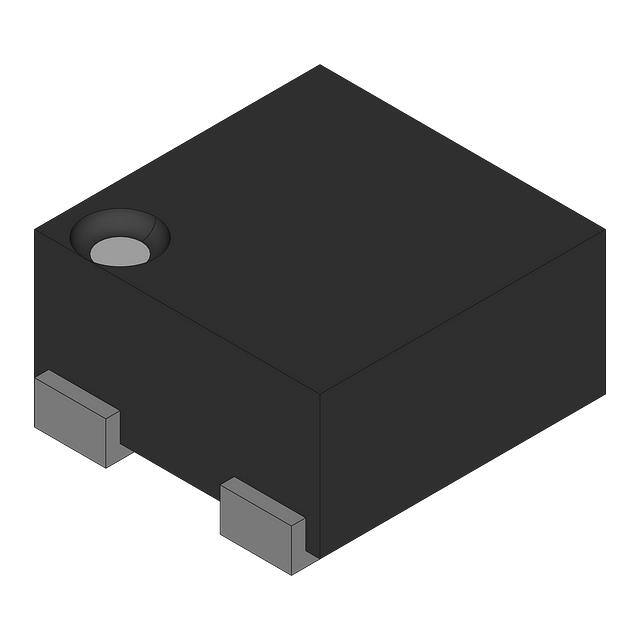
In addition to SOT-23-5, SC-88A and DFN1010-4 packages, a 0.8mm square ultra compact DFN(PLP)0808-4
package is also available.
FEATURES
Supply Current ............................................................. Typ. 50A
Standby Mode .............................................................. Typ. 0.1A
Dropout Voltage............................................................ Typ. 0.25V (IOUT150mA, VOUT2.5V)
Ripple Rejection ........................................................... Typ. 75dB (f1kHz, VOUT2.5V)
Temperature-Drift Coefficient of Output Voltage .......... Typ. 100ppm/C (VOUT1.8V)
Typ. 30ppm/C (VOUT≥1.8V)
Line Regulation ............................................................ Typ. 0.02%/V
Output Voltage Accuracy .............................................. 1.0%
Packages...................................................................... DFN(PLP)0808-4, DFN1010-4, SC-88A, SOT-23-5
Input Voltage Range ..................................................... 1.4V to 5.25V
Output Voltage Range .................................................. 0.8V to 3.6V (0.1V steps)
(For other voltages, please refer to MARK INFORMATIONS.)
Built-in Fold Back Protection Circuit ............................. Typ. 40mA (Current at short mode)
Ceramic capacitors are recommended to be used with this IC .... 0.1F or more
APPLICATIONS
Power source for portable communication equipment.
Power source for electrical appliances such as cameras, VCRs and camcorders.
Power source for battery-powered equipment.
Power source for home appliances.
1
�RP109x
NO.EA-204-170425
BLOCK DIAGRAMS
RP109xxxxB
RP109xxxxD
VDD
VOUT
VDD
VOUT
Vref
Vref
Current Limit
Current Limit
CE
GND CE
GND
SELECTION GUIDE
The output voltage, auto discharge function, package, and the taping type, etc. for the ICs can be selected at
the user’s request.
Product Name
Package
Quantity per Reel
Pb Free
Halogen Free
RP109Kxx1-TR
DFN(PLP)0808-4
10,000 pcs
Yes
Yes
RP109Lxx1-TR
DFN1010-4
10,000 pcs
Yes
Yes
RP109Qxx2-TR-FE
SC-88A
3,000 pcs
Yes
Yes
RP109Nxx1-TR-FE
SOT-23-5
3,000 pcs
Yes
Yes
xx: Specify the set output voltage (VSET) within the range of 0.8V to 3.6 in 0.1V steps.
The second decimal point of VSET is described as below.
1.25V: RP109x12x5
1.85V: RP109x18x5
2.85V: RP109x28x5
: Select the polarity of the CE pin from (B) "H" active without auto-discharge function or (D) "H" active with
auto-discharge function.
2
�RP109x
NO.EA-204-170425
PIN CONFIGURATIONS
DFN(PLP)0808-4
Top View
4
3
DFN1010-4
Bottom View
3
4
Top View
4
Bottom View
3
3
2
5
2
1
1
2
4
SOT-23-5
5
4
4
1
SC-88A
2
(mark side)
1
1
2
3
(mark side)
1
2
3
PIN DESCRIPTIONS
DFN(PLP)0808-4 / DFN1010-4
Pin No
Symbol
Pin Description
1
VOUT
Output Pin
2
GND
Ground Pin
3
CE
Chip Enable Pin ("H" Active)
4
VDD
Input Pin
Tab is GND level. (They are connected to the reverse side of this IC.)
The tab is better to be connected to the GND, but leaving it open is also acceptable.
SC-88A
Pin No
Symbol
Pin Description
1
CE
Chip Enable Pin ("H" Active)
2
NC
No Connection
3
GND
Ground Pin
4
VOUT
Output Pin
5
VDD
Input Pin
Pin No. 2 is connected to the bottom of the IC. It is recommended that the pin be connected to the ground plane on the
board, or otherwise be left floating so that there is no contact with other potentials.
SOT-23-5
Pin No
Symbol
Pin Description
1
VDD
2
GND
3
CE
Chip Enable Pin ("H" Active)
4
NC
No Connection
5
VOUT
Output Pin
Input Pin
Ground Pin
3
�RP109x
NO.EA-204-170425
ABSOLUTE MAXIMUM RATINGS
Symbol
Item
Rating
Unit
6.0
V
0.3 to 6.0
V
VIN
Input Voltage
VCE
Input Voltage (CE Pin)
VOUT
Output Voltage
0.3 to VIN0.3
V
IOUT
Output Current
180
mA
Power Dissipation (DFN(PLP)0808-4)
PD
Ta
Tstg
Power Dissipation
(DFN1010-4)
286
400
Power Dissipation (SC-88A)
380
Power Dissipation (SOT-23-5)
420
mW
Operating Temperature Range
40 to 85
C
Storage Temperature Range
55 to 125
C
) For Power Dissipation, please refer to PACKAGE INFORMATION.
ABSOLUTE MAXIMUM RATINGS
Electronic and mechanical stress momentarily exceeded absolute maximum ratings may cause the
permanent damages and may degrade the life time and safety for both device and system using the device
in the field.
The functional operation at or over these absolute maximum ratings is not assured.
4
�RP109x
NO.EA-204-170425
ELECTRICAL CHARACTERISTICS
RP109xxxxB/D
VIN=VSET+1.0V (VOUT>1.5), VIN=2.5V(VOUT≤1.5V), IOUT=1mA, CIN=COUT=0.1μF, unless otherwise noted.
The specifications surrounded by
are guaranteed by Design Engineering at -40ºC ≤ Ta ≤ 85 ºC.
RP109x Series
Symbol
(Ta=25C)
Item
Conditions
Ta= 25C
VOUT
Output Voltage
-40C ≤ Ta ≤ 85C
IOUT
Min.
Typ.
Max.
Unit
VSET ≥ 1.8V
x 0.99
x 1.01
V
VSET < 1.8V
-18
+18
mV
VSET ≥ 1.8V
x 0.985
x 1.015
V
VSET < 1.8V
-50
+50
mV
Output Current
mA
150
VOUT
/IOUT
Load Regulation
VDIF
Dropout Voltage
ISS
Supply Current
IOUT = 0mA
50
70
μA
Istandby
Supply Current
(Standby Mode)
VCE = 0V
0.1
1.0
μA
VOUT
/VIN
Line Regulation
VSET0.5V ≤ VIN ≤ 5.25V
VIN ≥ 1.4V
0.02
0.10
%/V
RR
Ripple Rejection
f = 1kHz
Ripple 0.2Vp-p
VIN = VSET +1.0V
IOUT = 30mA
VIN
Input Voltage*1
VOUT
/Ta
1mA ≤ IOUT ≤ 150mA
ISC
Short Current Limit
VOUT 0V
IPD
CE Pull-down Current
VCEH
CE Input Voltage “H”
VCEL
CE Input Voltage “L”
RLOW
Nch On Resistance
for Auto-discharge
(D Version Only)
75
1.4
-40C ≤ Ta ≤ 85C
Output Noise
30
mV
Please see Dropout Voltage on the next page.
Output Voltage
Temperature Coefficient
en
5
dB
5.25
VSET ≥ 1.8V
30
VSET < 1.8V
100
ppm
/C
40
mA
0.3
0.6
0.4
VIN = 4.0V
VCE = 0V
VSET ≥ 1.8V
VSET < 1.8V
μA
V
1.0
BW = 10Hz to
100kHz
V
V
20
x VSET
40
x VSET
μVrms
60
Ω
All test items listed under Electrical Characteristics are done under the pulse load condition (Tj≈Ta=25ºC) except
Output Noise, Ripple Rejection, and Output Voltage Temperature Coefficient.
*1
Maximum input voltage is 5.25V. If, for any reason the input voltage exceeds 5.25V, it has to be no more than
5.5V, and total operating time should be within 500 hours.
5
�RP109x
NO.EA-204-170425
The specifications surrounded by
are guaranteed by Design Engineering at -40ºC ≤ Ta ≤ 85 ºC.
(Ta=25C)
Dropout Voltage
Set Output Voltage
VSET (V)
Dropout Voltage
VDIF (V)
Condition
Typ.
Max.
VSET = 0.8
0.700
1.000
VSET = 0.9
0.620
0.910
1.0 ≤ VSET < 1.2
0.560
0.820
0.470
0.670
0.390
0.540
1.8 ≤ VSET < 2.1
0.330
0.480
2.1 ≤ VSET < 2.5
0.280
0.400
2.5 ≤ VSET < 3.0
0.250
0.350
3.0 ≤ VSET
3.6
0.230
0.320
1.2 ≤ VSET < 1.4
1.4 ≤ VSET < 1.8
IOUT = 150mA
RECOMMENDED OPERATING CONDITIONS (ELECTRICAL CHARACTERISTICS)
All of electronic equipment should be designed that the mounted semiconductor devices operate within the
recommended operating conditions. The semiconductor devices cannot operate normally over the
recommended operating conditions, even if when they are used over such conditions by momentary
electronic noise or surge. And the semiconductor devices may receive serious damage when they continue
to operate over the recommended operating conditions.
6
�RP109x
NO.EA-204-170425
TYPICAL APPLICATION
VDD
C1
CE Control
RP109x
Series
CE
VOUT
VOUT
C2
GND
(External Components)
C2 0.1F MURATA: GRM155B31C104KA87B
TECHNICAL NOTES
When using these ICs, consider the following points:
Phase Compensation
In these ICs, phase compensation is made for securing stable operation even if the load current is varied. For
this purpose, use a capacitor C2 with 0.1F or more and good ESR (Equivalent Series Resistance).
(Note: If additional ceramic capacitors are connected with parallel to the output pin with an output capacitor for
phase compensation, the operation might be unstable. Because of this, test these ICs with as same external
components as ones to be used on the PCB.)
PCB Layout
Make VDD and GND lines sufficient. If their impedance is high, noise pickup or unstable operation may result.
Connect a capacitor C1 with a capacitance value as much as 0.1F or more between VDD and GND pin, and as
close as possible to the pins.
Set external components, especially the output capacitor C2, as close as possible to the ICs, and make wiring
as short as possible.
7
�RP109x
NO.EA-204-170425
PACKAGE INFORMATION
Power Dissipation (DFN (PLP) 0808-4)
Power Dissipation (PD) depends on conditions of mounting on board. This specification is based on the
measurement at the condition below:
Measurement Conditions:
Standard Land Pattern
Environment
Mounting on Board (Wind velocity=0m/s)
Board Material
Glass cloth epoxy plastic (Double-sided)
Board Dimensions
40mm 40mm 1.6mm
Copper Ratio
Top side: Approx. 50%, Back side: Approx. 50%
Through-holes
0.5mm 24pcs
Measurement Results:
(Ta=25C)
Standard Land Pattern
286mW (Tjmax=125C)
358mW (Tjmax=150C)
ja = (125-25C)/0.286W= 350C/W
Power Dissipation
400
jc= 90C/W
40
358
350
300
286
250
200
40
Power Dissipation PD (mW)
Thermal Resistance
150
100
50
0
0
25
50
75 85 100
125
150
Measurement Board Pattern
Ambient Temperature (°C)
Power Dissipation
IC Mount Area (Unit: mm)
The above graph shows the Power Dissipation of the package under the conditions of Tjmax=125C
and Tjmax=150C.
The operation of the IC within the shaded range in the graph might have an affect on the IC’s lifetime.
The operation time of the IC must be remained within the time limit described in the table below.
Estimated Years
Operating Time
(Operating 4 hours/day)
13,000 hours
9 years
8
�RP109x
NO.EA-204-170425
Package Dimensions (DFN (PLP) 0808-4)
0.48
3
X4
0.80
0.05
4
0.25
0.05
45
※
0.220.05
B
0.280.05
A
0.80
C0.16
S
0.060.05
0.4max
0.05min
INDEX
2
1
0.25
0.05
0.220.05
0.05
Bottom View
M
S AB
(Unit : mm)
※) Tab is GND level. (They are connected to the
reverse side of this IC.)
The tab is better to be connected to the GND,
but leaving it open is also acceptable.
0.05 S
Mark Specification (DFN (PLP) 0808-4)
: Product Code … Refer to “RP109K Series Mark Specification Table”.
: Lot Number … Alphanumeric Serial Number
①②
③
9
�RP109x
NO.EA-204-170425
RP109K Series Mark Specification Table (DFN(PLP)0808-4)
RP109Kxx1B
Product Name
RP109K081B
RP109K091B
RP109K101B
RP109K111B
RP109K121B
RP109K131B
RP109K141B
RP109K151B
RP109K161B
RP109K171B
RP109K181B
RP109K191B
RP109K201B
RP109K211B
RP109K221B
RP109K231B
RP109K241B
RP109K251B
RP109K261B
RP109K271B
RP109K281B
RP109K291B
RP109K301B
RP109K311B
RP109K321B
RP109K331B
RP109K341B
RP109K351B
RP109K361B
RP109K121B5
RP109K181B5
RP109K281B5
10
RP109Kxx1D
A
A
A
A
A
A
A
A
A
A
A
A
A
A
A
A
A
A
A
A
A
A
A
A
A
A
A
A
A
A
A
A
VSET
0.8V
0.9V
1.0V
1.1V
1.2V
1.3V
1.4V
1.5V
1.6V
1.7V
1.8V
1.9V
2.0V
2.1V
2.2V
2.3V
2.4V
2.5V
2.6V
2.7V
2.8V
2.9V
3.0V
3.1V
3.2V
3.3V
3.4V
3.5V
3.6V
1.25V
1.85V
2.85V
Product Name
RP109K081D
RP109K091D
RP109K101D
RP109K111D
RP109K121D
RP109K131D
RP109K141D
RP109K151D
RP109K161D
RP109K171D
RP109K181D
RP109K191D
RP109K201D
RP109K211D
RP109K221D
RP109K231D
RP109K241D
RP109K251D
RP109K261D
RP109K271D
RP109K281D
RP109K291D
RP109K301D
RP109K311D
RP109K321D
RP109K331D
RP109K341D
RP109K351D
RP109K361D
RP109K121D5
RP109K181D5
RP109K281D5
A
A
A
A
A
A
A
A
A
A
A
A
A
A
A
A
A
A
A
A
A
A
A
A
A
A
A
A
A
A
A
A
VSET
0.8V
0.9V
1.0V
1.1V
1.2V
1.3V
1.4V
1.5V
1.6V
1.7V
1.8V
1.9V
2.0V
2.1V
2.2V
2.3V
2.4V
2.5V
2.6V
2.7V
2.8V
2.9V
3.0V
3.1V
3.2V
3.3V
3.4V
3.5V
3.6V
1.25V
1.85V
2.85V
�RP109x
NO.EA-204-170425
Power Dissipation (DFN1010-4)
Power Dissipation (PD) depends on conditions of mounting on board. This specification is based on the
measurement at the condition below:
Measurement Conditions:
Standard Land Pattern
Environment
Mounting on Board (Wind velocity=0m/s)
Board Material
Glass cloth epoxy plastic (Double sided)
Board Dimensions
40mm 40mm 1.6mm
Copper Ratio
Top side: Approx. 50%, Back side: Approx. 50%
Through-holes
0.54mm 24pcs
Measurement Results:
(Ta=25C)
Standard Land Pattern
400mW (Tjmax=125C)
500mW (Tjmax=150C)
ja = (125-25C)/0.4W= 250C/W
Power Dissipation
Thermal Resistance
jc= 67C/W
40
500
500
400
400
300
40
Power Dissipation PD (mW)
600
200
100
0
0
25
50
75 85 100
125
150
Measurement Board Pattern
Ambient Temperature (°C)
IC Mount Area (Unit: mm)
Power Dissipation
The above graph shows the Power Dissipation of the package under the conditions of Tjmax=125C
and Tjmax=150C.
The operation of the IC within the shaded range in the graph might have an affect on the IC’s lifetime.
The operation time of the IC must be remained within the time limit described in the table below.
Operating Time
13,000 hours
Estimated Years
(Operating 4 hours/day)
9 years
11
�RP109x
NO.EA-204-170425
Package Dimensions (DFN1010-4)
A
1.00
0.250.05
B
0.65
3
X4
*
0.05
1.00
45
0.4max.
0.48 2
0.05
+0.08
0.1-0.03
4-C0.157
C0.12
INDEX
S
4
1 0.48
0.05
0.220.05
0.05 M AB
Bottom View
0.05 S
*) Tab is GND level. (They are connected to the
reverse side of this IC.)
The tab is better to be connected to the GND,
but leaving it open is also acceptable.
Mark Specification (DFN1010-4)
: Product Code …Refer to “RP109L Series Mark Specification Table”.
: Lot Number … Alphanumeric Serial Number
①②
③④
12
(Unit : mm)
�RP109x
NO.EA-204-170425
RP109L Series Mark Specification Table (DFN1010-4)
RP109Lxx1B
Product Name
RP109L081B
RP109L091B
RP109L101B
RP109L111B
RP109L121B
RP109L131B
RP109L141B
RP109L151B
RP109L161B
RP109L171B
RP109L181B
RP109L191B
RP109L201B
RP109L211B
RP109L221B
RP109L231B
RP109L241B
RP109L251B
RP109L261B
RP109L271B
RP109L281B
RP109L291B
RP109L301B
RP109L311B
RP109L321B
RP109L331B
RP109L341B
RP109L351B
RP109L361B
RP109L121B5
RP109L181B5
RP109L281B5
RP109Lxx1D
C0
C1
C2
C3
C4
C5
C6
C7
C8
C9
D0
D1
D2
D3
D4
D5
D6
D7
D8
D9
E0
E1
E2
E3
E4
E5
E6
E7
E8
E9
J0
J1
VSET
0.8V
0.9V
1.0V
1.1V
1.2V
1.3V
1.4V
1.5V
1.6V
1.7V
1.8V
1.9V
2.0V
2.1V
2.2V
2.3V
2.4V
2.5V
2.6V
2.7V
2.8V
2.9V
3.0V
3.1V
3.2V
3.3V
3.4V
3.5V
3.6V
1.25V
1.85V
2.85V
Product Name
RP109L081D
RP109L091D
RP109L101D
RP109L111D
RP109L121D
RP109L131D
RP109L141D
RP109L151D
RP109L161D
RP109L171D
RP109L181D
RP109L191D
RP109L201D
RP109L211D
RP109L221D
RP109L231D
RP109L241D
RP109L251D
RP109L261D
RP109L271D
RP109L281D
RP109L291D
RP109L301D
RP109L311D
RP109L321D
RP109L331D
RP109L341D
RP109L351D
RP109L361D
RP109L121D5
RP109L181D5
RP109L281D5
F0
F1
F2
F3
F4
F5
F6
F7
F8
F9
G0
G1
G2
G3
G4
G5
G6
G7
G8
G9
H0
H1
H2
H3
H4
H5
H6
H7
H8
H9
K0
K1
VSET
0.8V
0.9V
1.0V
1.1V
1.2V
1.3V
1.4V
1.5V
1.6V
1.7V
1.8V
1.9V
2.0V
2.1V
2.2V
2.3V
2.4V
2.5V
2.6V
2.7V
2.8V
2.9V
3.0V
3.1V
3.2V
3.3V
3.4V
3.5V
3.6V
1.25V
1.85V
2.85V
13
�RP109x
NO.EA-204-170425
Power Dissipation (SC-88A)
Power Dissipation (PD) depends on conditions of mounting on board. This specification is based on the
measurement at the condition below:
Measurement Conditions:
Standard Land Pattern
Environment
Mounting on Board (Wind velocity=0m/s)
Board Material
Glass cloth epoxy plastic (Double Layers)
Board Dimensions
40mm 40mm 1.6mm
Copper Ratio
Top side: Approx. 50%, Back side: Approx. 50%
Through-hole
0.5mm 44pcs
Measurement Results:
(Ta=25C)
Standard Land Pattern
Power Dissipation
Thermal Resistance
Free Air
380mW (Tjmax=125C)
475mW (Tjmax=150C)
ja=(125-25C)/0.38W=263C/W
ja=(125-25C)/0.15W=667C/W
jc=75C/W
-
150mW
40
475
500
On Board
400
Free Air
380
300
40
Power Dissipation PD (mW)
600
200
150
100
0
0
25
50
75 85 100
125
150
Measurement Board Pattern
Ambient Temperature (°C)
IC Mount Area (Unit: mm)
Power Dissipation
The above graph shows the Power Dissipation of the package under the conditions of Tjmax=125C and
Tjmax=150C.
The operation of the IC within the shaded range in the graph might have an affect on the IC’s lifetime. The
operation time of the IC must be remained within the time limit described in the table below.
Operating Time
13,000 hours
14
Estimated Years
(Operating 4 hours/day)
9 years
�RP109x
NO.EA-204-170425
Package Dimensions (SC-88A)
2.0±0.2
0.15±0.07
B
1.3±0.2
4
+0.2
1.25 -0.1
5
0.15
2.1±0.3
A
0.36±0.1
0~14
2
3
+0.1
0.65
+0.1
S
0.10 S AB
0~0.1
0.9 -0.2
0.2 -0.05
1.1Max.
1
0.10 S
Unit : mm
Mark Specification (SC-88A)
: Product Code …Refer to “RP109Q Series Mark Specification Table”.
: Lot Number … Alphanumeric Serial Number
5
4
①②③
④⑤⑥
1
2
3
15
�RP109x
NO.EA-204-170425
RP109Q Series Mark Specification Table (SC-88A)
RP109Qxx2B
Product Name
RP109Q082B
RP109Q092B
RP109Q102B
RP109Q112B
RP109Q122B
RP109Q132B
RP109Q142B
RP109Q152B
RP109Q162B
RP109Q172B
RP109Q182B
RP109Q192B
RP109Q201B
RP109Q212B
RP109Q222B
RP109Q232B
RP109Q242B
RP109Q252B
RP109Q262B
RP109Q272B
RP109Q282B
RP109Q292B
RP109Q302B
RP109Q312B
RP109Q322B
RP109Q332B
RP109Q342B
RP109Q352B
RP109Q362B
RP109Q122B5
RP109Q182B5
RP109Q282B5
16
RP109Qxx2D
AE08
AE09
AE10
AE11
AE12
AE13
AE14
AE15
AE16
AE17
AE18
AE19
AE20
AE21
AE22
AE23
AE24
AE25
AE26
AE27
AE28
AE29
AE30
AE31
AE32
AE33
AE34
AE35
AE36
AE37
AE38
AE39
VSET
0.8V
0.9V
1.0V
1.1V
1.2V
1.3V
1.4V
1.5V
1.6V
1.7V
1.8V
1.9V
2.0V
2.1V
2.2V
2.3V
2.4V
2.5V
2.6V
2.7V
2.8V
2.9V
3.0V
3.1V
3.2V
3.3V
3.4V
3.5V
3.6V
1.25V
1.85V
2.85V
Product Name
RP109Q082D
RP109Q092D
RP109Q102D
RP109Q112D
RP109Q122D
RP109Q132D
RP109Q142D
RP109Q152D
RP109Q162D
RP109Q172D
RP109Q182D
RP109Q192D
RP109Q202D
RP109Q212D
RP109Q222D
RP109Q232D
RP109Q242D
RP109Q252D
RP109Q262D
RP109Q272D
RP109Q282D
RP109Q292D
RP109Q302D
RP109Q312D
RP109Q322D
RP109Q332D
RP109Q342D
RP109Q352D
RP109Q362D
RP109Q122D5
RP109Q182D5
RP109Q282D5
AF08
AF09
AF10
AF11
AF12
AF13
AF14
AF15
AF16
AF17
AF18
AF19
AF20
AF21
AF22
AF23
AF24
AF25
AF26
AF27
AF28
AF29
AF30
AF31
AF32
AF33
AF34
AF35
AF36
AF37
AF38
AF39
VSET
0.8V
0.9V
1.0V
1.1V
1.2V
1.3V
1.4V
1.5V
1.6V
1.7V
1.8V
1.9V
2.0V
2.1V
2.2V
2.3V
2.4V
2.5V
2.6V
2.7V
2.8V
2.9V
3.0V
3.1V
3.2V
3.3V
3.4V
3.5V
3.6V
1.25V
1.85V
2.85V
�RP109x
NO.EA-204-170425
Power Dissipation (SOT-23-5)
Power Dissipation (PD) depends on conditions of mounting on board. This specification is based on the
measurement at the condition below:
(Power Dissipation (SOT-23-5) is substitution of SOT-23-6.)
Measurement Conditions:
Standard Land Pattern
Environment
Mounting on Board (Wind velocity=0m/s)
Board Material
Glass cloth epoxy plastic (Double sided)
Board Dimensions
40mm 40mm 1.6mm
Copper Ratio
Top side: Approx. 50%, Back side: Approx. 50%
Through-holes
0.5mm 44pcs
Measurement Results:
(Ta=25C)
Standard Land Pattern
420mW (Tjmax=125C)
525mW (Tjmax=150C)
ja = (125-25C)/0.42W= 238C/W
Power Dissipation
Thermal Resistance
Free Air
250mW
400C/W
40
525
On Board
500
400
420
300
250
Free Air
40
Power Dissipation PD (mW)
600
200
100
0
0
25
50
75 85 100
Ambient Temperature (°C)
Power Dissipation
125
150
Measurement Board Pattern
IC Mount Area (Unit: mm)
The above graph shows the Power Dissipation of the package under the conditions of Tjmax=125C
and Tjmax=150C.
The operation of the IC within the shaded range in the graph might have an affect on the IC’s lifetime.
The operation time of the IC must be remained within the time limit described in the table below.
Estimated Years
Operating Time
(Operating 4 hours/day)
13,000 hours
9 years
17
�RP109x
NO.EA-204-170425
Package Dimensions (SOT-23-5)
2.9±0.2
1.1±0.1
1.9±0.2
0.8±0.1
(0.95)
4
1
2
0~0.1
0.2min.
+0.2
1.6-0.1
5
2.8±0.3
(0.95)
3
+0.1
0.15-0.05
0.4±0.1
Unit : mm
Mark Specification (SOT-23-5)
: Product Code …Refer to “RP109N Mark Specification Table”.
: Lot Number … Alphanumeric Serial Number
5
4
1
18
2
3
�RP109x
NO.EA-204-170425
RP109N Series Mark Specification Table (SOT-23-5)
RP109Nxx1B
Product Name
RP109N081B
RP109N091B
RP109N101B
RP109N111B
RP109N121B
RP109N131B
RP109N141B
RP109N151B
RP109N161B
RP109N171B
RP109N181B
RP109N191B
RP109N201B
RP109N211B
RP109N221B
RP109N231B
RP109N241B
RP109N251B
RP109N261B
RP109N271B
RP109N281B
RP109N291B
RP109N301B
RP109N311B
RP109N321B
RP109N331B
RP109N341B
RP109N351B
RP109N361B
RP109N121B5
RP109N181B5
RP109N281B5
RP109Nxx1D
NAA
NAB
NAC
NAD
NAE
NAF
NAG
NAH
NAJ
NAK
NAL
NAM
NAN
NAP
NAQ
NAR
NAS
NAT
NAU
NAV
NAW
NAX
NAY
NAZ
PAA
PAB
PAC
PAD
PAE
PAF
PAG
PAH
VSET
0.8V
0.9V
1.0V
1.1V
1.2V
1.3V
1.4V
1.5V
1.6V
1.7V
1.8V
1.9V
2.0V
2.1V
2.2V
2.3V
2.4V
2.5V
2.6V
2.7V
2.8V
2.9V
3.0V
3.1V
3.2V
3.3V
3.4V
3.5V
3.6V
1.25V
1.85V
2.85V
Product Name
RP109N081D
RP109N091D
RP109N101D
RP109N111D
RP109N121D
RP109N131D
RP109N141D
RP109N151D
RP109N161D
RP109N171D
RP109N181D
RP109N191D
RP109N201D
RP109N211D
RP109N221D
RP109N231D
RP109N241D
RP109N251D
RP109N261D
RP109N271D
RP109N281D
RP109N291D
RP109N301D
RP109N311D
RP109N321D
RP109N331D
RP109N341D
RP109N351D
RP109N361D
RP109N121D5
RP109N181D5
RP109N281D5
NBA
NBB
NBC
NBD
NBE
NBF
NBG
NBH
NBJ
NBK
NBL
NBM
NBN
NBP
NBQ
NBR
NBS
NBT
NBU
NBV
NBW
NBX
NBY
NBZ
PBA
PBB
PBC
PBD
PBE
PBF
PBG
PBH
VSET
0.8V
0.9V
1.0V
1.1V
1.2V
1.3V
1.4V
1.5V
1.6V
1.7V
1.8V
1.9V
2.0V
2.1V
2.2V
2.3V
2.4V
2.5V
2.6V
2.7V
2.8V
2.9V
3.0V
3.1V
3.2V
3.3V
3.4V
3.5V
3.6V
1.25V
1.85V
2.85V
19
�RP109x
NO.EA-204-170425
TEST CIRCUITS
VDD
VOUT
RP109x
Series
C1
CE
C2
V
VOUT
IOUT
GND
C1=Ceramic 0.1F
C2=Ceramic 0.1F
Basic Test Circuit
VDD
A
RP109x
Series
C1
ISS
VOUT
VOUT
CE
C2
GND
C1=Ceramic 0.1F
C2=Ceramic 0.1F
Test Circuit for Supply Current
Pulse
Generator
VDD
VOUT
RP109x
Series
P.G.
CE
C2
IOUT
GND
C2=Ceramic 0.1F
Test Circuit for Ripple Rejection
VDD
C1
RP109x
Series
CE
VOUT
VOUT
C2
GND
IOUTa
IOUTb
C1=Ceramic 0.1F
C2=Ceramic 0.1F
Test Circuit for Load Transient Response
20
�RP109x
NO.EA-204-170425
TYPICAL CHARACTERISTICS
1) Output Voltage vs. Output Current (C10.1F, C20.1F, Topt25C)
RP109x08xx
0.9
RP109x17xx
1.8
1.6
0.7
0.6
0.5
0.4
VIN=1.4V
VIN=1.5V
VIN=1.6V
VIN=1.8V
VIN=2.8V
VIN=3.8V
VIN=4.8V
VIN=5.25V
0.3
0.2
0.1
0
0
Output Voltage VOUT (V)
Output Voltage VOUT (V)
0.8
1.4
VIN=2.2V
1.2
VIN=2.7V
VIN=4.7V
VIN=5.25V
0.8
0.6
0.4
0.2
0
0
50 100 150 200 250 300 350
Output Current IOUT (mA)
50
100 150 200 250 300 350
Output Current IOUT (mA)
RP109x18xx
2.0
VIN=3.7V
1.0
RP109x25xx
3.0
1.6
VIN=2.2V
1.4
VIN=2.8V
1.2
VIN=3.8V
1.0
VIN=4.8V
VIN=5.25V
0.8
0.6
0.4
Output Voltage VOUT (V)
Output Voltage VOUT (V)
1.8
2.5
2.0
VIN=2.8V
VIN=3.5V
1.5
VIN=4.5V
VIN=5.25V
1.0
0.5
0.2
0
0
0
50
100 150 200 250 300 350
Output Current IOUT (mA)
0
50
100 150 200 250 300 350
Output Current IOUT (mA)
RP109x36xx
4.0
Output Voltage VOUT (V)
3.5
3.0
2.5
2.0
VIN=3.8V
1.5
VIN=4.6V
VIN=5.25V
1.0
0.5
0
0
50
100 150 200 250 300 350
Output Current IOUT (mA)
21
�RP109x
NO.EA-204-170425
2) Output Voltage vs. Input Voltage (C10.1F, C20.1F, Topt25C)
RP109x08xx
0.9
0.8
1.4
Output Voltage VOUT (V)
Output Voltage VOUT (V)
RP109x14xx
1.6
0.7
0.6
0.5
0.4
IOUT=1mA
0.3
IOUT=30mA
0.2
IOUT=50mA
1.2
1.0
0.8
0.2
0
0
1
2
3
4
IOUT=30mA
0.4
0.1
0
IOUT=1mA
0.6
IOUT=50mA
5
0
1
1.8
2.0
1.6
1.8
1.4
1.2
1.0
0.8
IOUT=1mA
0.6
IOUT=30mA
IOUT=50mA
0.2
5
1.4
1.2
1.0
IOUT=1mA
0.8
IOUT=30mA
0.6
IOUT=50mA
0.4
0.2
0
0
1
2
3
4
0
5
1
2
Input Voltage VIN (V)
3
4
5
Input Voltage VIN (V)
RP109x25xx
RP109x36xx
4.0
3.0
3.5
2.5
2.0
1.5
IOUT=1mA
IOUT=30mA
1.0
IOUT=50mA
0.5
Output Voltage VOUT (V)
Output Voltage VOUT (V)
4
1.6
0
3.0
2.5
2.0
IOUT=1mA
1.5
IOUT=30mA
1.0
IOUT=50mA
0.5
0
0
0
1
2
3
4
Input Voltage VIN (V)
22
3
RP109x18xx
Output Voltage VOUT (V)
Output Voltage VOUT (V)
RP109x17xx
0.4
2
Input Voltage VIN (V)
Input Voltage VIN (V)
5
0
1
2
3
4
Input Voltage VIN (V)
5
�RP109x
NO.EA-204-170425
3) Supply Current vs. Input Voltage (C10.1F, C20.1F, Topt25C)
RP109x08xx
60
RP109x14xx
100
90
80
Supply Current ISS (µA)
Supply Current ISS (µA)
50
40
30
20
70
60
50
40
30
20
10
10
0
0
0
1
2
3
4
5
0
1
Input Voltage VIN (V)
RP109x17xx
120
120
Supply Current ISS (µA)
Supply Current ISS (µA)
5
RP109x18xx
140
100
80
60
40
100
80
60
40
20
20
0
0
0
1
2
3
4
0
5
1
RP109x25xx
120
2
3
4
5
Input Voltage VIN (V)
Input Voltage VIN (V)
RP109x36xx
120
100
100
Supply Current ISS (µA)
Supply Current ISS (µA)
2
3
4
Input Voltage VIN (V)
80
60
40
20
80
60
40
20
0
0
0
1
2
3
4
Input Voltage VIN (V)
5
0
1
2
3
4
5
Input Voltage VIN (V)
23
�RP109x
NO.EA-204-170425
4) Output Voltage vs. Temperature (C10.1F, C20.1F, IOUT1mA)
RP109x08xx
VIN=1.8V
0.84
1.44
0.83
1.43
0.82
0.81
0.80
0.79
0.78
0.77
RP109x14xx
1.45
Output Voltage VOUT (V)
Output Voltage VOUT (V)
0.85
0.76
1.42
1.41
1.40
1.39
1.38
1.37
1.36
0.75
1.35
-50
-25
0
25
50
75
100
-50
-25
Temperature Topt (°C)
RP109x17xx
25
50
RP109x18xx
VIN=2.7V
1.85
1.74
1.84
1.73
1.83
1.72
1.71
1.70
1.69
1.68
1.67
1.66
75
100
VIN=2.8V
1.82
1.81
1.80
1.79
1.78
1.77
1.76
1.65
1.75
-50
-25
0
25
50
75
100
-50
-25
Temperature Topt (°C)
RP109x25xx
2.55
0
25
50
75
100
Temperature Topt (°C)
VIN=3.5V
2.54
3.64
2.53
3.63
2.52
2.51
2.50
2.49
2.48
2.47
2.46
RP109x36xx
3.65
Output Voltage VOUT (V)
Output Voltage VOUT (V)
0
Temperature Topt (°C)
Output Voltage VOUT (V)
Output Voltage VOUT (V)
1.75
VIN=4.6V
3.62
3.61
3.60
3.59
3.58
3.57
3.56
2.45
3.55
-50
-25
0
25
50
Temperature Topt (°C)
24
VIN=2.4V
75
100
-50
-25
0
25
50
Temperature Topt (°C)
75
100
�RP109x
NO.EA-204-170425
5) Supply Current vs. Temperature (C10.1F, C20.1F, IOUT0mA)
RP109x08xx
55
50
45
VIN=2.4V
60
Supply Current ISS (μA)
Supply Current ISS (μA)
60
RP109x14xx
VIN=1.8V
55
50
45
40
40
-50
-25
0
25
50
Temperature Topt (°C)
75
-50
100
-25
VIN=2.7V
75
100
VIN=2.8V
60
Supply Current ISS (μA)
Supply Current ISS (μA)
50
RP109x18xx
55
50
45
40
55
50
45
40
-50
-25
0
25
50
75
Temperature Topt (°C)
100
-50
-25
RP109x25xx
0
25
50
75
Temperature Topt (°C)
100
RP109x36xx
VIN=3.5V
55
50
45
40
VIN=4.6V
60
Supply Current ISS (μA)
60
Supply Current ISS (μA)
25
Temperature Topt (°C)
RP109x17xx
60
0
55
50
45
40
-50
-25
0
25
50
75
Temperature Topt (°C)
100
-50
-25
0
25
50
75
Temperature Topt (°C)
100
25
�RP109x
NO.EA-204-170425
6) Dropout Voltage vs. Output Current (C10.1F, C20.1F)
RP109x08xx
800
450
Dropout Voltage VDIF (mV)
700
Dropout Voltage VDIF (mV)
RP109x14xx
500
600
500
400
-40°C
300
25°C
200
85°C
100
400
350
300
250
200
150
-40°C
25°C
85°C
100
50
0
0
0
25
50
75
100
125
150
0
Output Current IOUT (mA)
RP109x25xx
50
75
100 125
Output Current IOUT (mA)
250
200
150
100
-40°C
25°C
85°C
50
0
200
150
100
-40°C
25°C
85°C
50
0
0
25
50
75
100
125
150
0
Output Current IOUT (mA)
25
50
75
RP109x
Dropout Voltage VDIF (mV)
600
10mA
30mA
50mA
150mA
500
400
300
200
100
0
0.4
26
0.8 1.2 1.6 2.0 2.4 2.8 3.2 3.6
Set Output Voltage VREG (V)
100
125
Output Current IOUT (mA)
7) Dropout Voltage vs. Set Output Voltage (C10.1F, C20.1F, Topt25C)
700
150
RP109x36xx
250
Dropout Voltage VDIF (mV)
Dropout Voltage VDIF (mV)
300
25
4.0
150
�RP109x
NO.EA-204-170425
8) Ripple Rejection vs. Input Bias Voltage (C1none, C20.1F, Ripple0.2Vp-p, Topt25C)
RP109x08xx IOUT=1mA
90
90
80
80
70
60
50
40
f=100Hz
f=1kHz
f=10kHz
f=100kHz
30
20
10
70
60
50
40
20
10
0
0.5 1.0 1.5 2.0 2.5 3.0 3.5 4.0 4.5 5.0 5.5
0.5 1.0 1.5 2.0 2.5 3.0 3.5 4.0 4.5 5.0 5.5
Input Voltage VIN (V)
RP109x14xx
IOUT=1mA
RP109x14xx
100
90
80
80
Ripple Rejection RR (dB)
Ripple Rejection RR (dB)
Input Voltage VIN (V)
90
70
60
50
40
f=100Hz
f=1kHz
f=10kHz
f=100kHz
30
20
10
f=100Hz
f=1kHz
f=10kHz
f=100kHz
30
0
100
RP109x08xx IOUT=30mA
100
Ripple Rejection RR (dB)
Ripple Rejection RR (dB)
100
70
60
50
40
f=100Hz
f=1kHz
f=10kHz
f=100kHz
30
20
10
0
0
1.0 1.5 2.0 2.5 3.0 3.5 4.0 4.5 5.0 5.5
1.0 1.5 2.0 2.5 3.0 3.5 4.0 4.5 5.0 5.5
Input Voltage VIN (V)
Input Voltage VIN (V)
RP109x25xx
RP109x25xx
IOUT=1mA
100
100
90
90
80
80
Ripple Rejection RR (dB)
Ripple Rejection RR (dB)
IOUT=30mA
70
60
50
40
f=100Hz
f=1kHz
f=10kHz
f=100kHz
30
20
10
IOUT=30mA
70
60
50
40
f=100Hz
f=1kHz
f=10kHz
f=100kHz
30
20
10
0
0
2.5
3.0
3.5
4.0
4.5
Input Voltage VIN (V)
5.0
5.5
2.5
3.0
3.5
4.0
4.5
Input Voltage VIN (V)
5.0
5.5
27
�RP109x
NO.EA-204-170425
RP109x36xx
RP109x36xx
IOUT=1mA
100
100
90
Ripple Rejection RR (dB)
90
Ripple Rejection RR (dB)
IOUT=30mA
80
70
60
50
40
f=100Hz
f=1kHz
f=10kHz
f=100kHz
30
20
10
80
70
60
50
40
f=100Hz
f=1kHz
f=10kHz
f=100kHz
30
20
10
0
0
3.5
4.0
4.5
5.0
5.5
3.5
4.0
4.5
5.0
5.5
Input Voltage VIN (V)
Input Voltage VIN (V)
9) Ripple Rejection vs. Frequency (C1none, C20.1F, Ripple0.2Vp-p)
RP109x08xx
VIN=1.8V
RP109x14xx
100
90
90
80
80
Ripple Rejection RR (dB)
Ripple Rejection RR (dB)
100
70
60
50
40
1mA
30
30mA
150mA
20
70
60
50
40
20
10
0
0
0.1
1
10
100
Frequency f (kHz)
RP109x17xx
100
1000
VIN=2.7V
0.1
90
80
80
60
50
40
1mA
30mA
150mA
30
20
50
40
20
0
1000
1mA
30mA
150mA
30
0
10
100
Frequency f (kHz)
VIN=2.8V
60
10
1
1000
70
10
0.1
10
100
Frequency f (kHz)
RP109x18xx
90
70
1
100
Ripple Rejection RR (dB)
Ripple Rejection RR (dB)
1mA
30mA
150mA
30
10
28
VIN=2.4V
0.1
1
10
100
Frequency f (kHz)
1000
�RP109x
NO.EA-204-170425
RP109x25xx
RP109x36xx
VIN=3.5V
100
90
90
80
80
Ripple Rejection RR (dB)
Ripple Rejection RR (dB)
100
70
60
50
40
1mA
30
30mA
20
150mA
VIN=4.6V
70
60
50
40
1mA
30
30mA
20
150mA
10
10
0
0
0.1
1
10
100
Frequency f (kHz)
0.1
1000
1
10
100
Frequency f (kHz)
1000
10) Input Transient Response (C1none, C20.1F, IOUT30mA, trtf5s, Topt25C)
3.5
2.0
Input Voltage
1.82.8V
1.5
1.0
0.805
0.800
Output Voltage
0.795
Output Voltage VOUT (V)
4.0
2.5
0.790
Input Voltage
2.43.4V
2.5
2.0
1.405
1.400
Output Voltage
1.395
1.390
0.785
1.385
20 40 60 80 100 120 140 160 180 200
0
Time t (µs)
RP109x17xx
RP109x18xx
2.5
2.0
1.700
Output Voltage
1.690
Output Voltage VOUT (V)
3.5
Input Voltage VIN (V)
4.0
3.5
1.705
1.695
Time t (µs)
4.0
3.0
Input Voltage
2.73.7V
20 40 60 80 100 120 140 160 180 200
3.0
Input Voltage
2.83.8V
2.5
2.0
1.805
1.800
Output Voltage
1.795
Input Voltage VIN (V)
0
Output Voltage VOUT (V)
3.0
Input Voltage VIN (V)
RP109x14xx
3.0
Input Voltage VIN (V)
Output Voltage VOUT (V)
RP109x08xx
1.790
1.685
1.785
0
20 40 60 80 100 120 140 160 180 200
Time t (µs)
0
20 40 60 80 100 120 140 160 180 200
Time t (µs)
29
�RP109x
NO.EA-204-170425
RP109x36xx
5.0
6.0
3.5
3.0
2.505
2.500
Output Voltage
2.495
2.490
Output Voltage VOUT (V)
4.0
Input Voltage
3.54.5V
5.5
Input Voltage VIN (V)
Output Voltage VOUT (V)
4.5
5.0
Input Voltage
4.65.6V
4.5
4.0
3.605
3.600
3.595
Output Voltage
Input Voltage VIN (V)
RP109x25xx
3.590
2.485
0
20 40
3.585
60 80 100 120 140 160 180 200
0
20 40 60 80 100 120 140 160 180 200
Time t (µs)
Time t (µs)
11) Load Transient Response (C10.1F, C20.1F, trtf5s, Topt25C)
100
0
0.80
Output Voltage
0.76
50
Output Current
50mA100mA
1.44
0
1.42
1.40
1.38
Output Voltage
1.36
0.74
1.34
20
40
60
80
100
0
20
40
Time t (µs)
RP109x17xx
60
80
Time t (µs)
VIN=2.7V
RP109x18xx
200
VIN=2.8V
0
1.74
1.72
1.70
Output Voltage
Output Voltage VOUT (V)
50
Output Current
50mA100mA
Output Current IOUT (mA)
Output Voltage VOUT (V)
100
100
1.80
1.78
1.64
1.74
40
60
Time t (µs)
80
100
0
1.82
1.76
20
50
Output Current
50mA100mA
1.84
1.66
0
200
150
150
1.68
100
Output Voltage
0
20
40
60
Time t (µs)
80
100
Output Current IOUT (mA)
0
30
Output Current IOUT (mA)
100
0.82
0.78
200
150
Output Voltage VOUT (V)
0.84
VIN=2.4V
150
50
Output Current
50mA100mA
RP109x14xx
200
Output Current IOUT (mA)
Output Voltage VOUT (V)
RP109x08xx VIN=1.8V
�RP109x
NO.EA-204-170425
RP109x36xx
200
VIN=4.6V
200
50
Output Current
50mA100mA
0
2.52
2.50
Output Voltage
2.48
100
50
Output Current
50mA100mA
3.62
3.60
3.58
2.46
3.56
2.44
3.54
0
20
40
60
80
100
Output Voltage
0
20
Time t (µs)
RP109x08xx
0
40
60
80
100
Time t (µs)
VIN=1.8V
RP109x14xx
200
VIN=2.4V
200
100
50
0
Output Current
1mA150mA
1.0
0.9
0.8
0.7
Output Voltage
Output Voltage VOUT (V)
150
Output Current IOUT (mA)
Output Voltage VOUT (V)
150
100
1.6
1.4
1.3
0.6
0.5
1.1
20
40
60
80
Output Voltage
0
100
20
200
Output Voltage
Output Voltage VOUT (V)
0
1.8
1.7
1.4
1.5
Time t (µs)
0
1.9
1.6
100
50
Output Current
1mA150mA
2.0
1.5
80
200
100
50
60
VIN=2.8V
100
1.7
40
100
150
1.8
20
80
150
1.9
0
60
RP109x18xx
Output Current IOUT (mA)
Output Voltage VOUT (V)
VIN=2.7V
Output Current
1mA150mA
1.6
40
Time t (µs)
Time t (µs)
RP109x17xx
0
1.5
1.2
0
50
Output Current
1mA150mA
Output Current IOUT (mA)
2.54
150
Output Voltage VOUT (V)
100
Output Current IOUT (mA)
Output Voltage VOUT (V)
150
Output Current IOUT (mA)
VIN=3.5V
Output Voltage
0
20
40
60
80
Output Current IOUT (mA)
RP109x25xx
100
Time t (µs)
31
�RP109x
NO.EA-204-170425
RP109x25xx
RP109x36xx
VIN=4.6V
200
200
150
50
Output Current
1mA150mA
2.7
0
2.6
2.5
2.4
Output Voltage
2.3
Output Voltage VOUT (V)
100
Output Current IOUT (mA)
Output Voltage VOUT (V)
150
100
50
0
Output Current
1mA150mA
3.7
3.6
3.5
Output Voltage
3.4
2.2
3.3
0
20
40
60
80
100
0
20
Time t (µs)
40
60
80
100
Time t (µs)
12) Turn On Speed with CE pin (C10.1F, C20.1F, Topt25C)
RP109x14xx
2
1
CE Input Voltage
0
0.8
0.4
IOUT=0mA
0.2
IOUT=30mA
0
IOUT=30mA
IOUT=150mA
2.0
1.5
1.0
Output Voltage
0.5
0 10 20 30 40 50 60 70 80 90
Time t (µs)
RP109x17xx
IOUT=0mA
IOUT=30mA
IOUT=150mA
1.5
Output Voltage
0.5
0.0
3
2
1
0
Output Voltgage VOUT (V)
CE Input Voltage
RP109x18xx
CE Input Voltage VCE (V)
VIN=2.7V
Output Voltgage VOUT (V)
1
IOUT=0mA
Time t (µs)
VIN=2.8V
CE Input Voltage
IOUT=0mA
IOUT=30mA
IOUT=150mA
2.0
1.5
Output Voltage
1.0
0.5
0.0
0 10 20 30 40 50 60 70 80 90
Time t (µs)
32
2
CE Input Voltage
0 10 20 30 40 50 60 70 80 90
1.0
3
0.0
0.0
2.0
VIN=2.4V
0 10 20 30 40 50 60 70 80 90
Time t (µs)
3
2
1
0
CE Input Voltage VCE (V)
0.6
Output Voltage
Output Voltgage VOUT (V)
3
CE Input Voltage VCE (V)
Output Voltgage VOUT (V)
VIN=1.8V
CE Input Voltage VCE (V)
RP109x08xx
Output Current IOUT (mA)
VIN=3.5V
�RP109x
NO.EA-204-170425
RP109x36xx
2
0
IOUT=0mA
4
IOUT=30mA
IOUT=150mA
3
2
Output Voltage
1
Output Voltgage VOUT (V)
Output Voltgage VOUT (V)
4
CE Input Voltage
VIN=4.6V
6
CE Input Voltage VCE (V)
VIN=3.5V
6
4
CE Input Voltage
2
IOUT=0mA
IOUT=30mA
IOUT=150mA
0
4
3
Output Voltage
2
1
CE Input Voltage VCE (V)
RP109x25xx
0
0
0 10 20 30 40 50 60 70 80 90
Time t (µs)
0 10 20 30 40 50 60 70 80 90
Time t (µs)
13) Turn Off Speed with CE pin (B Version) (C10.1F, C20.1F, Topt25C)
VIN=1.8V
RP109x14xB
VIN=2.4V
3
3
1
0
0.8
IOUT=0mA
0.6
IOUT=30mA
0.4
Output Voltage
Output Voltgage VOUT (V)
CE Input Voltage
2
CE Input Voltage VCE (V)
CE Input Voltage
0
2.0
IOUT=0mA
IOUT=30mA
IOUT=150mA
1.5
1.0
Output Voltage
0.5
0.2
0.0
0.0
0
0
50 100 150 200 250 300 350 400 450 500
VIN=2.7V
RP109x18xB
3
CE Input Voltage VCE (V)
2
1
CE Input Voltage
0
2.0
IOUT=0mA
IOUT=30mA
IOUT=150mA
1.5
1.0
0.5
Output Voltage
Output Voltgage VOUT (V)
RP109x17xB
50 100 150 200 250 300 350 400 450 500
Time t (ms)
Time t (ms)
Output Voltgage VOUT (V)
1
VIN=2.8V
3
2
CE Input Voltage
1
0
2.0
IOUT=0mA
IOUT=30mA
IOUT=150mA
1.5
1.0
Output Voltage
0.5
CE Input Voltage VCE (V)
Output Voltgage VOUT (V)
2
CE Input Voltage VCE (V)
RP109x08xB
0.0
0.0
0
50 100 150 200 250 300 350 400 450 500
Time t (ms)
0
50 100 150 200 250 300 350 400 450 500
Time t (ms)
33
�RP109x
RP109x36xB
CE Input Voltage
6
4
4
2
0
IOUT=0mA
IOUT=30mA
IOUT=150mA
4
3
2
Output Voltage
1
VIN=4.6V
6
Output Voltgage VOUT (V)
VIN=3.5V
CE Input Voltage VCE(V)
Output Voltgage VOUT (V)
RP109x25xB
2
CE Input Voltage
0
4
IOUT=0mA
IOUT=30mA
IOUT=150mA
3
2
1
CE Input Voltage VCE (V)
NO.EA-204-170425
Output Voltage
0
0
0
0
50 100 150 200 250 300 350 400 450 500
Time t (ms)
50 100 150 200 250 300 350 400 450 500
Time t (ms)
14) Turn Off Speed with CE pin (D Version) (C10.1F, C20.1F, Topt25C)
VIN=1.8V
RP109x14xD
3
VIN=2.4V
0
0.8
IOUT=0mA
0.6
IOUT=30mA
0.4
Output Voltage
0.2
2
Output Voltgage VOUT (V)
1
CE Input Voltage
CE Input Voltage VCE (V)
0.0
1
CE Input Voltage
0
2.0
IOUT=0mA
IOUT=30mA
IOUT=150mA
1.5
1.0
Output Voltage
0.5
0.0
0
10 20 30 40 50 60 70 80 90
Time t (µs)
RP109x17xD
VIN=2.7V
0
10 20 30 40 50 60 70 80 90
Time t (µs)
RP109x18xD
3
VIN=2.8V
0
IOUT=0mA
IOUT=30mA
IOUT=150mA
2.0
1.5
1.0
Output Voltage
0.5
0.0
CE Input Voltage
10 20 30 40 50 60 70 80 90
Time t (µs)
1
0
2.0
IOUT=0mA
IOUT=30mA
IOUT=150mA
1.5
1.0
Output Voltage
0.5
0.0
0
34
1
3
2
Output Voltgage VOUT (V)
CE Input Voltage
CE Input Voltage VCE (V)
Output Voltgage VOUT (V)
2
0
10 20 30 40 50 60 70 80 90
Time t (µs)
CE Input Voltage VCE (V)
Output Voltgage VOUT (V)
2
3
CE Input Voltage VCE (V)
RP109x08xD
�RP109x
NO.EA-204-170425
RP109x25xD
RP109x36xD
VIN=4.6V
6
2
0
IOUT=0mA
IOUT=30mA
IOUT=150mA
4
3
2
Output Voltage
1
0
6
4
Output Voltgage VOUT (V)
CE Input Voltage
CE Input Voltage VCE (V)
Output Voltgage VOUT (V)
4
CE Input Voltage
2
0
4
IOUT=0mA
IOUT=30mA
IOUT=150mA
3
2
Output Voltage
1
CE Input Voltage VCE (V)
VIN=3.5V
0
0
10 20 30 40 50 60 70 80 90
Time t (µs)
0
10 20 30 40 50 60 70 80 90
Time t (µs)
35
�RP109x
NO.EA-204-170425
15) Inrush Current (C14.7F, IOUT0mA, Topt25C)
RP109x08xx
1.6
1.2
Output Voltage
0.4
0
COUT=0.1µF
COUT=0.22µF
COUT=0.1µF
COUT=0.22µF
400
300
Inrush Current Irush (mA)
0.8
200
100
Input Voltage VIN (V) / Output Voltgage VOUT (V)
CE Input Voltage
CE Input Voltage
1.2
Output Voltage
0.8
0.4
0
COUT=0.47µF
COUT=1.0µF
COUT=0.47µF
COUT=1.0µF
300
200
100
0
0
Inrush Current
Inrush Current
-100
-100
0
2
4
0
6 8 10 12 14 16 18
Time t (µs)
2
RP109x14xx
Output Voltage
COUT=0.1µF
0
COUT=0.22µF
COUT=0.1µF
COUT=0.22µF
400
300
Inrush Current
200
100
Input Voltage VIN (V) / Output Voltgage VOUT (V)
1.0
Inrush Current Irush (mA)
Input Voltage VIN (V) / Output Voltgage VOUT (V)
2.0
1.5
0.5
6 8 10 12 14 16 18
Time t (µs)
2.5
CE Input Voltage
2.0
4
RP109x14xx
VIN=2.4V
2.5
VIN=2.4V
CE Input Voltage
1.5
1.0
Output Voltage
0.5
0
COUT=0.47µF
COUT=1.0µF
COUT=0.47µF
COUT=1.0µF
-100
36
2
4
6 8 10 12 14 16 18
Time t (µs)
400
300
Inrush Current
200
100
0
0
0
400
Inrush Current Irush (mA)
1.6
VIN=1.8V
2.0
Inrush Current Irush (mA)
2.0
Input Voltage VIN (V) / Output Voltgage VOUT (V)
RP109x08xx
VIN=1.8V
-100
0
5
10 15 20 25 30 35 40
Time t (µs)
�RP109x
NO.EA-204-170425
RP109x17xx
RP109x17xx
VIN=2.7V
3.0
VIN=2.7V
3.0
2.5
2.5
Output Voltage
0.5
COUT=0.1µF
0
COUT=0.22µF
COUT=0.1µF
COUT=0.22µF
400
300
Inrush Current
200
100
1.5
1.0
Output Voltage
0.5
COUT=0.47µF
0
COUT=1.0µF
COUT=0.47µF
COUT=1.0µF
300
Inrush Current
0
-100
-100
2
4
0
6 8 10 12 14 16 18
Time t (µs)
2.5
2.0
Output Voltage
1.0
0.5
COUT=0.1µF
COUT=0.22µF
0
COUT=0.1µF
COUT=0.22µF
400
300
Inrush Current
200
100
Input Voltage VIN (V) / Output Voltgage VOUT (V)
CE Input Voltage
1.5
VIN=2.8V
3.0
Inrush Current Irush (mA)
Input Voltage VIN (V) / Output Voltgage VOUT (V)
RP109x18xx
VIN=2.8V
2.5
5 10 15 20 25 30 35 40
Time t (µs)
RP109x18xx
3.0
200
100
0
0
400
CE Input Voltage
2.0
1.5
Output Voltage
1.0
0.5
COUT=0.47µF
0
COUT=1.0µF
COUT=0.47µF
COUT=1.0µF
200
Inrush Current
100
0
-100
-100
2
4
6
8 10 12 14 16 18
Time t (µs)
400
300
0
0
Inrush Current Irush (mA)
1.0
2.0
Inrush Current Irush (mA)
1.5
Input Voltage VIN (V) / Output Voltgage VOUT (V)
CE Input Voltage
2.0
Inrush Current Irush (mA)
Input Voltage VIN (V) / Output Voltgage VOUT (V)
CE Input Voltage
0
5 10 15 20 25 30 35 40
Time t (µs)
37
�RP109x
NO.EA-204-170425
RP109x25xx
CE Input Voltage
3
1
0
COUT=0.1µF
COUT=0.22µF
COUT=0.1µF
COUT=0.22µF
400
300
Inrush Current
Inrush Current Irush (mA)
Output Voltage
200
100
3
2
Output Voltage
1
0
COUT=0.47µF
COUT=1.0µF
COUT=0.47µF
COUT=1.0µF
400
300
200
Inrush Current
100
0
0
-100
-100
0
2
4
6
0
8 10 12 14 16 18
RP109x36xx
CE Input Voltage
1
COUT=0.1µF
COUT=0.22µF
COUT=0.1µF
COUT=0.22µF
400
300
Inrush Current
200
100
Input Voltage VIN (V) / Output Voltgage VOUT (V)
Output Voltage
0
CE Input Voltage
4
3
2
VIN=4.6V
5
Inrush Current Irush (mA)
Input Voltage VIN (V) / Output Voltgage VOUT (V)
RP109x36xx
VIN=4.6V
4
10 15 20 25 30 35 40
Time t (µs)
Time t (µs)
5
5
3
2
Output Voltage
1
COUT=0.47µF
0
COUT=1.0µF
COUT=0.47µF
COUT=1.0µF
400
Inrush Current
300
200
100
0
0
-100
-100
0
2
4
6
8 10 12 14 16 18
Time t (µs)
38
Inrush Current Irush (mA)
2
CE Input Voltage
4
Input Voltage VIN (V) / Output Voltgage VOUT (V)
4
VIN=3.5V
5
Inrush Current Irush (mA)
VIN=3.5V
5
Input Voltage VIN (V) / Output Voltgage VOUT (V)
RP109x25xx
0
5 10 15 20 25 30 35 40
Time t (µs)
�RP109x
NO.EA-204-170425
16) Dropout Voltage vs. Temperature (C10.1F, C20.1F)
RP109x08xx
RP109x14xx
500
450
700
Dropout Voltage VDIF (mV)
Dropout Voltage VDIF (mV)
800
600
500
400
300
50mA
100mA
200
100
150mA
0
400
350
300
250
200
150
100
50mA
100mA
150mA
50
0
-50
-25
0
25
50
75
100
-50
Temperature Topt (°C)
-25
0
50
75
100
Temperature Topt (°C)
RP109x25xx
RP109x36xx
300
250
250
200
150
100
50mA
100mA
150mA
50
0
-50
-25
0
25
50
75
Temperature Topt (°C)
100
Dropout Voltage VDIF (mV)
Dropout Voltage VDIF (mV)
25
200
150
100
50mA
100mA
150mA
50
0
-50
-25
0
25
50
75
100
Temperature Topt (°C)
39
�RP109x
NO.EA-204-170425
ESR vs. Output Current
When using these ICs, consider the following points:
The relations between IOUT (Output Current) and ESR of an output capacitor are shown below.
The conditions when the white noise level is under 40V (Avg.) are marked as the hatched area in the graph.
Measurement conditions
Frequency Band : 10Hz to 2MHz
Temperature
: 40C to 85C
C1, C2
: Ceramic 0.1F
RP109x08xx
VIN=1.4V to 5.25V
1000
100
100
10
10
1
VIN=1.7V to 5.25V
1000
ESR (Ω)
ESR (Ω)
RP109x17xx
0.1
1
0.1
0.01
0.01
0
25
50
75
100
125
150
0
25
Output Current IOUT (mA)
RP109x18xx
10
10
ESR (Ω)
ESR (Ω)
100
1
40
1
0.1
0.1
0.01
0.01
25
50
75
100
125
Output Current IOUT (mA)
150
VIN=2.5V to 5.25V
1000
100
0
150
RP109x25xx
VIN=1.8V to 5.25V
1000
50
75
100
125
Output Current IOUT (mA)
0
25
50
75
100
125
Output Current IOUT (mA)
150
�RP109x
NO.EA-204-170425
RP109x36xx
VIN=3.6V to 5.25V
1000
ESR (Ω)
100
10
1
0.1
0.01
0
25
50
75
100
125
Output Current IOUT (mA)
150
41
�1. The products and the product specifications described in this document are subject to change or discontinuation of
production without notice for reasons such as improvement. Therefore, before deciding to use the products, please
refer to Ricoh sales representatives for the latest information thereon.
2. The materials in this document may not be copied or otherwise reproduced in whole or in part without prior written
consent of Ricoh.
3. Please be sure to take any necessary formalities under relevant laws or regulations before exporting or otherwise
taking out of your country the products or the technical information described herein.
4. The technical information described in this document shows typical characteristics of and example application circuits
for the products. The release of such information is not to be construed as a warranty of or a grant of license under
Ricoh's or any third party's intellectual property rights or any other rights.
5. The products listed in this document are intended and designed for use as general electronic components in standard
applications (office equipment, telecommunication equipment, measuring instruments, consumer electronic products,
amusement equipment etc.). Those customers intending to use a product in an application requiring extreme quality
and reliability, for example, in a highly specific application where the failure or misoperation of the product could result
in human injury or death (aircraft, spacevehicle, nuclear reactor control system, traffic control system, automotive and
transportation equipment, combustion equipment, safety devices, life support system etc.) should first contact us.
6. We are making our continuous effort to improve the quality and reliability of our products, but semiconductor products
are likely to fail with certain probability. In order to prevent any injury to persons or damages to property resulting from
such failure, customers should be careful enough to incorporate safety measures in their design, such as redundancy
feature, fire containment feature and fail-safe feature. We do not assume any liability or responsibility for any loss or
damage arising from misuse or inappropriate use of the products.
7. Anti-radiation design is not implemented in the products described in this document.
8. The X-ray exposure can influence functions and characteristics of the products. Confirm the product functions and
characteristics in the evaluation stage.
9. WLCSP products should be used in light shielded environments. The light exposure can influence functions and
characteristics of the products under operation or storage.
10. There can be variation in the marking when different AOI (Automated Optical Inspection) equipment is used. In the
case of recognizing the marking characteristic with AOI, please contact Ricoh sales or our distributor before attempting
to use AOI.
11. Please contact Ricoh sales representatives should you have any questions or comments concerning the products or
the technical information.
Halogen Free
Ricoh is committed to reducing the environmental loading materials in electrical devices
with a view to contributing to the protection of human health and the environment.
Ricoh has been providing RoHS compliant products since April 1, 2006 and Halogen-free products since
April 1, 2012.
https://www.e-devices.ricoh.co.jp/en/
Sales & Support Offices
Ricoh Electronic Devices Co., Ltd.
Shin-Yokohama Office (International Sales)
2-3, Shin-Yokohama 3-chome, Kohoku-ku, Yokohama-shi, Kanagawa, 222-8530, Japan
Phone: +81-50-3814-7687 Fax: +81-45-474-0074
Ricoh Americas Holdings, Inc.
675 Campbell Technology Parkway, Suite 200 Campbell, CA 95008, U.S.A.
Phone: +1-408-610-3105
Ricoh Europe (Netherlands) B.V.
Semiconductor Support Centre
Prof. W.H. Keesomlaan 1, 1183 DJ Amstelveen, The Netherlands
Phone: +31-20-5474-309
Ricoh International B.V. - German Branch
Semiconductor Sales and Support Centre
Oberrather Strasse 6, 40472 Düsseldorf, Germany
Phone: +49-211-6546-0
Ricoh Electronic Devices Korea Co., Ltd.
3F, Haesung Bldg, 504, Teheran-ro, Gangnam-gu, Seoul, 135-725, Korea
Phone: +82-2-2135-5700 Fax: +82-2-2051-5713
Ricoh Electronic Devices Shanghai Co., Ltd.
Room 403, No.2 Building, No.690 Bibo Road, Pu Dong New District, Shanghai 201203,
People's Republic of China
Phone: +86-21-5027-3200 Fax: +86-21-5027-3299
Ricoh Electronic Devices Shanghai Co., Ltd.
Shenzhen Branch
1205, Block D(Jinlong Building), Kingkey 100, Hongbao Road, Luohu District,
Shenzhen, China
Phone: +86-755-8348-7600 Ext 225
Ricoh Electronic Devices Co., Ltd.
Taipei office
Room 109, 10F-1, No.51, Hengyang Rd., Taipei City, Taiwan (R.O.C.)
Phone: +886-2-2313-1621/1622 Fax: +886-2-2313-1623
�