RP115x Series
Low On Resistance/ Low Voltage 1 Ch 500 mA/ 1.0 A Alternative LDO
NO. EA-274-170324
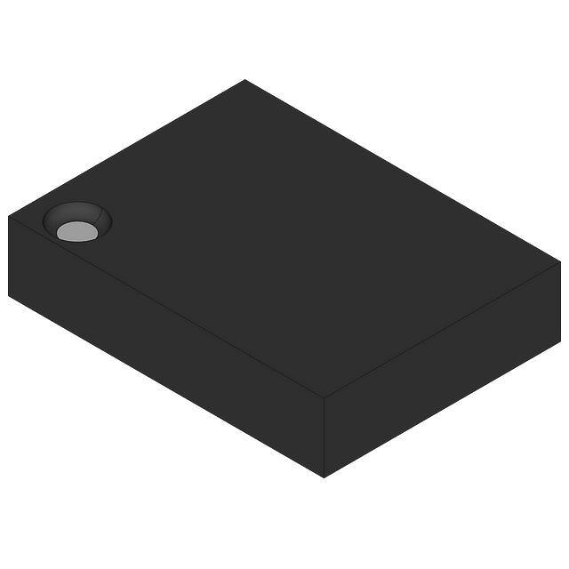
OUTLINE
The RP115x is a CMOS-based positive voltage regulator featuring 500 mA/ 1.0 A that provides high ripple
rejection, low dropout voltage, high output voltage accuracy, and low supply current. Internally, it consists of a
voltage reference unit, an error amplifier, a resistor-net for output voltage setting, a current limit circuit, a
thermal shutdown circuit, and a reverse current protection circuit. The RP115x uses a CMOS process for
achieving low supply current, low On Resistance for low dropout voltage (Typ. 0.195 V (DFN1216-8, IOUT = 1.0
A, VSET = 1.2 V)) and CE function for long battery life. Excellent ripple rejection, input transient response, and
load transient response make the RP115x ideal for the power sources of mobile communication equipment.
The RP115x is available in the DFN1216-8 package for space saving and the SOT-89-5 (Output Current: 1.0
A fixed) package for higher power applications. The RP115L (DFN1216-8) can choose the output current limit
between 1.0 A or 500 mA by alternating the LCON pin between “H” or “L”. The RP115H (SOT-89-5) can output
only 1.0 A since it does not include the LCON pin.
FEATURES
• Supply Current ·········································· Typ. 110 μA
• Supply Current (Standby Mode) ···················· Typ. 0.5 μA
• Dropout Voltage ········································· Typ. 0.195 V (DFN1216-8: IOUT = 1.0 A, VSET = 1.2 V)
•
•
•
•
•
•
•
•
•
•
•
•
•
(1)
Typ. 0.235 V (SOT-89-5: IOUT = 1.0 A, VSET = 1.2 V)
Ripple Rejection ········································· Typ. 80 dB (f = 1 kHz, VSET ≤ 1.8 V)
Typ. 75 dB (f = 1 kHz, VSET > 1.8 V)
Output Voltage Accuracy ······························ ±1.0% (VSET ≥ 1.75 V)
Output Voltage Temperature Coefficient ·········· Typ. ±30 ppm/ ºC (VSET ≥ 1.75 V)
Line Regulation ·········································· Typ. 0.02%/V
Package ··················································· DFN1216-8, SOT-89-5
Output Voltage Range ································· 0.7 V to 4.3 V with a 0.1-V step(1)
Built-in Short Current Limit Circuit ·················· Typ. 60 mA (DFN1216-8: LCON = "L")
Built-in Peak Current Limit
Built-in Thermal Shutdown Circuit ·················· Thermal Shutdown Temperature: 165ºC
Built-in Constant Slope Circuit for Start-up
Built-in Inrush Current Suppression Circuit ······· Typ. 300 mA (DFN1216-8: LCON = "L")
Reverse Current Protection
Recommended Ceramic Capacitors ··············· 1.0 µF or more
For the output voltage with a 0.05-V step, refer to SELECTION GUIDE.
1
�RP115x
NO. EA-274-170324
APPLICATIONS
• Portable Communication Equipment
• Electrical Appliances such as Cameras, VCRs and Camcorders
• Battery-powered Equipment
• Home Appliances, Printers, Scanners, Office Equipment Machines
SELECTION GUIDE
The package type, the set output voltage and the auto-discharge(1) are user-selectable options.
Selection Guide
Product Name
RP115Lxx1∗-E2
RP115Hxx1∗-T1-FE
Package
Quantity per Reel
Pb Free
Halogen Free
DFN1216-8
5,000 pcs
Yes
Yes
SOT-89-5
1,000 pcs
Yes
Yes
xx: Specify the set output voltage (VSET) within the range of 0.7 V to 4.3 V with a 0.1 V step.
Specify VSET with a 0.05 V step as follows:
0.75 V: RP115x071∗5
1.15 V: RP115x111∗5
1.25 V: RP115x121∗5
1.35 V: RP115x131∗5
1.75 V: RP115x171∗5
1.85 V: RP115x181∗5
2.15 V: RP115x211∗5
2.75 V: RP115x271∗5
2.85 V: RP115x281∗5
2.95 V: RP115x291∗5
∗: Specify the CE pin polarity and the auto-discharge.
B: CE = Active-high, auto-discharge not included
D: CE = Active-high, auto-discharge included
(1) Auto-discharge function quickly lowers the output voltage to 0 V by releasing the electrical charge in the external
capacitor when the chip enable signal is switched from the active mode to the standby mode.
2
�RP115x
NO. EA-274-170324
BLOCK DIAGRAMS
VDD
VOUT
-
Vref
VDD
VOUT
-
VFB
+
Current Limit
Thermal Shutdown
Current Limit
Thermal Shutdown
Reverce
Detector
GND
CE
Reverce
Detector
LCON
RP115Lxx1B Block Diagram
VDD
RP115Lxx1D Block Diagram
VOUT
-
+
VDD
CE
RP115Hxx1B(1) Block Diagram
(1) The
VOUT
-
VFB
+
Vref
VFB
Current Limit
Thermal Shutdown
Current Limit
Thermal Shutdown
Reverce
Detector
GND
CE
LCON
Vref
VFB
+
Vref
GND
Reverce
Detector
CE
GND
RP115Hxx1D Block Diagram
RP115H does not have the LCON pin, so the output current limit is fixed at 1 A.
3
�RP115x
NO. EA-274-170324
PIN DESCRIPTION
Bottom View
Top View
8
7
6
5
5
6
7
8
5
3
2
1
1
4
∗
1
2
3
4
4
DFN1216-8 Pin Configuration
2
3
SOT-89-5 Pin Configuration
RP115L: DFN1216-8
Pin No
Symbol
1
VOUT(1)
Pin Description
Output Pin
2
VOUT(1)
Output Pin
3
LCON
Output Current Limit Alternate Pin
4
VFB(1)
Feedback Pin
5
GND
Ground Pin
6
CE
7
VDD(2)
Input Pin
8
VDD(2)
Input Pin
Chip Enable Pin
* The tab on the bottom of the package shown by blue circle is a substrate potential (GND). It is recommended that this
tab be connected to the ground plane on the board but it is possible to leave the tab floating.
RP115H( 3): SOT-89-5
Pin No
Symbol
Pin Description
1
VFB(1)
Feedback Pin
2
GND
Ground Pin
3
CE
4
VDD
5
VOUT(1)
Chip Enable Pin
Input Pin
Output Pin
The VOUT pin and the VFB pin must be wired together when mounting on the board.
The VDD pins must be wired together when mounting on the board.
(3) The output current limit is fixed at 1 A.
(1)
(2)
4
�RP115x
NO. EA-274-170324
ABSOLUTE MAXIMUM RATINGS
Absolute Maximum Ratings
Symbol
Item
Rating
Unit
6.0
V
VIN
Input Voltage
VCE
Input Voltage (CE Pin)
−0.3 to 6.0
V
VLCON
Input Voltage (LCON Pin)
−0.3 to 6.0
V
VOUT
Output Voltage
−0.3 to 6.0
V
DFN1216-8
625
SOT-89-5
900
PD
Power Dissipation(1)
(Standard Land Pattern)
Tj
Junction Temperature Range
−40 to 125
°C
Tstg
Storage Temperature Range
−55 to 125
°C
mW
ABSOLUTE MAXIMUM RATINGS
Electronic and mechanical stress momentarily exceeded absolute maximum ratings may cause the permanent
damages and may degrade the life time and safety for both device and system using the device in the field. The
functional operation at or over these absolute maximum ratings is not assured.
RECOMMENDED OPERATING CONDITIONS
Recommended Operating Conditions
Symbol
Item
Voltage(2)
VIN
Input
Ta
Operating Temperature Range
Rating
Unit
1.4 to 5.25
V
−40 to 85
°C
RECOMMENDED OPERATING CONDITIONS
All of electronic equipment should be designed that the mounted semiconductor devices operate within the
recommended operating conditions. The semiconductor devices cannot operate normally over the recommended
operating conditions, even if when they are used over such conditions by momentary electronic noise or surge. And
the semiconductor devices may receive serious damage when they continue to operate over the recommended
operating conditions.
(1) Refer
(2)
to POWER DISSIPATION for detailed information.
In case of operating the device beyond 5.25 V, do not exceed 5.5 V with 500 total operating hours.
5
�RP115x
NO. EA-274-170324
ELECTRICAL CHARACTERISTICS
VIN = VSET(1) + 1.0 V, IOUT = 1 mA, CIN = COUT = 1.0 μF, unless otherwise noted.
The specifications surrounded by
are guaranteed by design engineering at −40ºC ≤ Ta ≤ 85ºC.
RP115x Electrical Characteristics
Symbol
Item
Conditions
Ta = 25°C
VOUT
Output Current Limit
∆VOUT
/∆IOUT
Load Regulation
VDIF
Dropout Voltage
ISS
VIN = VSET + 0.5 V
Typ.
(Ta = 25°C)
Max. Unit
VSET ≥ 1.75 V
x0.99
x1.01
V
VSET < 1.75 V
-18
+18
mV
x1.015
V
VSET ≥ 1.75 V
Output Voltage
−40°C ≤ Ta ≤ 85°C
ILIM
Min.
x0.985
VSET < 1.75 V
Refer to Set Output Voltagespecific Output Voltage
Characteristics.
LCON = ”L”
500
mA
1.0
A
LCON =
”H”(2)
VIN = VSET + 0.5 V
1 mA ≤ IOUT ≤ 500 mA
LCON = ”L”
VIN = VSET + 0.5 V
1 mA ≤ IOUT ≤ 1.0 A
LCON = ”H”(2)
1
20
40
mV
Refer to Set Output Voltage-specific Dropout Voltage Characteristics.
Supply Current
IOUT = 0 mA
110
160
μA
Istandby
Standby Current
VCE = 0 V
0.5
3.0
μA
∆VOUT
/∆VIN
Line Regulation
VSET + 0.5 V ≤ VIN ≤ 5.25 V
(VIN ≥ 1.4 V)
0.02
0.10
%/V
Ripple Rejection
f = 1 kHz,
Ripple 0.2 Vp-p,
VIN = VSET + 1.0 V,
IOUT = 30 mA
Output Voltage
Temperature Coefficient
−40°C ≤ Ta ≤ 85°C
ISC
Short Current Limit
VOUT = 0 V(3)
ICE
CE Pull-down Current
0.05
VCEH
CE Input Voltage “H”
1.0
VCEL
CE Input Voltage “L”
ILCON
LCON Pull-down Current
(RP115L only)
RR
∆VOUT
/∆Ta
VSET > 1.8 V
75
dB
VSET ≤ 1.8 V
80
dB
VSET ≥ 1.75 V
±30
VSET < 1.75 V
±100
ppm
/ºC
LCON = ”L”
LCON =
60
”H”(2)
mA
110
0.05
0.3
0.6
μA
V
0.3
0.4
V
0.6
µA
VSET: Set Output Voltage
The electrical characteristics of the RP115H is as same as when LCON = ”H”.
(3) The short current limit is the value when the VOUT pin is short circuited to GND after the device is completely started
up. The inrush current flows when the VOUT pin is short circuited to GND while the VOUT pin is short-circuited to GND
before the device is completely started up.
(1)
(2)
6
�RP115x
NO. EA-274-170324
ELECTRICAL CHARACTERISTICS (continued)
VIN = VSET(1) + 1.0 V, IOUT = 1 mA, CIN = COUT = 1.0 μF, unless otherwise noted.
The specifications surrounded by
are guaranteed by design engineering at -40ºC ≤ Ta ≤ 85ºC.
RP115x Electrical Characteristics
Symbol
Item
VLCONH
LCON Input Voltage “H”
(RP115L only)
VLCONL
LCON Input Voltage “L”
(RP115L only)
TTSD
TTSR
IREV
VREV_DET( 2)
VREV_REL( 4)
Thermal Shutdown
Temeprature Threshold
Reverse Current
Detection Offset Voltage in
Reverse Current Protection
Mode( 3)
Release Offset Voltage in
Reverse Current Protection
Mode(3)
Conditions
Typ.
(Ta = 25ºC)
Max.
Unit
1.0
V
0.4
V
Tj, Rising
165
ºC
Tj, Falling
110
ºC
VOUT = VSET + 1.0 V
0 ≤ VIN ≤ VOUT
VSET ≥ 1.75 V
VSET < 1.75 V
7.5
20
VOUT ≥ 0.7 V, 0 ≤ VIN ≤ 5.25 V
30
BW = 10 Hz to 100 kHz
RLOW
Auto-discharge Nch Tr. Onresistance
(RP115xx1D only)
VIN = 4.0 V, VCE = 0 V
IRUSH
Inrush Current Limit
CC mode(5)
VSET ≥ 1.75 V
VSET < 1.75 V
LCON = ”L”
LCON = ”H”(6)
µA
10
VOUT ≥ 0.7 V, 0 ≤ VIN ≤ 5.25 V
Output Noise
en
Min.
mV
50
mV
17
x VSET
35
x VSET
µVrms
60
Ω
300
mA
500
All test items listed under Electrical Characteristics are done under the pulse load condition (Tj ≈ Ta = 25ºC) except Output
Noise, Ripple Rejection, and Output Voltage Temperature Coefficient.
VSET: Set Output Voltage
VREV_DET = VIN − VOUT
(3) The guaranteed operating voltage range of the reverse current protection circuit is V
OUT ≥ 0.7 V. When VIN = VOUT = 0 V,
the reverse current protection mode is constantly active.
(4) V
REV_REL = VIN − VOUT
(5) For detailed information, refer to Start-up Characteristics Using Constant Slope Circuit.
(6) The electrical characteristics of the RP115H is as same as when LCON = ”H”.
(1)
(2)
7
�RP115x
NO. EA-274-170324
Set Output Voltage-specific Output Voltage Characteristics
Set Output Voltage
VSET (V)
Output Voltage
VOUT (mV)
Min.
Max.
0.7
−33
+28
0.8
−35
+29
0.9
−37
+30
1.0
−39
+31
1.1
−41
+33
1.2
−43
+34
1.3
−45
+35
1.4
−47
+36
1.5
−49
+38
1.6
−51
+39
1.7
−53
+40
Set Output Voltage-specific Dropout Voltage Characteristics
RP115L: DFN1216-8
(Ta = 25°C)
Dropout Voltage VDIF (V)
Set Output Voltage
VSET (V)
RP115L
IOUT = 500 mA
RP115H
IOUT = 1000 mA
IOUT = 1000 mA
Typ.
Max.
Typ.
Max.
Typ.
Max.
0.7 ≤ VSET < 1.1
*
*
*
*
*
*
1.1 ≤ VSET < 1.2
*
*
*
0.300
*
0.350
1.2 ≤ VSET < 1.3
*
*
0.195
0.275
0.235
0.330
1.3 ≤ VSET < 1.5
0.095
0.135
0.185
0.260
0.225
0.320
1.5 ≤ VSET < 1.75
0.085
0.120
0.165
0.235
0.205
0.295
1.75 ≤ VSET < 2.6
0.075
0.110
0.150
0.215
0.190
0.270
2.6 ≤ VSET < 3.3
0.065
0.090
0.130
0.180
0.170
0.240
3.3 ≤ VSET ≤ 4.3
0.060
0.085
0.125
0.170
0.165
0.225
If the dropout voltage falls below the release offset value of reverse current protection mode (VREV_REL), the reverse current
protection circuit may repeat the detection and release operations. Please refer to Reverse Current Protection Circuit.
* Input voltage should be equal or more than the minimum operating voltage (1.4 V).
8
�RP115x
NO. EA-274-170324
THEORY OF OPERATION
Reverse Current Protection Circuit
The RP115x includes a Reverse Current Protection Circuit, which stops the reverse current from VOUT pin to
VDD pin or to GND pin when VOUT becomes higher than VIN. Usually, the LDO using Pch output transistor
contains a parasitic diode between VDD pin and VOUT pin. Therefore, if VOUT is higher than VIN, the parasitic
diode becomes forward direction. As a result, the current flows from VOUT pin to VDD pin. The RP115x switches
the mode to the reverse current protection mode before VIN becomes lower than VOUT by connecting the
parasitic diode of Pch output transistor to the backward direction, and connecting the gate to VOUT pin. As a
result, the Pch output transistor is turned off. However, from VOUT pin to GND pin, via the internal divider
resistors, very small current IREV flows.
Switching to either the normal mode or to the reverse current protection mode is determined by the magnitude
of VIN voltage and VOUT voltage. For the stable operation, offset and hysteresis are set as the threshold. The
detector threshold is set to VREV_DET and the released voltage is set to VREV_REL. Therefore, the minimum
dropout voltage under the small load current condition is restricted by the value of VREV_REL.
Following figures show the diagrams of each mode, and the load characteristics of each mode. When giving
the VOUT pin a constant-voltage and decreasing the VIN voltage, the dropout voltage will become lower than
VREV_DET. As a result, the reverse current protection starts to function to stop the load current. By increasing
the dropout voltage higher than VREV_REL, the protection mode will be released to let the load current to flow. If
the dropout voltage to be used is lower than VREV_REL, the detection and the release may be repeated. The
operating voltage guaranteed level of the reverse current protection circuit is for VOUT ≥ 0.7V. If VIN=0V, the
reverse current protection mode becomes always active.
VDD
Reverse
Detector
VDD
Reverse
Detector
IOUT
VOUT
VOUT
+
+
Vref
Vref
CE
GND
Normal Operation Mode
IREV
GND
CE
Reverse Current Protection Mode
9
�RP115x
Output/ Reverse Current
IOUT/ IREV
Input/ Output Voltage
VIN/ VOUT [V]
NO. EA-274-170324
VIN
VREV_REL
VREV_DET
VOUT
IOUT
Normal Mode
Reverse Current Protection Mode
Normal
Mode
0
IREV
Detection/ Release Timing of Reverse Current Protection
Start-up Characteristics Using Constant Slope Circuit
Constant slope circuit is included in the RP115x to prevent the overshoot of the output voltage. The start-up
time (tON) is 100 µs (Typ.). If inrush current increases due to the large capacitance of COUT, the operation mode
will be shifted from Constant Slope (CS) mode to Constant Current (CC) mode. The CC mode maintains a
constant level of inrush current. In the CC mode, tON varies according to the size of COUT and the amount of
load current.
Start-up Time and Inrush Current Estimations
Start-up time and inrush current in the CS mode and the CC mode can be estimated as follows.
[CS Mode]
Start-up Time: tON = 100 μs (Typ.)
Inrush Current: IRUSH = COUT ∙ VSET / tON + IOUT(1)
Note: If the result of the above calculation is more than the following values, the operation mode will be
shifted from the CS mode to the CC mode.
LCON = ”L” ········································································· 300 mA (Typ.)
LCON = ”H” ········································································· 500 mA (Typ.)
[CC Mode]
Start-up Time: tON = COUT ∙ VSET / ICO(2)
Inrush Current: IRUSH
LCON = ”L” ·········································································· 300 mA (Typ.)
LCON = ”H” ·········································································· 500 mA (Typ.)
(1)
(2)
IOUT: When RLOAD is connected to load, IOUT can be calculated by RLOAD = VSET / IOUT.
ICO: ICO is a charge current of COUT and can be calculated roughly by IRUSH ≈ ICO + IOUT.
10
�RP115x
NO. EA-274-170324
IRUSH
VDD VOUT
VIN
CIN
LCON Control
CE Control
RP115L
LCON VFB
ICO*20
IOUT*19
COUT RLOAD
CE
GND
Circuit Example
VIN
VIN ≥1.4V
CE
CS Mode
VOUT
tON = 100µs (Typ.)
VSET
60µs (Typ.)
IOUT ≤ 500mA (LCON=”L”)
≤ 1.0A (LCON=”H”)
IRUSH = COUT • VSET / tON + IOUT
IOUT
IRUSH
CC Mode
VOUT
tON = COUT • VSET / ICO
VSET
60µs (Typ.)
IOUT ≤ 150mA (LCON=”L”)
≤ 350mA (LCON=”H”)
IRUSH
IOUT ≤ 500mA (LCON=”L”)
≤ 1.0A (LCON=”H”)
IRUSH = 300mA (LCON=”L”)
500mA (LCON=”H”)
IOUT
Timing Chart of Start-up Operation
11
�RP115x
NO. EA-274-170324
Precautions before Use
During the start-up, the inrush current limit circuit is in operation; therefore, the load current (IOUT) should be
drawn after the output voltage (VOUT) reached the preset value (Best timing: tON + 60 µs or more). If the load
current is drawn during the start-up, it should be within the following values.
LCON = ”L” ··························································· IOUT ≤ 150 mA
LCON = ”H” ··························································· IOUT ≤ 350 mA
In the CC mode, IRUSH is limited until VOUT reaches the preset value. IRUSH ≈ ICO + IOUT is true; therefore, if large
IOUT is drawn during the start-up, the charge current (ICO) of COUT decreases and tON becomes longer. Please
refer to Start-up Time and Inrush Current Estimations.
In order to control the start-up operation by using the CS mode or CC mode, input “H” into the CE pin while
VIN ≥ 1.4 V. If “H” is input into the CE pin while VIN is less than the minimum operating voltage, the operation
may not be controlled by the CS mode or CC mode.
When starting up the device while the short circuit is occurring between the VOUT pin and GND, the short current
protection circuit does not control the current but the current limit circuit does.
When there’s excessive heat generation in the device, thermal shutdown circuit shuts down the circuitry before
the device overheats dangerously.
LCON Pin (RP115L only)
By alternating the LCON pin between “H” or “L”, the RP115L can choose the output current limit either 1.0 A
or 500 mA. Please note that during start-up (tON + 60 µs (Typ.)), do not change the logic of the LCON pin.
LCON = ”L” ·········································· 500 mA
LCON = ”H” ·········································· 1.0 A
Application Example
Even when using the RP115L with LCON = ”H”, IRUSH in the CC mode can be reduced from 500 mA (Typ.) to
300 mA (Typ.) by starting up the IC with LCON = ”L”. Please refer to Start-up Characteristics Using Constant
Slope Circuit.
12
�RP115x
NO. EA-274-170324
APPLICATION INFORMATION
VDD
VIN
VOUT
VOUT(2)
RP115x
CIN
LCON(1) VFB(2)
COUT
LCON Control
CE
CE Control
GND
RP115x Typical Application Circuit
1
External Components
Symbol
Description
CIN
1.0 μF, Ceramic Capacitor, GRM155R61A105KE15 (MURATA)
1.0 µF, Ceramic Capacitor, GRM155R61A105KE15 (MURATA)
COUT
2.2 µF, Ceramic Capacitor, GRM155R61A225KE95 (MURATA)
Precautions When Selecting External Components
•
In this device, phase compensation is provided to secure stable operation even when the load current is
varied. For this purpose, use a 1.0-µF or more output capacitor (COUT).
•
A ceramic capacitor has different temperature characteristics and bias dependencies depending on the
size, manufacturer or part number of a capacitor. Careful evaluation is required. When using a 1.75-V
product under the environment of −20°C or lower, choose a 2.2-µF or more COUT.
•
In case of using a tantalum-type capacitor with a large ESR (Equivalent Series Resistance), the output
might become unstable. Careful evaluation on frequency characteristics is required.
(1)
(2)
The LCON pin is included in the RP115L (DFN2020-8B) only.
Connect the VOUT and VFB pins together.
13
�RP115x
NO. EA-274-170324
Equivalent Series Resistance (ESR) vs. Output Current
Ceramic type output capacitor is recommended for the RP115x but any capacitor with low ESR can be used.
The graphs below show the relation between IOUT and ESR (noise level: average 40 μV or less).
Measurement Conditions
Noise Frequency Band Width: 10 Hz to 2 MHz
Operating Temperature Range: −40°C to +85°C
Hatched Area: Output noise level is average 40μV or less.
CIN, COUT: 1.0 μF or more
RP115x071x
100
V IN = 4.3V to 5.25V
100
Ta = -40°C to 85°C
Ta = -40°C to 85°C
10
ESR [Ω]
10
ESR [Ω]
RP115x431x
V IN = 1.4V to 5.25V
1
0.1
1
0.1
0.01
0.01
0
200
400
600
800
Output Current IOUT [mA]
1000
0
200
400
600
800
Output Current IOUT [mA]
1000
TECHNICAL NOTES
The performance of a power source circuit using this device is highly dependent on a peripheral circuit. A
peripheral component or the device mounted on PCB should not exceed its rated voltage, rated current or
rated power. When designing a peripheral circuit, please be fully aware of the following points.
Place the external components as close as possible to the device with shortest-distance wirings. Connect
an input capacitor (CIN) between the VIN and GND pins with shortest-distance wiring.
Ensure the VDD and GND wirings are sufficiently robust. If the impedance of wiring between the VDD
and GND pins is high, it may cause noise pickup or unstable operation.
14
Connect an output capacitor (COUT) between the VOUT and GND pins with shortest-distance wiring.
�RP115x
NO. EA-274-170324
TYPICAL CHARACTERISTICS
Note: Typical Characteristics are intended to be used as reference data; they are not guaranteed.
1) Output Voltage vs. Input Voltage (CIN = Ceramic 1.0 μF, COUT = Ceramic 1.0 μF, Ta = 25°C)
RP115x171x
1
0.9
0.8
0.7
0.6
0.5
0.4
0.3
0.2
0.1
0
Output Voltage V OUT[V]
Output Voltage V OUT[V]
RP115x071x
Iout = 1mA
Iout = 30mA
Iout = 50mA
0
1
2
3
4
2
1.8
1.6
1.4
1.2
1
0.8
0.6
0.4
0.2
0
5
Iout = 1mA
Iout = 30mA
Iout = 50mA
0
1
Input Voltage V IN[V]
1
2
3
Output Voltage V OUT[V]
Output Voltage V OUT[V]
4
5
RP115x431x
Iout = 1mA
Iout = 30mA
Iout = 50mA
0
3
Input Voltage V IN[V]
RP115x181x
2
1.8
1.6
1.4
1.2
1
0.8
0.6
0.4
0.2
0
2
4
Input Voltage V IN[V]
5
5
4.5
4
3.5
3
2.5
2
1.5
1
0.5
0
Iout = 1mA
Iout = 30mA
Iout = 50mA
0
1
2
3
4
5
Input Voltage V IN[V]
15
�RP115x
NO. EA-274-170324
2) Supply Current vs. Input Voltage (CIN = Ceramic 1.0 μF, COUT = Ceramic 1.0 μF, Ta = 25°C)
RP115x171x
140
140
120
120
Supply Current ISS[μA]
Supply Current ISS[μA]
RP115x071x
100
80
60
40
20
0
100
80
60
40
20
0
0
1
2
3
4
5
0
1
Input Voltage V IN[V]
3
4
5
4
5
Input Voltage V IN[V]
RP115x181x
RP115x431x
140
140
120
120
Supply Current ISS[μA]
Supply Current ISS[μA]
2
100
80
60
40
20
0
100
80
60
40
20
0
0
1
2
3
Input Voltage V IN[V]
4
5
0
1
2
3
Input Voltage V IN[V]
Short Current Limit vs. Temperature and Current Limit vs. Temperature
The RP115x contains a peak current limit circuit which protect the regulator from damage by overcurrent if the
output pin (VOUT) and the ground pin (GND) are shorted. The short-circuiting causes the overheating of the
device which leads a thermal shutdown circuit to operate. If the peak current limit circuit and the thermal
shutdown circuit work at the same time, fold-back type dropping characteristics cannot be measured. As for
the short-circuit current and the peak current limit circuit, please refer to 3) Short Current Limit vs. Temperature
and 4) Current Limit vs. Temperature.
16
�RP115x
NO. EA-274-170324
3) Short Current Limit vs. Temperature
V IN = 2.0V
V OUT = 0V
LCON = "L"
RP115x071x
120
Short Current Limit [mA]
Short Current Limit [mA]
70
65
60
55
V IN = 2.0V
V OUT = 0V
LCON = "H"
RP115x071x
50
115
110
105
100
95
90
-40 -25
0
25
50
Temperature Ta [°C]
75 85
-40 -25
0
25
50
Temperature Ta [°C]
75 85
4) Peak Current Limit vs. Temperature
V IN = 1.2V
LCON = "L"
900
1500
850
1450
800
750
700
650
600
-40 -25
0
25
50
Temperature Ta [°C]
75 85
V IN = 1.2V
LCON = "H"
RP115x071x
Current Limit [mA]
Current Limit [mA]
RP115x071x
1400
1350
1300
1250
1200
-40 -25
0
25
50
75 85
Temperature Ta [°C]
17
�RP115x
NO. EA-274-170324
5) Output Voltage vs. Temperature (CIN = Ceramic 1.0 μF, COUT = Ceramic 1.0 μF, IOUT = 1 mA)
RP115x071x
0.74
RP115x171x
V IN = 1.7V
1.74
1.73
Output Voltage VOUT[V]
Output Voltage VOUT[V]
0.73
0.72
0.71
0.7
0.69
0.68
0.67
0.66
0
25
50
Temperature Ta [°C]
RP115x181x
1.84
1.71
1.7
1.69
1.68
1.67
75 85
-40 -25
0
25
50
Temperature Ta [°C]
RP115x431x
V IN = 2.8V
4.34
75 85
V IN = 5.25V
4.33
Output Voltage VOUT[V]
1.83
Output Voltage VOUT[V]
1.72
1.66
-40 -25
1.82
1.81
1.8
1.79
1.78
1.77
1.76
4.32
4.31
4.3
4.29
4.28
4.27
4.26
-40 -25
18
V IN = 2.7V
0
25
50
Temperature Ta [°C]
75 85
-40 -25
0
25
50
Temperature Ta [°C]
75 85
�RP115x
NO. EA-274-170324
6) Supply Current vs. Temperature (CIN = Ceramic 1.0 μF, COUT = Ceramic 1.0 μF, IOUT = 0 mA)
RP115x071x
120
110
100
90
80
70
120
110
100
90
80
70
-40 -25
0
25
50
Temperature Ta [°C]
RP115x181x
130
75 85
-40 -25
120
110
100
90
80
0
25
50
Temperature Ta [°C]
RP115x431x
V IN = 2.8V
130
Supply Current ISS[μA]
Supply Current ISS[μA]
V IN = 2.7V
130
Supply Current ISS[μA]
Supply Current ISS[μA]
130
RP115x171x
V IN = 1.7V
75 85
V IN = 5.25V
120
110
100
90
80
70
70
-40 -25
0
25
50
Temperature Ta [°C]
75 85
-40 -25
0
25
50
Temperature Ta [°C]
75 85
19
�RP115x
NO. EA-274-170324
7) Dropout Voltage vs. Output Current (CIN = Ceramic 1.0 μF, COUT = Ceramic 1.0 μF)
RP115L171x
RP115H171x
250
Dropout Voltage VDIF [mV]
Dropout Voltage VDIF [mV]
250
-40°C
25°C
85°C
200
150
100
50
0
200
400
600
800
50
0
600
800
RP115L181x
RP115H181x
-40°C
25°C
85°C
150
400
Output Current IOUT [mA]
250
200
200
Output Current IOUT [mA]
Dropout Voltage VDIF [mV]
Dropout Voltage VDIF [mV]
100
1000
250
100
50
0
1000
-40°C
25°C
85°C
200
150
100
50
0
0
250
200
400
600
800
1000
200
400
600
800
Output Current IOUT [mA]
RP115L431x
RP115H431x
250
-40°C
25°C
85°C
200
0
Output Current IOUT [mA]
Dropout Voltage VDIF [mV]
Dropout Voltage VDIF [mV]
150
0
0
150
100
50
1000
-40°C
25°C
85°C
200
150
100
50
0
0
0
200
400
600
800
Output Current IOUT [mA]
20
-40°C
25°C
85°C
200
1000
0
200
400
600
800
Output Current IOUT [mA]
1000
�RP115x
NO. EA-274-170324
8) Dropout Voltage vs. Set Output Voltage (CIN = Ceramic 1.0 μF, COUT = Ceramic 1.0 μF, Ta = 25°C)
9) Dropout Voltage vs. Temperature (CIN = Ceramic 1.0 μF, COUT = Ceramic 1.0 μF)
400
300
200
100
0
-40 -25
0
25
50
Temperature Ta [°C]
RP115L181x
Dropout Voltage VDIF [mV]
300
250
30mA
100mA
300mA
500mA
1000mA
150
100
50
0
0
25
50
Temperature Ta [°C]
300
250
75 85
30mA
100mA
300mA
500mA
1000mA
200
150
100
50
0
-40 -25
75 85
200
-40 -25
RP115L171x
Dropout Voltage VDIF [mV]
Dropout Voltage VDIF [mV]
500
30mA
100mA
300mA
500mA
1000mA
0
25
50
Temperature Ta [°C]
RP115L431x
300
Dropout Voltage VDIF [mV]
RP115L071x
250
75 85
30mA
100mA
300mA
500mA
1000mA
200
150
100
50
0
-40 -25
0
25
50
Temperature Ta [°C]
75 85
21
�RP115x
NO. EA-274-170324
400
300
200
100
0
-40 -25
0
25
50
Temperature Ta [°C]
200
150
100
50
0
-40 -25
0
25
50
75 85
Temperature Ta [°C]
30mA
100mA
300mA
500mA
1000mA
300
Dropout Voltage VDIF [mV]
250
75 85
RP115H181x
250
200
150
100
50
0
-40 -25
300
0
25
50
Temperature Ta [°C]
30mA
100mA
300mA
500mA
1000mA
RP115H431x
300
Dropout Voltage VDIF [mV]
Dropout Voltage VDIF [mV]
500
30mA
100mA
300mA
500mA
1000mA
RP115H171x
Dropout Voltage VDIF [mV]
30mA
100mA
300mA
500mA
1000mA
RP115H071x
250
200
150
100
75 85
50
0
-40 -25
0
25
50
Temperature Ta [°C]
75 85
10) Ripple Rejection vs. Input Voltage (CIN = none, COUT = Ceramic 1.0 μF, Ripple = 0.2 Vp-p, Ta = 25°C)
100
90
80
70
60
50
40
30
20
10
0
0.1kHz
1kHz
10kHz
100kHz
0
1
2
3
4
Input Voltage VIN(V)
22
RP115x071x
IOUT=1mA
Ripple Rejection RR(dB)
Ripple Rejection RR(dB)
RP115x071x
5
100
90
80
70
60
50
40
30
20
10
0
IOUT=30mA
0.1kHz
1kHz
10kHz
100kHz
0
1
2
3
Input Voltage VIN(V)
4
5
�RP115x
RP115x171x
0.1kHz
1kHz
10kHz
100kHz
20
10
0
1
Ripple Rejection RR(dB)
IOUT=1mA
2
3
4
Input Voltage VIN(V)
RP115x181x
100
90
80
70
60
50
40
30
20
10
0
2
3
0.1kHz
1kHz
10kHz
100kHz
10
0
2
5
4.2
4.4
4.6
4.8
Input Voltage VIN(V)
IOUT=30mA
2
3
4
5
Input Voltage VIN(V)
IOUT=1mA
0.1kHz
1kHz
10kHz
100kHz
4
5
0.1kHz
1kHz
10kHz
100kHz
1
5
5.2
Ripple Rejection RR(dB)
Ripple Rejection RR(dB)
RP115x431x
3
4
Input Voltage VIN(V)
RP115x181x
100
90
80
70
60
50
40
30
20
10
0
Input Voltage VIN(V)
100
90
80
70
60
50
40
30
20
10
0
IOUT=30mA
60
50
40
30
20
1
IOUT=1mA
4
RP115x171x
100
90
80
70
5
0.1kHz
1kHz
10kHz
100kHz
1
Ripple Rejection RR(dB)
100
90
80
70
60
50
40
30
Ripple Rejection RR(dB)
Ripple Rejection RR(dB)
NO. EA-274-170324
RP115x431x
100
90
80
70
60
50
40
30
20
10
0
IOUT=30mA
0.1kHz
1kHz
10kHz
100kHz
4
4.2
4.4
4.6
4.8
5
5.2
Input Voltage VIN(V)
23
�RP115x
NO. EA-274-170324
11) Ripple Rejection vs. Frequency (CIN = none, COUT = Ceramic 1.0 μF, Ripple = 0.2 Vp-p, Ta = 25°C)
RP115x071x
100
80
60
40
1mA
30mA
150mA
20
0
0.1
1
100
80
60
40
1mA
30mA
150mA
20
0
10
100
1000
0.1
1
Frequency f [kHz]
80
60
1mA
30mA
150mA
20
0
0.1
1
100
1000
1000
VIN = 5.25V
120
100
80
60
40
1mA
30mA
150mA
20
0
10
100
RP115x431x
VIN = 2.8V
100
40
10
Frequency f [kHz]
Ripple Rejection RR [dB]
Ripple Rejection RR [dB]
RP115x181x
120
VIN = 2.7V
120
Ripple Rejection RR [dB]
Ripple Rejection RR [dB]
RP115x171x
VIN = 1.7V
120
0.1
Frequency f [kHz]
1
10
100
1000
Frequency f [kHz]
Output Voltage
-20 -10 0 10 20 30 40 50 60 70 80
Time t [μs]
24
Input Voltage
2.7V 3.7V
1.73
1.72
1.71
1.7
1.69
Output Voltage
-20 -10 0
10 20 30 40 50 60 70 80
Time t [μs]
5
4
3
2
1
0
Input Voltage VIN [V]
0.73
0.72
0.71
0.7
0.69
0.68
Input Voltage
1.7V 2.7V
5
4
3
2
1
0
RP115x171x
Output Voltage VOUT [V]
Output Voltage V OUT [V]
RP115x071x
Input Voltage VIN [V]
12) Line Transient Response CIN = none, COUT = Ceramic 1.0 μF, IOUT = 30 mA, tr = tf = 5 μs, Ta = 25°C)
�RP115x
NO. EA-274-170324
5
4
3
2
1
0
Output Voltage VOUT [V]
Input Voltage
2.8V 3.8V
1.82
1.81
1.8
1.79
1.78
Input Voltage VIN [V]
RP115x181x
Output Voltage
-20 -10 0 10 20 30 40 50 60 70 80
Time t [μs]
VIN = 1.7V
Output Voltage VOUT [V]
50
Load Current
50mA 100mA
0.71
0
0.7
0.69
Output Voltage
0.68
-5 0
5 10 15 20 25 30 35 40
Output Voltage VOUT [V]
100
Load Current
1mA 250mA
0.8
0.75
0.7
0.65
0.6
0.55
Output Voltage
-20
0
0.8
0.75
0.7
0.65
0.6
0.55
VIN = 1.7V
600
400
200
0
Output Voltage
-20
0
20 40 60 80 100 120 140
Time t [μs]
RP115x171x
Output Voltage VOUT [V]
Output Voltage VOUT [V]
Load Current
1mA 500mA
20 40 60 80 100 120 140
Time t [μs]
Output Current I OUT [mA]
Time t [μs]
RP115x071x
300
200
100
0
Output Current I OUT [mA]
RP115x071x
VIN = 1.7V 150
VIN = 2.7V
Load Current
50mA 100mA
1.72
1.71
1.7
1.69
1.68
1.67
150
100
50
0
Output Current I OUT [mA]
RP115x071x
Output Current I OUT [mA]
13) Load Transient Response (CIN = Ceramic 1.0 μF, COUT = Ceramic 1.0 μF, tr = tf = 0.5 μs, Ta = 25°C)
Output Voltage
-5 0
5 10 15 20 25 30 35 40
Time t [μs]
25
�RP115x
Output Voltage
-20
0
20 40 60 80 100 120 140
Load Current
1mA 500mA
1.8
1.75
1.7
1.65
1.6
1.55
Output Voltage
-20
0
20 40 60 80 100 120 140
Time t [μs]
Load Current
50mA 100mA
1.81
1.8
1.79
1.78
1.77
1.76
150
100
50
0
Output Voltage
-5 0
5 10 15 20 25 30 35 40
RP115x181x
VIN = 2.8V
Output Voltage V OUT [V]
Output Voltage V OUT [V]
VIN = 2.8V
Output Current I OUT [mA]
Time t [μs]
RP115x181x
Load Current
1mA 250mA
1.85
1.8
1.75
1.7
1.65
-20
0
20 40 60 80 100 120 140
time [μs]
600
400
200
0
RP115x431x
Output Voltage V OUT [V]
0
Output Current I OUT [mA]
Output Voltage V OUT [V]
26
VIN = 2.8V
Output Voltage
-20
20 40 60 80 100 120 140
time [μs]
Load Current
1mA 500mA
1.85
1.8
1.75
1.7
1.65
300
200
100
0
Output Voltage
time [μs]
RP115x181x
600
400
200
0
Output Current I OUT [mA]
1.8
1.75
1.7
1.65
1.6
1.55
VIN = 2.7V
Output Current I OUT [mA]
Load Current
1mA 250mA
300
200
100
0
VIN = 5.25V
Load Current
50mA 100mA
4.32
4.31
4.3
4.29
4.28
Output Voltage
-5 0
5 10 15 20 25 30 35 40
time [μs]
150
100
50
0
Output Current I OUT [mA]
Output Voltage VOUT [V]
VIN = 2.7V
RP115x171x
Output Voltage VOUT [V]
RP115x171x
Output Current I OUT [mA]
NO. EA-274-170324
�RP115x
Load Current
1mA 250mA
4.4
4.35
4.3
4.25
4.2
4.15
300
200
100
0
Output Voltage
-20 0
20 40 60 80 100 120 140
RP115x431x
VIN = 5.25V
Output Voltage V OUT [V]
Output Voltage V OUT [V]
VIN = 5.25V
Output Current I OUT [mA]
RP115x431x
600
400
200
0
Load Current
1mA 500mA
4.4
4.35
4.3
4.25
4.2
4.15
Output Current I OUT [mA]
NO. EA-274-170324
Output Voltage
-20 0
20 40 60 80 100 120 140
time [μs]
time [μs]
0
Iout = 0mA
Iout = 30mA
Iout = 150mA
1
0.5
1
Output Voltage
0
-20 0
50
100
150 180
Time t [μs]
VIN = 2.8V
Output Voltage VOUT [V]
4
2
CE Input Voltage
0V => 2.8V
2
0
Output Voltage
Iout = 0mA
Iout = 30mA
Iout = 150mA
1
0
-20 0
50
100
Time t [μs]
4
CE Input Voltage
0V => 2.7V
2
0
2
1
Output Voltage
Iout = 0mA
Iout = 30mA
Iout = 150mA
0
-20 0
50
100
150 180
Time t [μs]
150 180
CE Input Voltage VCE[V]
RP115x181x
VIN = 2.7V
RP115x431x
VIN = 5.25V
4
CE Input Voltage
0V => 5.25V
4
8
0
CE Input Voltage VCE[V]
Output Voltage VOUT [V]
CE Input Voltage
0V => 1.7V
RP115x071x
CE Input Voltage VCE [V]
2
Output Voltage VOUT [V]
VIN = 1.7V
Output Voltage VOUT [V]
RP115x071x
CE Input Voltage VCE [V]
14) Turn-on Waveform by CE Pin Signal (CIN = Ceramic 1.0 μF, COUT = Ceramic 1.0 μF, Ta = 25°C)
Output Voltage
Iout = 0mA
Iout = 30mA
Iout = 150mA
2
0
-20 0
50
100
Time t [μs]
150 180
27
�RP115x
NO. EA-274-170324
VIN = 1.7V
Output Voltage
0.5
Iout = 0mA
Iout = 30mA
Iout = 150mA
Iout = 0mA
Iout = 30mA
Iout = 150mA
100
200
300
Time t [μs]
400450
VIN = 2.8V
Iout = 0mA
Iout = 30mA
Iout = 150mA
0
200
300
Time t [μs]
400 450
CE Input Voltage
5.25V => 0V
2
Output Voltage
100
RP115x431D VIN = 5.25V
4
0
1
-50 0
8
4
0
Output Voltage
4
Iout = 0mA
Iout = 30mA
Iout = 150mA
2
0
-50 0
100
200
300
Time t [μs]
400 450
CE Input Voltage VCE[V]
Output Voltage VOUT [V]
2
0
-50 0
CE Input Voltage
2.8V => 0V
28
Output Voltage
1
0
RP115x181D
2
2
Output Voltage VOUT [V]
1
4
0
Output Voltage VOUT [V]
0
VIN = 2.7V
CE Input Voltage
2.7V => 0V
1
CE Input Voltage VCE[V]
Output Voltage VOUT [V]
CE Input Voltage
1.7V => 0V
RP115x171D
2
CE Input Voltage VCE[V]
RP115x071D
CE Input Voltage VCE[V]
15) Turn-off Waveform by CE Pin Signal (CIN = Ceramic 1.0 μF, COUT = Ceramic 1.0 μF, Ta = 25°C)
-50 0
100
200
300
Time t [μs]
400 450
�RP115x
NO. EA-274-170324
Cout = 1.0μF
Cout = 2.2μF
Cout = 4.7μF
Cout = 10μF
Inrush Current Irush [mA]
Output Voltage
400
300
200
Inrush Current 100
0
-50
0
50
100
Time t [μs]
150
200
RP115L181x (LCON="L", CS mode)
VIN = 2.8V
3
2.5
2
1.5
1
0.5
0
CE Input Voltage
0V => 2.8V
Cout = 1.0μF
Cout = 2.2μF
Cout = 4.7μF
Cout = 10μF
Inrush Current Irush [mA]
Output Voltage
400
300
200
Inrush Current
100
0
-50
0
50
100
Time t [μs]
150
200
3
2.5
2
1.5
1
0.5
0
0
50
100 150 200 250
Time t [μs]
Inrush Current Irush [mA]
[V] / CE Input Voltage V CE[V]
OUT
-50
RP115L171x (LCON="L", CC mode)
VIN = 2.7V
CE Input Voltage
0V => 2.7V
Output Voltage
Cout = 22μF
Inrush Current
-50
0
50
Inrush Current Irush [mA]
CE Input Voltage
0V => 2.7V
400
300
Inrush Current
200
100
0
400
300
200
100
0
100 150 200 250
Time t [μs]
RP115L181x (LCON="L", CC mode)
VIN = 2.8V
3
2.5
2
1.5
1
0.5
0
CE Input Voltage
0V => 2.8V
Output Voltage
Cout = 22μF
Inrush Current
-50
0
400
300
200
100
0
50 100 150 200 250
Time t [μs]
Inrush Current Irush [mA]
200
VIN = 2.7V
3
2.5
2
1.5
1
0.5
0
Output Voltage V
[V] / CE Input Voltage V CE[V]
150
RP115L171x (LCON="L", CS mode)
OUT
Output Voltage V
50
100
Time t [μs]
Output Voltage
Cout = 47μF
Output Voltage V
0
[V] / CE Input Voltage V CE[V]
-50
CE Input Voltage
0V => 1.7V
OUT
400
300
200
Inrush Current100
0
2
1.5
1
0.5
0
Output Voltage V
Cout = 1.0μF
Cout = 2.2μF
Cout = 4.7μF
Cout = 10μF
Cout = 22μF
Inrush Current Irush [mA]
Output Voltage
[V] / CE Input Voltage V CE[V]
CE Input Voltage
0V => 1.7V
RP115L071x (LCON="L", CC mode)
VIN = 1.7V
OUT
2
1.5
1
0.5
0
Output Voltage V
RP115L071x (LCON="L", CS mode)
VIN = 1.7V
OUT
[V] / CE Input Voltage V CE[V]
Output Voltage V OUT [V] / CE Input Voltage V CE[V]
16) Inrush Current (CIN = Ceramic 1.0 μF, IOUT = 0 mA, Ta = 25°C)
29
�RP115x
0
50
100
Time t [μs]
150
200
RP115x171x (LCON="H", CS mode)
VIN = 2.7V
3
2.5
2
1.5
1
0.5
0
CE Input Voltage
0V => 2.7V
Output Voltage
Cout = 1.0μF
Cout = 2.2μF
Cout = 4.7μF
Cout = 10μF
500
400
300
Inrush Current 200
100
0
-50
0
50
100
Time t [μs]
150
200
Output Voltage V
Inrush Current
-50
2
1.5
1
0.5
0
0
50 100 150
Time t [μs]
200
400
300
200
100
0
250
Inrush Current Irush [mA]
Cout = 10μF
OUT
[V] / CE Input Voltage V CE[V]
Output Voltage
RP115x071x (LCON="H", CC mode)
VIN = 1.7V
CE Input Voltage
0V => 1.7V
Output Voltage
Cout = 100μF
500
Inrush Current400
300
200
100
0
-50
0
50
100 150 200 250
Time t [μs]
Inrush Current Irush [mA]
-50
Inrush Current Irush [mA]
Output Voltage
Cout = 1.0μF
Cout = 2.2μF 500
Cout = 4.7μF
Cout = 10μF 400
Cout = 22μF
Cout = 47μF 300
200
Inrush Current100
0
CE Input Voltage
0V => 5.25V
RP115x171x (LCON="H", CC mode)
VIN = 2.7V
3
2.5
CE Input Voltage
2
0V => 2.7V
1.5
Output Voltage
1
0.5
0
Cout = 22μF 500
400
300
Inrush Current
200
100
0
-50
0
50
100 150 200 250
Time t [μs]
Inrush Current Irush [mA]
CE Input Voltage
0V => 1.7V
[V] / CE Input Voltage V CE[V]
2
1.5
1
0.5
0
RP115L431x (LCON="L", CC mode)
VIN = 5.25V
6
5
4
3
2
1
0
OUT
RP115x071x (LCON="H", CS mode)
VIN = 1.7V
Output Voltage V
200
Inrush Current Irush [mA]
Output Voltage V
30
150
[V] / CE Input Voltage V CE[V]
50
100
Time t [μs]
OUT
0
Output Voltage V
-50
Inrush Current Irush [mA]
RP115L431x (LCON="L", CS mode)
VIN = 5.25V
6
CE Input Voltage
5
0V => 5.25V
4
Output Voltage
3
2
1
Cout = 1.0μF
Cout = 2.2μF 400
0
Cout = 4.7μF
300
Inrush Current 200
100
0
OUT
[V] / CE Input Voltage V CE[V]
Output Voltage V OUT [V] / CE Input Voltage V CE[V]
Output Voltage V
OUT
[V] / CE Input Voltage V CE[V]
NO. EA-274-170324
�RP115x
150
200
RP115x431x (LCON="H", CS mode)
VIN = 5.25V
6
CE Input Voltage
5
0V => 5.25V
4
3
Output Voltage
2
1
0
Cout = 1.0μF
Cout = 2.2μF 500
Cout = 4.7μF 400
300
Inrush Current 200
100
0
-50
0
50
100
Time t [μs]
150
200
Cout = 22μF
OUT
[V] / CE Input Voltage V CE[V]
Output Voltage
Inrush Current
-50
0
500
400
300
200
100
0
50 100 150 200 250
Time t [μs]
Inrush Current Irush [mA]
50
100
Time t [μs]
CE Input Voltage
0V => 2.8V
RP115x431x (LCON="H", CC mode)
VIN = 5.25V
6
5
4
3
2
1
0
CE Input Voltage
0V => 5.25V
Output Voltage
Cout = 10μF
500
400
300
200
100
0
Inrush Current
-50
0
50 100 150
Time t [μs]
200
250
Inrush Current Irush [mA]
0
Inrush Current Irush [mA]
Output Voltage V
[V] / CE Input Voltage V CE[V]
OUT
Output Voltage V
-50
3
2.5
2
1.5
1
0.5
0
Output Voltage V
500
400
300
Inrush Current200
100
0
[V] / CE Input Voltage V CE[V]
Cout = 1.0μF
Cout = 2.2μF
Cout = 4.7μF
Cout = 10μF
Inrush Current Irush [mA]
Output Voltage
RP115x181x (LCON="H", CC mode)
VIN = 2.8V
OUT
3
2.5
2
1.5
1
0.5
0
Output Voltage V
RP115x181x (LCON="H", CS mode)
VIN = 2.8V
CE Input Voltage
0V => 2.8V
OUT
[V] / CE Input Voltage V CE[V]
NO. EA-274-170324
31
�RP115x
NO. EA-274-170324
Output Voltage
20
40
time t [μs]
60
80
20
40
time t [μs]
60
80
Output Voltage VOUT[V]
VIN = 5.25V
IOUT = 150mA 6
4
2
0
LCON Voltage
0V 5.25V
4.34
4.33
4.32
4.31
4.3
4.29
Output Voltage
-20
0
20
40
time t [μs]
LCON Voltage VLCON[V]
Output Voltage
-20
0
20
40
60
80
60
80
6
4
2
0
LCON Voltage VLCON[V]
0
RP115x431x
32
3
2
1
0
Output Voltage
-20
0.72
0.71
0.7
0.69
0.68
0.67
VIN = 5.25V
IOUT = 500mA 6
4
2
0
LCON Voltage
0V 5.25V
LCON Voltage VLCON[V]
VIN = 1.7V
IOUT = 500mA
LCON Voltage
0V 1.7V
0.72
0.71
0.7
0.69
0.68
0.67
VIN = 1.7V
IOUT = 150mA 3
2
1
0
LCON Voltage
0V 1.7V
time t [μs]
RP115x431x
Output Voltage VOUT[V]
0
LCON Voltage VLCON[V]
-20
VIN = 5.25V
IOUT = 1mA
LCON Voltage
0V 5.25V
4.34
4.33
4.32
4.31
4.3
4.29
Output Voltage
-20
0
20
40
60
80
time t [μs]
RP115x431x
Output Voltage VOUT[V]
0.72
0.71
0.7
0.69
0.68
0.67
3
2
1
0
RP115x071x
Output Voltage VOUT[V]
LCON Voltage
0V 1.7V
RP115x071x
Output Voltage VOUT[V]
VIN = 1.7V
IOUT = 1mA
LCON Voltage VLCON[V]
Output Voltage VOUT[V]
RP115x071x
LCON Voltage VLCON[V]
17) LCON Pin Transient Response (CIN = Ceramic 1.0 μF, COUT = Ceramic 1.0 μF, Ta = 25°C)
4.34
4.33
4.32
4.31
4.3
4.29
Output Voltage
-20
0
20
40
time t [μs]
60
80
�POWER DISSIPATION
DFN1216-8
Ver. A
The power dissipation of the package is dependent on PCB material, layout, and environmental conditions.
The following conditions are used in this measurement.
Measurement Conditions
Standard Test Land Pattern
Environment
Mounting on Board (Wind Velocity = 0 m/s)
Board Material
Glass Cloth Epoxy Plastic (Double-Sided Board)
Board Dimensions
40 mm × 40 mm × 1.6 mm
Top Side: Approx. 50%
Copper Ratio
Bottom Side: Approx. 50%
Through-holes
φ 0.5 mm × 28 pcs
Measurement Result
(Ta = 25°C, Tjmax = 125°C)
Standard Test Land Pattern
Power Dissipation
625 mW
θja = (125 − 25°C) / 0.625 W = 160°C/W
θjc = 26°C/W
700
625
600
40
On Board
500
400
300
40
Power Dissipation PD (mW)
Thermal Resistance
200
100
0
0
25
50
75 85 100
125
Ambient Temperature (°C)
Power Dissipation vs. Ambient Temperature
150
IC Mount Area (mm)
Measurement Board Pattern
i
�PACKAGE DIMENSIONS
DFN1216-8
1.30±0.05
5
0.05
8
0.20±0.05
B
*
1.20
X4
1.60
0.30±0.05
C0.15
0.4max
INDEX
4
0.40
0.18±0.05
1
0.05
A
0.20±0.05
Ver. A
0.05
M
AB
Bottom View
0.05 S
S
DFN1216-8 Package Dimensions (Unit: mm)
*
∗ The tab on the bottom of the package shown by blue circle is a substrate potential (GND). It is recommended that this
tab be connected to the ground plane on the board but it is possible to leave the tab floating.
i
�POWER DISSIPATION
SOT-89-5
Ver. A
The power dissipation of the package is dependent on PCB material, layout, and environmental conditions.
The following conditions are used in this measurement.
Measurement Conditions
Ultra High Wattage Land Pattern
Standard Land Pattern
Mounting on Board
(Wind Velocity = 0 m/s)
Glass Cloth Epoxy Plastic
(Double-sided Board)
Mounting on Board
(Wind Velocity = 0 m/s)
Glass Cloth Epoxy Plastic
(Double-sided Board)
Board Dimensions
30 mm × 30 mm × 1.6 mm
50 mm × 50 mm × 1.6 mm
Copper Ratio
Top Side: Approx. 20%
Bottom Side: 100%
Top Side: Approx. 10%
Bottom Side: 100%
Through-holes
φ 0.85 mm × 10 pcs
-
Environment
Board Material
Measurement Result
(Ta = 25°C, Tjmax = 125°C)
Ultra High Wattage Land Pattern Standard Land Pattern
Free Air
1300 mW
900 mW
500 mW
Thermal Resistance
77°C/W
111°C/W
200°C/W
On Board
(High Wattage Land Pattern)
On Board
(Standard Land Pattern)
7.5
30
15
50
50
15
Free Air
7.5
1500
1400
1300
1200
1100
1000
900
800
700
600
500
400
300
200
100
0
30
Power Dissipation PD (mW)
Power Dissipation
0
25
50
75 85 100
125
150
Ambient Temperature (°C)
High Wattage
Standard
IC Mount Area (mm)
Power Dissipation vs. Ambient Temperature
Measurement Board Pattern
i
�SOT-89-5
PACKAGE DIMENSIONS
Ver. A
4.5±0.1
1.5±0.1
0.4±0.3
2
5
4.35±0.1
φ1.0
1
4
4
2.5±0.1
1.00±0.2
5
0.4±0.1
0.3±0.2
0.42±0.1
0.1 S
3
0.4±0.1
3
2
1
0.3±0.2
1.6±0.2
S
0.42±0.1
0.42±0.1
0.47±0.1
1.5±0.1
1.5±0.1
SOT-89-5 Package Dimensions
i
�1. The products and the product specifications described in this document are subject to change or discontinuation of
production without notice for reasons such as improvement. Therefore, before deciding to use the products, please
refer to Ricoh sales representatives for the latest information thereon.
2. The materials in this document may not be copied or otherwise reproduced in whole or in part without prior written
consent of Ricoh.
3. Please be sure to take any necessary formalities under relevant laws or regulations before exporting or otherwise
taking out of your country the products or the technical information described herein.
4. The technical information described in this document shows typical characteristics of and example application circuits
for the products. The release of such information is not to be construed as a warranty of or a grant of license under
Ricoh's or any third party's intellectual property rights or any other rights.
5. The products listed in this document are intended and designed for use as general electronic components in standard
applications (office equipment, telecommunication equipment, measuring instruments, consumer electronic products,
amusement equipment etc.). Those customers intending to use a product in an application requiring extreme quality
and reliability, for example, in a highly specific application where the failure or misoperation of the product could result
in human injury or death (aircraft, spacevehicle, nuclear reactor control system, traffic control system, automotive and
transportation equipment, combustion equipment, safety devices, life support system etc.) should first contact us.
6. We are making our continuous effort to improve the quality and reliability of our products, but semiconductor products
are likely to fail with certain probability. In order to prevent any injury to persons or damages to property resulting from
such failure, customers should be careful enough to incorporate safety measures in their design, such as redundancy
feature, fire containment feature and fail-safe feature. We do not assume any liability or responsibility for any loss or
damage arising from misuse or inappropriate use of the products.
7. Anti-radiation design is not implemented in the products described in this document.
8. The X-ray exposure can influence functions and characteristics of the products. Confirm the product functions and
characteristics in the evaluation stage.
9. WLCSP products should be used in light shielded environments. The light exposure can influence functions and
characteristics of the products under operation or storage.
10. There can be variation in the marking when different AOI (Automated Optical Inspection) equipment is used. In the
case of recognizing the marking characteristic with AOI, please contact Ricoh sales or our distributor before attempting
to use AOI.
11. Please contact Ricoh sales representatives should you have any questions or comments concerning the products or
the technical information.
Halogen Free
Ricoh is committed to reducing the environmental loading materials in electrical devices
with a view to contributing to the protection of human health and the environment.
Ricoh has been providing RoHS compliant products since April 1, 2006 and Halogen-free products since
April 1, 2012.
https://www.e-devices.ricoh.co.jp/en/
Sales & Support Offices
Ricoh Electronic Devices Co., Ltd.
Shin-Yokohama Office (International Sales)
2-3, Shin-Yokohama 3-chome, Kohoku-ku, Yokohama-shi, Kanagawa, 222-8530, Japan
Phone: +81-50-3814-7687 Fax: +81-45-474-0074
Ricoh Americas Holdings, Inc.
675 Campbell Technology Parkway, Suite 200 Campbell, CA 95008, U.S.A.
Phone: +1-408-610-3105
Ricoh Europe (Netherlands) B.V.
Semiconductor Support Centre
Prof. W.H. Keesomlaan 1, 1183 DJ Amstelveen, The Netherlands
Phone: +31-20-5474-309
Ricoh International B.V. - German Branch
Semiconductor Sales and Support Centre
Oberrather Strasse 6, 40472 Düsseldorf, Germany
Phone: +49-211-6546-0
Ricoh Electronic Devices Korea Co., Ltd.
3F, Haesung Bldg, 504, Teheran-ro, Gangnam-gu, Seoul, 135-725, Korea
Phone: +82-2-2135-5700 Fax: +82-2-2051-5713
Ricoh Electronic Devices Shanghai Co., Ltd.
Room 403, No.2 Building, No.690 Bibo Road, Pu Dong New District, Shanghai 201203,
People's Republic of China
Phone: +86-21-5027-3200 Fax: +86-21-5027-3299
Ricoh Electronic Devices Shanghai Co., Ltd.
Shenzhen Branch
1205, Block D(Jinlong Building), Kingkey 100, Hongbao Road, Luohu District,
Shenzhen, China
Phone: +86-755-8348-7600 Ext 225
Ricoh Electronic Devices Co., Ltd.
Taipei office
Room 109, 10F-1, No.51, Hengyang Rd., Taipei City, Taiwan (R.O.C.)
Phone: +886-2-2313-1621/1622 Fax: +886-2-2313-1623
�