RP130x-Y Series
Low Noise 150mA LDO Regulator for Industrial Applications
NO.EA-336-211001
OUTLINE
The RP130x is a CMOS-based positive voltage regulator IC with high ripple rejection, low dropout voltage, high
output voltage accuracy and extremely low supply current. The RP130x consists of a voltage reference unit, an
error amplifier, a resistor network for voltage setting, a short current limit circuit, and a chip enable circuit.
The RP130x has low supply current characteristics in the CMOS process. In addition, the RP130x can supply
a low dropout voltage, which becomes the smallest difference between the input voltage and output voltage by
having a low on-resistance and also can achieve the battery's long life by a chip enable function.
When compared with the conventional products of high-speed type, the RP130x achieves low consumption
current of 38µA (Typ.) while improving the input transient response, the load transient response, and the ripple
rejection.
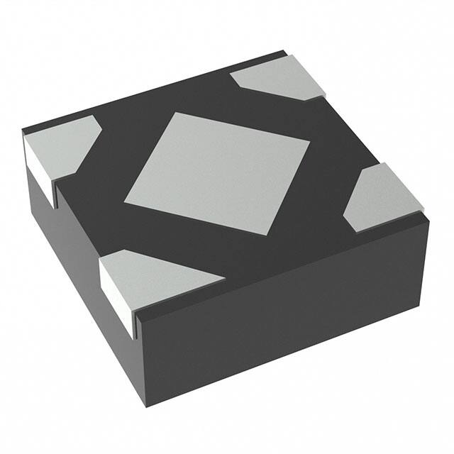
The RP130x supports two package types: DFN(PLP)1010-4 and SOT-23-5. By the adoption of the ultracompact DFN(PLP)1010-4, the RP130x can achieve a higher density mounting than ever.
This is a high-reliability semiconductor device for industrial applications (-Y) that has passed both the screening
at high temperature and the reliability test with extended hours.
FEATURES
Input Voltage Range (Max. Rating) ···················· 1.7V to 6.5V (7.0V)
Operating Temperature Range ························· - 40°C to 105°C
Supply Current·············································· Typ. 38µA
Supply Current (Standby Mode) ························ Typ. 0.1µA
Ripple Rejection ············································ Typ. 80dB (f = 1kHz)
Output Voltage Range ···································· 1.2V, 1.5V, 1.8V, 2.5V, 2.8V, 2.9V, 3.0V,
3.3V, 3.4V, 3.6V, 4.2V and 5.0V
Contact Ricoh sales representatives for other voltages.
Output Voltage Accuracy ································· ±1.0% (VSET > 2.0V, Ta = 25°C)
Temperature-Drift Coefficient of Output Voltage ···· Typ. ±20 ppm / °C
Dropout Voltage ············································ Typ. 0.32V (IOUT = 150mA, VSET = 2.8V)
Line Regulation ············································· Typ. 0.02% / V
Packages ···················································· DFN(PLP)1010-4, SOT-23-5
Built-in Fold Back Protection Circuit ··················· Typ. 40mA
Recommended Ceramic Capacitors ·················· 0.47µF or more
Output Noise Voltage ····································· Typ. VSET × 20 [µVrms]
(BW = 10Hz to 100kHz, IOUT = 30mA)
APPLICATIONS
Industrial equipments such as FAs and smart meters
Equipments used under high-temperature conditions such as surveillance camera and vending machine
Equipments accompanied by self-heating such as motor and lighting
1
�RP130x-Y
NO.EA-336-211001
BLOCK DIAGRAMS
RP130xxx1B
VDD
RP130xxx1D
VOUT
VDD
Vref
VOUT
Vref
Current Limit
Current Limit
CE
GND
CE
GND
SELECTION GUIDE
The output voltage, chip-enable polarity, auto-discharge function, and package type for this device can be
selected at the user’s request.
Product Name
RP130Kxx1∗-TR-Y
RP130Nxx1∗-TR-YE
Package
Quantity per
Reel
Pb Free
Halogen Free
DFN(PLP)1010-4
10,000pcs
Yes
Yes
SOT-23-5
3,000pcs
Yes
Yes
xx : Specify the set output voltage (VSET)
1.2 V (12) / 1.5 V (15) / 1.8 V (18) / 2.5 V (25) / 2.8 V (28) / 2.9 V (29) /
3.0 V (30) / 3.3 V (33) / 3.4 V (34) / 3.6 V (36) / 4.2 V (42) / 5.0 V (50)
Note: Contact Ricoh sales representatives for other voltages.
∗ : Specify the desired functions for chip-enable polarity and auto-discharge
B: "H" active / No auto-discharge function
D: "H" active / Auto-discharge function
Auto-Discharge function quickly lowers the output voltage to 0V by releasing the electrical charge in the external
capacitor when the chip enable signal is switched from the active mode to the standby mode.
2
�RP130x-Y
NO.EA-336-211001
PIN DESCRIPTION
• DFN(PLP)1010-4
Top View
4
3
• SOT-23-5
Bottom View
3
4
5
(mark side)
*1
1
2
2
4
1
1
2
3
DFN(PLP)1010-4
*1
Pin No.
Symbol
Description
1
VOUT
Output Pin
2
GND
Ground Pin
3
CE
Chip Enable Pin ("H" Active)
4
VDD
Input Pin
The tab on the bottom of the package enhances thermal performance and is electrically connected to GND (substrate
level). It is recommended that the tab be connected to the ground plane on the board, or otherwise be left floating.
SOT-23-5
Pin No.
Symbol
Description
1
VDD
2
GND
3
CE
Chip Enable Pin ("H" Active)
4
NC
No Connection
5
VOUT
Input Pin
Ground Pin
Output Pin
3
�RP130x-Y
NO.EA-336-211001
ABSOLUTE MAXIMUM RATINGS
Symbol
Item
Rating
Unit
VIN
Input Voltage
- 0.3 to 7.0
V
VCE
Input Voltage (CE Pin)
- 0.3 to 7.0
V
VOUT
Output Voltage
- 0.3 to VIN+0.3
V
IOUT
Output Current
200
mA
PD
Power Dissipation
Tj
Junction Temperature
- 40 to 125
°C
Strong Temperature Range
- 55 to 125
°C
Tstg
Refer to “PACKAGE INFORMATION”
ABSOLUTE MAXIMUM RATINGS
Electronic and mechanical stress momentarily exceeded absolute maximum ratings may cause
permanent damage and may degrade the life time and safety for both device and system using the
device in the field.
The functional operation at or over these absolute maximum rating is not assured.
RECOMMENDED OPERATING CONDITIONS
Symbol
Item
VIN
Input Voltage
Ta
Operating Temperature Range
Rating
Unit
1.7 to 6.5
V
- 40 to 105
°C
RECOMMENDED OPERATING CONDITIONS
All of electronic equipment should be designed that the mounted semiconductor devices operate within
the recommended operating conditions. The semiconductor devices cannot operate normally over the
recommended operating conditions, even if they are used over such conditions by momentary electronic
noise or surge. And the semiconductor devices may receive serious damage when they continue to
operate over the recommended operating conditions.
4
�RP130x-Y
NO.EA-336-211001
ELECTRICAL CHARACTERISTICS
VIN = VSET+1.0V (VSET > 1.5V), VIN = 2.5V (VSET ≤ 1.5V), IOUT = 1mA, CIN = COUT = 0.47µF, unless otherwise noted.
The specifications surrounded by
are guaranteed by design engineering at - 40ºC ≤ Ta ≤ 105ºC.
RP130xxx1B/D
Symbol
(Ta = 25°C)
Item
Conditions
Ta = 25°C
VOUT
Output Voltage
- 40°C ≤ Ta ≤ 105°C
IOUT
∆VOUT
/∆IOUT
VDIF
Min.
Dropout Voltage
Max.
Unit
VSET > 2.0V
×0.99
×1.01
V
VSET ≤ 2.0V
- 20
20
mV
VSET > 2.0V
×0.985
×1.015
V
VSET ≤ 2.0V
- 30
30
mV
Output Current
Load Regulation
Typ.
150
1mA ≤ IOUT ≤ 150mA
IOUT = 150mA
mA
10
30
1.2V ≤ VSET < 1.5V
0.67
1.03
1.5V ≤ VSET < 1.7V
0.54
0.84
1.7V ≤ VSET < 2.0V
0.46
0.75
2.0V ≤ VSET < 2.5V
0.41
0.63
2.5V ≤ VSET < 4.0V
0.32
0.51
4.0V ≤ VSET ≤ 4.2V
0.24
0.39
VSET = 5V
0.24
0.31
mV
V
ISS
Supply Current
IOUT = 0mA
38
58
µA
Istandby
Supply Current
(at Standby)
VCE = 0
0.1
1.0
µA
∆VOUT
/∆VIN
Line Regulation
VSET + 0.5V ≤ VIN ≤ 6.5V
0.02
0.10
%/V
ISC
Short Current Limit
VOUT = 0V
IPD
CE Pull-down Current
VCEH
CE Input Voltage "H"
VCEL
CE Input Voltage "L"
RLOW
Nch ON Resistance
for Auto Discharge
(D Version Only)
40
mA
0.4
µA
1.0
V
0.36
VIN = 4.0V, VCE = 0V
30
V
Ω
All test items listed under Electrical Characteristics are done under the pulse load condition (Tj ≈ Ta = 25°C)
5
�RP130x-Y
NO.EA-336-211001
Product-specific Electrical Characteristics
The specifications surrounded by
are guaranteed by design engineering at - 40ºC ≤ Ta ≤ 105ºC.
(Ta = 25°C)
Product Name
6
VOUT [V]
(Ta = 25°C)
VOUT [V]
(Ta = − 40 to 105°C)
VDIF [V]
Min.
Typ.
Max.
Min.
Typ.
Max.
Typ.
Max.
RP130x121x
1.180
1.200
1.220
1.170
1.200
1.230
0.67
1.03
RP130x151x
1.480
1.500
1.520
1.470
1.500
1.530
0.54
0.84
RP130x181x
1.780
1.800
1.820
1.770
1.800
1.830
0.46
0.75
RP130x251x
2.475
2.500
2.525
2.463
2.500
2.538
RP130x281x
2.772
2.800
2.828
2.758
2.800
2.842
RP130x291x
2.871
2.900
2.929
2.857
2.900
2.944
RP130x301x
2.970
3.000
3.030
2.955
3.000
3.045
0.32
0.51
RP130x331x
3.267
3.300
3.333
3.251
3.300
3.350
RP130x341x
3.366
3.400
3.434
3.349
3.400
3.451
RP130x361x
3.564
3.600
3.636
3.546
3.600
3.654
RP130x421x
4.158
4.200
4.242
4.137
4.200
4.263
0.24
0.39
RP130x501x
4.950
5.000
5.050
4.925
5.000
5.075
0.24
0.31
�RP130x-Y
NO.EA-336-211001
TYPICAL APPLICATION
VDD
C1
CE Control
VOUT
RP130x
CE
VOUT
C2
GND
External Components:
Symbol
Description
C2
0.47µF (Ceramic)
TECHNICAL NOTES
Phase Compensation
In the ICs, phase compensation is made for securing stable operation even if the load current is varied. For this
purpose, use a capacitor C2 with 0.47µF or more.
If a tantalum capacitor is used, and its ESR (Equivalent Series Resistance) of C2 is large, the loop oscillation
may result. Because of this, select C2 carefully considering its frequency characteristics.
PCB Layout
Make VDD and GND lines sufficient. If their impedance is too high, noise pickup or unstable operation may result.
Connect 0.47µF or more of the capacitor C1 between the VDD and GND, and as close as possible to the pins.
In addition, connect the capacitor C2 between VOUT and GND, and as close as possible to the pins.
7
�RP130x-Y
NO.EA-336-211001
TYPICAL APPLICATION FOR IC CHIP BREAKDOWN PREVENTION
VDD
C1
CE Control
VOUT
RP130x
CE
VOUT
C2
D1
GND
When a sudden surge of electrical current travels along the VOUT pin and GND due to a short-circuit, electrical
resonance of a circuit involving an output capacitor (C2) and a short circuit inductor generates a negative voltage
and may damage the device or the load devices. Connecting a schottky diode (D1) between the VOUT pin and
GND has the effect of preventing damage to them.
8
�RP130x-Y
NO.EA-336-211001
PACKAGE INFORMATION
Power Dissipation (DFN(PLP)1010-4)
PD-DFN(PLP)1010-4-(105125)-JE-B
The power dissipation of the package is dependent on PCB material, layout, and environmental conditions.
The following measurement conditions are based on JEDEC STD. 51-7.
Measurement Conditions
Item
Measurement Conditions
Environment
Mounting on Board (Wind Velocity = 0m/s)
Board Material
Glass Cloth Epoxy Plastic (Four-Layer Board)
Board Dimensions
76.2mm × 114.3mm × 0.8mm
Copper Ratio
Outer Layer (First Layer): Less than 95% of 50mm Square
Inner Layers (Second and Third Layers): Approx. 100% of 50mm Square
Outer Layer (Fourth Layer): Approx. 100% of 50mm Square
Through-holes
φ 0.2mm × 11pcs
Measurement Result
(Ta = 25°C, Tjmax = 125°C)
Item
Measurement Result
Power Dissipation
800mW
Thermal Resistance (θja)
θja = 125°C/W
Thermal Characterization Parameter (ψjt)
ψjt = 58°C/W
θja: Junction-to-Ambient Thermal Resistance
ψjt: Junction-to-Top Thermal Characterization Parameter
1000
900
800
Power Dissipation (mW)
800
700
600
500
400
300
200
100
0
0
25
50
75
100105
125
Ambient Temperature (°C)
Power Dissipation vs. Ambient Temperature
Measurement Board Pattern
9
�RP130x-Y
NO.EA-336-211001
Package Dimensions (DFN(PLP)1010-4)
DM-DFN(PLP)1010-4-JE-C
UNIT : mm
DFN(PLP)1010-4 Package Dimensions
10
�RP130x-Y
NO.EA-336-211001
● Mark Specifications (DFN(PLP)1010-4)
MK-RP130K-JYEY-A
: Product Code … Refer to “RP130K Mark Specification Table”
: Lot Number …Alphanumeric Serial Number
DFN(PLP)1010-4 Mark Specifications
RP130K Mark Specification Table (DFN(PLP)1010-4)
RP130Kxx1B
Product Name
VSET
RP130Kxx1D
Product
VSET
RP130K121B
TA
1.2 V
RP130K121D
VA
1.2 V
RP130K151B
TD
1.5 V
RP130K151D
VD
1.5 V
RP130K181B
TG
1.8 V
RP130K181D
VG
1.8 V
RP130K251B
TQ
2.5 V
RP130K251D
VQ
2.5 V
RP130K281B
TT
2.8 V
RP130K281D
VT
2.8 V
RP130K291B
TV
2.9 V
RP130K291D
VV
2.9 V
RP130K301B
TW
3.0 V
RP130K301D
VW
3.0 V
RP130K331B
TZ
3.3 V
RP130K331D
VZ
3.3 V
RP130K341B
UA
3.4 V
RP130K341D
WA
3.4 V
RP130K361B
UC
3.6 V
RP130K361D
WC
3.6 V
RP130K421B
UJ
4.2 V
RP130K421D
WJ
4.2 V
RP130K501B
US
5.0 V
RP130K501D
WS
5.0 V
11
�RP130x-Y
NO.EA-336-211001
Power Dissipation (SOT-23-5)
PD-SOT-23-5-(105125)-JE-B
The power dissipation of the package is dependent on PCB material, layout, and environmental conditions.
The following measurement conditions are based on JEDEC STD. 51-7.
Measurement Conditions
Item
Measurement Conditions
Environment
Mounting on Board (Wind Velocity = 0m/s)
Board Material
Glass Cloth Epoxy Plastic (Four-Layer Board)
Board Dimensions
76.2mm × 114.3mm × 0.8mm
Copper Ratio
Outer Layer (First Layer): Less than 95% of 50mm Square
Inner Layers (Second and Third Layers): Approx. 100% of 50mm Square
Outer Layer (Fourth Layer): Approx. 100% of 50mm Square
Through-holes
φ 0.3 mm × 7 pcs
Measurement Result
(Ta = 25°C, Tjmax = 125°C)
Item
Measurement Result
Power Dissipation
660mW
Thermal Resistance (θja)
θja = 150°C/W
Thermal Characterization Parameter (ψjt)
ψjt = 51°C/W
θja: Junction-to-Ambient Thermal Resistance
ψjt: Junction-to-Top Thermal Characterization Parameter
800
Power Dissipation PD (mW)
700
660
600
500
400
300
200
100
0
0
25
50
75
100 105
125
Ambient Temperature (°C)
Power Dissipation vs. Ambient Temperature
12
Measurement Board Pattern
�RP130x-Y
NO.EA-336-211001
Package Dimensions (SOT-23-5)
DM-SOT-23-5-JE-A
2.9±0.2
1.1±0.1
1.9±0.2
0.8±0.1
(0.95)
4
1
2
0~0.1
0.2min.
+0.2
1.6-0.1
5
2.8±0.3
(0.95)
3
0.4±0.1
+0.1
0.15-0.05
Unit : mm
SOT-23-5 Package Dimensions
13
�RP130x-Y
NO.EA-336-211001
Mark Specifications (SOT-23-5)
MK-RP130N-JYEY-A
: Product Code … Refer to “RP130N Mark Specification Table”
: Lot Number …Alphanumeric Serial Number
5
4
1
2
3
SOT-23-5 Mark Specifications
RP130N Mark Specification Table (SOT-23-5)
RP130Nxx1B
14
Product Name
VSET
RP130N121B
H1A
RP130N151B
RP130Nxx1D
Product Name
VSET
1.2 V
RP130N121D
H2A
1.2 V
H1D
1.5 V
RP130N151D
H2D
1.5 V
RP130N181B
H1G
1.8 V
RP130N181D
H2G
1.8 V
RP130N251B
H1Q
2.5 V
RP130N251D
H2Q
2.5 V
RP130N281B
H1T
2.8 V
RP130N281D
H2T
2.8 V
RP130N291B
H1V
2.9 V
RP130N291D
H2V
2.9 V
RP130N301B
H1W
3.0 V
RP130N301D
H2W
3.0 V
RP130N331B
H1Z
3.3 V
RP130N331D
H2Z
3.3 V
RP130N341B
J1A
3.4 V
RP130N341D
J2A
3.4 V
RP130N361B
J1C
3.6 V
RP130N361D
J2C
3.6 V
RP130N421B
J1J
4.2 V
RP130N421D
J2J
4.2 V
RP130N501B
J1S
5.0 V
RP130N501D
J2S
5.0 V
�RP130x-Y
NO.EA-336-211001
TEST CIRCUITS
VDD
VOUT
RP130x
C1
CE
V
C2
VOUT ↓
IOUT
GND
C1 = Ceramic 0.47µF
C2 = Ceramic 0.47µF
Standard Test Circuit
VDD
A
ISS
VOUT
VOUT
RP130x
C1
CE
C2
GND
C1 = Ceramic 0.47µF
C2 = Ceramic 0.47µF
Supply Current Test Circuit
VDD
Pulse
Generator
VOUT
RP130x
P.G.
CE
C2
↓
IOUT
GND
C2 = Ceramic 0.47µF
Ripple Rejection, Line Transient Response Test Circuit
VDD
C1
RP130x
CE
VOUT
VOUT
C2
GND
↓ IOUTa
↓ IOUTb
C1 = Ceramic 0.47µF
C2 = Ceramic 0.47µF
Load Transient Response Test Circuit
15
�RP130x-Y
NO.EA-336-211001
TYPICAL CHARACTERISTICS
Note: Typical Characteristics are intended to be used as reference data; they are not guaranteed.
1) Output Voltage vs. Output Current (C1 = C2 = 0.47µF, Ta = 25°C)
RP130x121x
RP130x281x
RP130x501x
2) Output Voltage vs. Input Voltage (C1 = C2 = 0.47µF, Ta = 25°C)
RP130x121x
16
RP130x281x
�RP130x-Y
NO.EA-336-211001
RP130x501x
3) Supply Current vs. Input Voltage (C1 = C2 = 0.47µF, Ta = 25°C)
RP130x121x
RP130x281x
RP130x501x
17
�RP130x-Y
NO.EA-336-211001
4) Output Voltage vs. Temperature (IOUT = 1mA, C1 = C2 = 0.47µF)
RP130x121x
RP130x281x
VIN=2.2V
1.24
2.84
1.23
2.83
1.22
1.21
1.20
1.19
1.18
1.17
VIN=3.8V
2.85
Output Voltage V OUT (V)
Output Voltage V OUT (V)
1.25
1.16
2.82
2.81
2.80
2.79
2.78
2.77
2.76
1.15
-40 -25
0
25
50
Temperature Ta (℃)
2.75
105
75
100
-40 -25
0
25
50
Temperature Ta (℃)
75
105
100
RP130x501x
VIN=6.0V
5.05
Output Voltage V OUT (V)
5.04
5.03
5.02
5.01
5.00
4.99
4.98
4.97
4.96
4.95
-40 -25
0
25
50
Temperature Ta (℃)
75
105
100
5) Supply Current vs. Temperature (IOUT = 0mA, C1 = C2 = 0.47µF)
RP130x121x
RP130x281x
VIN=2.2V
38
36
34
32
30
-40 -25
18
0
25
50
Temperature Ta (℃)
75
105
100
VIN=3.8V
40
Supply Current Iss (μA)
Supply Current Iss (μA)
40
38
36
34
32
30
-40 -25
0
25
50
Temperature Ta (℃)
75
105
100
�RP130x-Y
NO.EA-336-211001
RP130x501x
VIN=6.0V
Supply Current Iss (μA)
40
38
36
34
32
30
-40 -25
0
25
50
Temperature Ta (℃)
75
105
100
6) Dropout Voltage vs. Output Current (C1 = C2 = 0.47µF)
RP130x121x
RP130x281x
RP130x501x
19
�RP130x-Y
NO.EA-336-211001
7) Dropout Voltage vs. Set Output Voltage (C1 = C2 = 0.47µF)
8) Ripple Rejection vs. Input Bias Voltage (C1 = none, C2 = 0.47µF, Ripple = 0.2Vp-p, Ta = 25°C)
RP130x281x
RP130x281x
9) Ripple Rejection vs. Frequency (C1 = none, C2 = 0.47µF, Ripple = 0.2Vp-p, Ta = 25°C)
RP130x121x
20
RP130x281x
�RP130x-Y
NO.EA-336-211001
RP130x501x
10) Input Transient Response (IOUT = 30mA, tr = tf = 5µs, C1 = none, C2 = 0.47µF, Ta = 25°C)
RP130x121x
RP130x281x
RP130x501x
21
�RP130x-Y
NO.EA-336-211001
11) Load Transient Response (tr = tf = 0.5µs, C1 = C2 = 0.47µF, IOUT = 50mA 100mA, Ta =
25°C)
RP130x121x
RP130x281x
RP130x501x
12) Load Transient Response (tr = tf = 0.5µs, C1 = C2 = 0.47µF, IOUT = 1mA 150mA, Ta = 25°C)
RP130x121x
22
RP130x281x
�RP130x-Y
NO.EA-336-211001
RP130x501x
13) Rise Time with CE Pin (C1 = C2 = 0.47µF, Ta = 25°C)
RP130x121x
RP130x121x
RP130x121x
RP130x281x
23
�RP130x-Y
NO.EA-336-211001
RP130x281x
RP130x281x
RP130x501x
RP130x501x
RP130x501x
24
�RP130x-Y
NO.EA-336-211001
14) Fall Time with CE Pin in D-Version (C1 = C2 = 0.47µF, Ta = 25°C)
RP130x121D
RP130x121D
RP130x121D
RP130x281D
RP130x281D
RP130x281D
25
�RP130x-Y
NO.EA-336-211001
RP130x501D
RP130x501D
RP130x501D
15) Minimum Operating Voltage (C1 = C2 = 0.47µF)
Hatched area is available
for 1.2V output.
26
�RP130x-Y
NO.EA-336-211001
ESR vs. Output Current
The RP130x is recommended to use a ceramic type capacitor, but the RP130x can be used other capacitors of
the lower ESR type. The relation between the output current (IOUT) and the ESR of output capacitor is shown
below.
Measurement conditions
Frequency Band: 10Hz to 3MHz
Measurement Temperature: − 40°C to 85°C
Hatched area: Noise level is 40μV (average) or below
Ceramic Capacitor: C1 = Ceramic 0.47μF, C2 = 0.47μF
RP130x121x
RP130x281x
V IN=1.4V to 6.5V
100
Ta=85℃
10
Ta=85℃
10
Ta=-40℃
ESR (Ω)
ESR (Ω)
V IN=3.0V to 6.5V
100
1
0.1
Ta=-40℃
1
0.1
0.01
0.01
0
25
50
75
100
125
Output Current IOUT (mA)
150
0
25
50
75
100 125
Output Current lOUT (mA)
150
RP130x501x
V IN=5.2V to 6.5V
100
Ta=85℃
10
ESR (Ω)
Ta=-40℃
1
0.1
0.01
0
25
50
75
100
125
Output Current lOUT (mA)
150
27
�1. The products and the product specifications described in this document are subject to change or discontinuation of
production without notice for reasons such as improvement. Therefore, before deciding to use the products, please
refer to Ricoh sales representatives for the latest information thereon.
2. The materials in this document may not be copied or otherwise reproduced in whole or in part without prior written
consent of Ricoh.
3. Please be sure to take any necessary formalities under relevant laws or regulations before exporting or otherwise
taking out of your country the products or the technical information described herein.
4. The technical information described in this document shows typical characteristics of and example application circuits
for the products. The release of such information is not to be construed as a warranty of or a grant of license under
Ricoh's or any third party's intellectual property rights or any other rights.
5. The products listed in this document are intended and designed for use as general electronic components in standard
applications (office equipment, telecommunication equipment, measuring instruments, consumer electronic products,
amusement equipment etc.). Those customers intending to use a product in an application requiring extreme quality
and reliability, for example, in a highly specific application where the failure or misoperation of the product could result
in human injury or death (aircraft, spacevehicle, nuclear reactor control system, traffic control system, automotive and
transportation equipment, combustion equipment, safety devices, life support system etc.) should first contact us.
6. We are making our continuous effort to improve the quality and reliability of our products, but semiconductor products
are likely to fail with certain probability. In order to prevent any injury to persons or damages to property resulting from
such failure, customers should be careful enough to incorporate safety measures in their design, such as redundancy
feature, fire containment feature and fail-safe feature. We do not assume any liability or responsibility for any loss or
damage arising from misuse or inappropriate use of the products.
7. Anti-radiation design is not implemented in the products described in this document.
8. The X-ray exposure can influence functions and characteristics of the products. Confirm the product functions and
characteristics in the evaluation stage.
9. WLCSP products should be used in light shielded environments. The light exposure can influence functions and
characteristics of the products under operation or storage.
10. There can be variation in the marking when different AOI (Automated Optical Inspection) equipment is used. In the
case of recognizing the marking characteristic with AOI, please contact Ricoh sales or our distributor before attempting
to use AOI.
11. Please contact Ricoh sales representatives should you have any questions or comments concerning the products or
the technical information.
Halogen Free
Ricoh is committed to reducing the environmental loading materials in electrical devices
with a view to contributing to the protection of human health and the environment.
Ricoh has been providing RoHS compliant products since April 1, 2006 and Halogen-free products since
April 1, 2012.
Official website
https://www.n-redc.co.jp/en/
Contact us
https://www.n-redc.co.jp/en/buy/
�


 工商网监
湘ICP备2023018690号
工商网监
湘ICP备2023018690号