RP154x Series
300 mA Ultra-small Dual LDO Regulator
No. EA-202-171005
OUTLINE
The RP154x is a CMOS-based voltage regulator that provides high ripple rejection, low dropout voltage, high
output voltage accuracy, and low supply current. Internally, the RP154x consists of a voltage reference unit,
an error amplifier, resistors for setting output voltage, a short current limit circuit and a chip enable circuit.
The RP154x is available in fixed output voltage options. Besides the low supply current by CMOS, the RP154x
offers a low dropout voltage by built-in low ON resistance Tr. as well as an extended battery life by a chip
enable function. Compared with the existing CMOS-based regulators, the RP154x is further improved in ripple
rejection, line transient response, and load transient response. All these features allow the RP154x to become
ideal power sources for hand-held communication equipment.
The RP154x is offered in a 6-pin SOT-23-6 package for a single input type and an 8-pin DFN1216-8 package
for a dual input type. Both packages are equipped with two LDOs which can achieve high-density mounting.
FEATURES
•
•
•
•
•
•
•
•
•
•
•
•
•
Supply Current ..................................................................... Typ. 50 µA x 2 (VR1 & VR2)
Standby Current ................................................................... Typ. 0.1µA x 2 (VR1 & VR2)
Input Voltage Range............................................................. 1.4 V to 5.25 V
Output Voltage Range .......................................................... 0.8 V to 3.7 V (0.1 V steps)
Output Voltage Accuracy ...................................................... ±1.0% (VSET > 2.0 V, Ta = 25°C)
Temperature-Drift Coefficient of Output Voltage .................. Typ. ±80 ppm/°C
Dropout Voltage ................................................................... Typ. 0.25 V (IOUT = 300 mA, VSET = 2.5 V)
Ripple Rejection ................................................................... Typ. 75 dB (f = 1 kHz)
Line Regulation .................................................................... Typ. 0.02%/V
Packages ............................................................................ DFN1216-8, SOT-23-6
Short-current Limit Circuit .................................................... Typ. 60 mA
Overcurrent Protection Circuit
Ceramic Capacitor Compatible ............................................ 1.0 µA or more
APPLICATIONS
•
•
•
Power source for portable communication equipment.
Power source for electrical appliances such as cameras, VCRs and camcorders.
Power source for battery-powered equipment.
1
�RP154x
No. EA-202-171005
SELECTION GUIDE
The set output voltage, the package type and the auto discharge function(1) are user-selectable options.
Selection Guide
Product Name
RP154L0xx∗-E2
Package
Quantity per Reel
Pb Free
Halogen Free
DFN1216-8
5,000 pcs
Yes
Yes
SOT-23-6
3,000 pcs
Yes
Yes
RP154N0xx∗-TR-FE
xx: Specify the combination of set output voltage (VSET) within the range of 0.8 V to 3.7 V in 0.1 V step. .
∗: The auto discharge function at off state are options as follows.
(A) Auto-discharge function included, Active-high
(B) Auto-discharge function not included, Active-high
BLOCK DIAGRAMS
CE1
VOUT1
R1_1
Error Amp.
Vref
R2_1
Current Limit
VDD
GND
R1_2
Error Amp.
Vref
R2_2
Current Limit
CE2
VOUT2
RP154NxxxA Block Diagram
(1) Auto-discharge function quickly lowers the output voltage to 0 V by releasing the electrical charge accumulated in the
external capacitor when the chip enable signal is switched from the active mode to the standby mode.
2
�RP154x
No. EA-202-171005
CE1
VOUT1
R1_1
Error Amp.
Vref
R2_1
Current Limit
VDD
GND
R1_2
Error Amp.
Vref
R2_2
Current Limit
CE2
VOUT2
RP154NxxxB Block Diagram
VDD1
VOUT1
R1_1
Error Amp.
Vref
R2_1
Current Limit
CE1
GND
VDD2
R1_2
Error Amp.
Vref
R2_2
Current Limit
CE2
VOUT2
RP154LxxxA Block Diagram
3
�RP154x
No. EA-202-171005
VDD1
VOUT1
R1_1
Error Amp.
Vref
R2_1
Current Limit
CE1
GND
VDD2
R1_2
Error Amp.
Vref
R2_2
Current Limit
CE2
VOUT2
RP154LxxxB Block Diagram
4
�RP154x
No. EA-202-171005
PIN DESCRIPTIONS
8
7
6
6
Bottom View
Top View
5
5
6
7
2
3
4
4
4
8
(mark side)
(1)
1
5
3
2
1
DFN1216-8 Pin Configuration
1
1
2
3
SOT-23-6 Pin Configuration
DFN1216-8 Pin Description
Pin No.
Symbol
Description
Ground
Pin(2)
1
GND
2
VOUT1
Output Pin 1
3
VOUT2
Output Pin 2
4
GND
Ground Pin(2)
5
CE2
Chip Enable Pin 2, Active-high
6
VDD2
Input Pin
7
VDD1
Input Pin
8
CE1
Chip Enable Pin 1, Active-high
SOT-23-6 Pin Description
Pin No.
Symbol
Description
1
CE1
Chip Enable Pin 1 ("H" Active)
2
VDD
Input Pin
3
CE2
Chip Enable Pin 2 ("H" Active)
4
VOUT2
Output Pin 2
5
GND
Ground Pin
6
VOUT1
Output Pin 1
(1) Tab is GND level. (They are connected to the reverse side of this IC). The tab is better to be connected to the GND,
but leaving it open is also acceptable.
(2) The GND pin must be wired together when it is mounted on board.
5
�RP154x
No. EA-202-171005
ABSOLUTE MAXIMUM RATINGS
Absolute Maximum Ratings
Symbol
Item
VIN
Input Voltage
VCE
Input Voltage (CE Pin)
Rating
Unit
6.0
V
−0.3 to 6.0
V
VOUT1, VOUT2
Output Voltage
−0.3 to VIN +0.3
V
IOUT1, IOUT2
Output Current
400
mA
PD
PD
Power Dissipation(1)
(JEDEC STD. 51-7 Test Land Pattern)
DFN1216-8
1700
SOT-23-6
660
Power Dissipation (DFN1216-8)(2)
625
Power Dissipation (SOT-23-6)(1)
420
mW
mW
Tj
Junction Temperature Range
−40 to 125
°C
Tstg
Storage Temperature Range
−55 to 125
°C
ABSOLUTE MAXIMUM RATINGS
Electronic and mechanical stress momentarily exceeded absolute maximum ratings may cause the permanent
damages and may degrade the life time and safety for both device and system using the device in the field. The
functional operation at or over these absolute maximum ratings is not assured.
RECOMMENDED OPERATING CONDITIONS
Recommended Operating Conditions
Symbol
Item
Rating
Unit
VIN
Operating Input Voltage
1.4 to 5.25
V
Ta
Operating Temperature Range
−40 to 85
°C
RECOMMENDED OPERATING CONDITIONS
All of electronic equipment should be designed that the mounted semiconductor devices operate within the
recommended operating conditions. The semiconductor devices cannot operate normally over the recommended
operating conditions, even if when they are used over such conditions by momentary electronic noise or surge. And
the semiconductor devices may receive serious damage when they continue to operate over the recommended
operating conditions.
(1)
(2)
6
Refer to POWER DISSIPATION for detailed information.
Refer to POWER DISSIPATION for detailed information.
�RP154x
No. EA-202-171005
ELECTRICAL CHARACTERISTICS
VIN = VSET > +1.0 V (VSET > 1.5 V), VIN = 2.5 V (VSET ≤ 1.5 V), IOUT = 1 mA, CIN = COUT = 1.0 µF, unless otherwise noted,
VSET = Set Output Voltage
is checked and guranteed by design engineering at −40°C ≤ Ta ≤ 85°C.
The specification in
VR1/VR2 Electrical Characteristics
Symbol
(Ta = 25°C)
Item
Conditions
Ta = 25°C
VOUT
Output Voltage
−40°C ≤ Ta ≤ 85°C
IOUT
Min.
Typ.
Max.
Unit
VSET > 2.0 V
×0.99
×1.01
V
VSET ≤ 2.0 V
−20
20
mV
VSET > 2.0 V
×0.97
×1.03
V
VSET ≤ 2.0 V
−60
60
mV
Output Current
mA
300
∆VOUT
/∆IOUT
Load Regulation
VDIF
Dropout Voltage
ISS
Supply Current
IOUT = 0 mA
50
75
µA
Istandby
Standby Current
VCE = 0 V
0.1
1.0
µA
∆VOUT
/∆VIN
Line Regulation
VSET + 0.5 V ≤ VIN ≤ 5.25 V (VIN ≥ 1.4 V)
0.02
0.10
%/V
RR
Ripple Rejection
f = 1 kHz, Ripple 0.2 Vp-p
VIN = VSET+1.0 V, IOUT = 30 mA
(When VSET ≤ 2.0 V, VIN = 3.0 V)
VIN
Input Voltage(1)
∆VOUT
/∆Ta
Output Voltage
Temperature
Coefficient
−40°C ≤ Ta ≤ 85°C
±80
ppm
/°C
ISC
Short Current Limit
VOUT = 0 V
60
mA
IPD
CE Pull-down Current
VCEH
CE Input Voltage "H"
VCEL
CE Input Voltage "L"
en
RLOW
1 mA ≤ IOUT ≤ 300 mA
15
40
mV
Refer to Dropout Voltage by Set Output Voltage.
75
1.4
dB
5.25
0.3
0.6
V
µA
V
1.0
0.4
V
Output Noise
BW = 10 Hz ∼ 100 kHz
75
µVrms
Low Output Nch Tr.
ON Resistance
(of B version)
VIN = 4.0 V, VCE = 0 V
50
Ω
All of unit are tested and specified under load conditions such that Tj ≈ Ta = 25°C except for Output Noise, Ripple Rejection,
Output Voltage Temperature Coefficient and Thermal Shutdown.
(1) The maximum Input Voltage of ELECTRICAL CHARACTERISTICS is 5.25 V. In case of exceeding this specification,
the IC must be operated on condition that the Input Voltage is up to 5.5 V and the total operating time is within 500 hrs.
7
�RP154x
No. EA-202-171005
ELECTRICAL CHARACTERISTICS (continued)
The specification in
is checked and guranteed by design engineering at −40°C ≤ Ta ≤ 85°C.
Dropout Voltage by Set Output Voltage
Set Output Voltage
VSET (V)
Dropout Voltage VDIF (V)
Typ.
Max.
VSET = 0.8
0.56
0.72
VSET = 0.9
0.51
0.65
1.0 ≤ VSET < 1.2
0.46
0.59
1.2 ≤ VSET
很抱歉,暂时无法提供与“RP154L041B-E2”相匹配的价格&库存,您可以联系我们找货
免费人工找货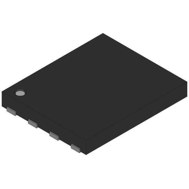


 工商网监
湘ICP备2023018690号
工商网监
湘ICP备2023018690号