RP202x SERIES
Low Power / Fast Mode Alternative 200mA LDO Regulator
NO.EA-279-170710
OUTLINE
The RP202x is voltage regulator IC with high output voltage accuracy, low dropout voltage and low supply
current. This IC performs with the chip enable function and realize a standby mode with low supply current. To
prevent the destruction by over current, the current limit circuit is included. The RP202x has 3-mode. One is
standby mode with CE pin. The other two are the fast response mode (Fast Mode) and the low power mode,
and switch over automatically according to the load current of the LDO. Supply current of IC itself at light load
is automatically reduced. The output voltage is maintained between Fast Mode and ECO Mode.
The RP202x consists of a voltage reference unit, an error amplifier, a resister net for voltage setting, and a
current limit circuit.
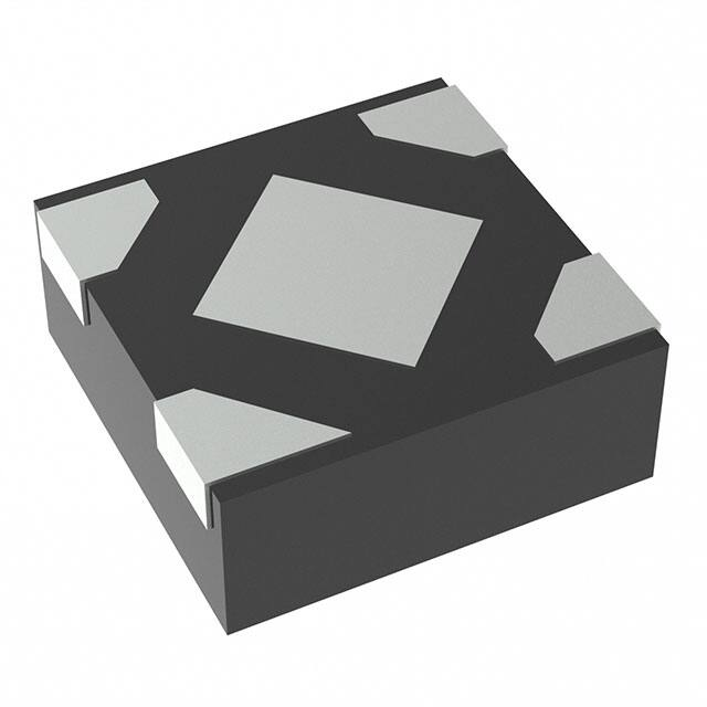
Since the packages are SOT-23-5, SC-88A, and DFN(PLP)1010-4, high density mounting of the IC on boards
is possible.
FEATURES
Input Voltage Range ······································· 1.4V to 5.25V
Output Voltage Range ····································· 0.8V to 4.0V (0.1V steps)
Supply Current (IOUT=0mA) ······························· Typ. 2.5µA
Supply Current (IOUT=10mA) ······························ Typ. 50µA
Supply Current (Standby Mode) ························· Typ. 0.1µA
Dropout Voltage ············································· Typ. 0.20V (IOUT=200mA, VOUT=2.8V)
Ripple Rejection ············································· Typ. 70dB (f=1kHz, VOUT=2.8V, IOUT=30mA)
Line Regulation ·············································· Typ. 0.02%/V (IOUT=10mA)
Packages ····················································· DFN(PLP)1010-4, SC-88A, SOT-23-5
Built-in Foldback Protection Circuit ····················· Typ. 60mA (Current at short mode)
Built-in Constant Slope Circuit (Soft-start Function)
Ceramic capacitors are recommended to be used with this IC 0.47µF or more
APPLICATIONS
Power source for portable communication equipment.
Power source for electrical appliances such as cameras, VCRs and camcorders.
Power source for battery-powered equipment.
1
�RP202x
NO.EA-279-170710
SELECTION GUIDE
The output voltage, auto discharge function(1), and package, for the IC can be selected at the user’s request.
Product Name
Package
Quantity per Reel
Pb Free
Halogen Free
DFN(PLP)1010-4
10,000pcs
Yes
Yes
RP202Qxx2∗-TR-FE
SC-88A
3,000pcs
Yes
Yes
RP202Nxx1∗-TR-FE
SOT-23-5
3,000pcs
Yes
Yes
RP202Kxx1∗-TR
xx : The output voltage can be designated in the range from 0.8V(08) to 4.0V(40) in 0.1V steps.
∗ : The auto discharge function at off state are options as follows.
(B) without auto discharge function at off state
(D) with auto discharge function at off state
BLOCK DIAGRAMS
RP202xxxxB
VDD
RP202xxxxD
VOUT
VDD
Vref
Vref
Current Limit
CE
(1)
VOUT
Current Limit
GND
CE
GND
Auto-discharge function quickly lowers the output voltage to 0V, when the chip enable signal is switched from the
active mode to the standby mode, by releasing the electrical charge accumulated in the external capacitor.
2
�RP202x
NO.EA-279-170710
PIN DESCRIPTIONS
DFN(PLP)1010-4
Top View
Bottom View
SC-88A
4
5
4
3
3
2
5
4
4
∗
1
SOT-23-5
2
(mark side)
1
1
2
3
(mark side)
1
2
3
DFN(PLP)1010-4
Pin No
Symbol
Pin Description
1
VOUT
Output Pin
2
GND
Ground Pin
3
CE
Chip Enable Pin ("H" Active)
4
VDD
Input Pin
∗ Tab is GND level. (They are connected to the reverse side of this IC.) The tab is better to be connected to the GND, but
leaving it open is also acceptable.
SC-88A
Pin No
Symbol
1
CE
Chip Enable Pin ("H" Active)
NC
No Connection
2
(1)
Pin Description
3
GND
Ground Pin
4
VOUT
Output Pin
5
VDD
Input Pin
SOT-23-5
Pin No
Symbol
Pin Description
1
VDD
2
GND
3
CE
Chip Enable Pin ("H" Active)
4
NC
No Connection
5
VOUT
Output Pin
Input Pin
Ground Pin
(1)
Pin No. 2 is connected to the bottom of the IC. It is recommended that the pin be connected to the ground plane on
the board, or otherwise be left floating so that there is no contact with other potentials.
3
�RP202x
NO.EA-279-170710
ABSOLUTE MAXIMUM RATINGS
Symbol
Item
Rating
Unit
6.0
V
−0.3 to 6.0
V
VIN
Input Voltage
VCE
Input Voltage (CE Pin)
VOUT
Output Voltage
−0.3 to VIN + 0.3
V
IOUT
Output Current
220
mA
Power Dissipation (DFN(PLP)1010-4, Standard Test Land Pattern)
Power Dissipation (SC-88A, Standard Test Land Pattern) 1
PD
Power Dissipation (SOT-23-5, Standard Test Land Pattern)
1
400
380
1
mW
420
Tj
Junction Temperature Range
−40 to 125
°C
Tstg
Storage Temperature Range
−55 to 125
°C
ABSOLUTE MAXIMUM RATINGS
Electronic and mechanical stress momentarily exceeded absolute maximum ratings may cause the
permanent damages and may degrade the life time and safety for both device and system using the
device in the field. The functional operation at or over these absolute maximum ratings is not assured.
RECOMMENDED OPERATING CONDITIONS
Symbol
Item
Rating
Unit
VIN
Input Voltage
1.4 to 5.25
V
Ta
Operating Temperature Range
−40 to 85
°C
RECOMMENDED OPERATING CONDITIONS
All of electronic equipment should be designed that the mounted semiconductor devices operate within the
recommended operating conditions. The semiconductor devices cannot operate normally over the recommended
operating conditions, even if when they are used over such conditions by momentary electronic noise or surge. And
the semiconductor devices may receive serious damage when they continue to operate over the recommended
operating conditions.
(1)
4
Refer to POWER DISSIPATION for detailed information.
�RP202x
NO.EA-279-170710
ELECTRICAL CHARACTERISTICS
VIN=Set VOUT +1V, IOUT=1mA, CIN=COUT =0.47µF, unless otherwise noted.
The specification in
is checked and guaranteed by design engineering at -40°C≤Ta≤85°C.
Symbol
VOUT
IOUT
∆VOUT
/∆IOUT
VDIF
ISS1
ISS2
Item
Output Voltage
IOUTL
∆VOUT
/∆VIN
RR
IOUT=5mA (Fast Mode) VOUT > 2.0V
Ta=25°C
VOUT ≤ 2.0V
IOUT=5mA (Fast Mode) VOUT > 2.0V
-40°C ≤ Ta ≤ 85°C
VOUT ≤ 2.0V
Output Current
CE Pull-down
Constant Current
VCEH
CE Input Voltage “H”
VCEL
CE Input Voltage “L”
RLOW
Low Output Nch Tr.
ON Resistance
(of D version)
×1.01
-20mV
20mV
×0.965
×1.025
−70mV
50mV
V
mA
%
VOUT ≤ 2.0V
−20
20
mV
10
30
mV
IOUT=0mA
2.5
5.0
µA
IOUT=10mA
50
VCE=GND
0.1
−20
Refer to the "Dropout Voltage"
Fast Mode
IOUT= Light load to Heavy load
switch-over current
Low Power Mode
IOUT= Heavy load to Light load
switch-over current
IOUT=1mA
VOUT+0.5V ≤ VIN ≤ 5V (Low Power Mode)
Line Regulation
1.4V ≤ VIN
IOUT=10mA
(Fast Mode)
VOUT ≤ 1.8V
f=1kHz
1.8< VOUT ≤2.8V
Ripple 0.2Vp-p
Ripple Rejection
VIN=VOUT+1.0V,
2.8< VOUT ≤3.3V
IOUT=30mA
3.3 < VOUT
ICEPD
× 0.99
Unit
1.0
Dropout Voltage
Short Current Limit
Max.
−1.0
10mA ≤ IOUT ≤ 200mA
ISC
Typ.
VOUT > 2.0V
Load Regulation
Supply Current
(IOUT=0mA)(1)
Supply Current
(IOUT=10mA)
Min.
200
1mA ≤ IOUT ≤ 10mA
Istandby Standby Current
IOUTH
Conditions
(Ta=25°C)
1.0
µA
1.0
µA
8.0
mA
2.0
mA
±0.50
%/V
±0.02
VOUT=0V
±0.10
75
70
65
60
dB
60
mA
0.3
0.6
1.0
V
0.4
VIN = 4.0V
VCE = 0V
µA
60
V
Ω
All of units are tested and specified under load conditions such that Tj≈Ta25°C except for Ripple Rejection, Output Voltage
Temperature Coefficient.
(1)
The value of supply current is excluding the Pull-down constant current of CE Pin.
5
�RP202x
NO.EA-279-170710
Dropout Voltage
Output Voltage
VOUT (V)
Dropout Voltage
VDIF (V)
Typ.
Max.
0.8 ≤ VOUT
很抱歉,暂时无法提供与“RP202K271D-TR”相匹配的价格&库存,您可以联系我们找货
免费人工找货