RP300x Series
0.8% Accuracy, Voltage Detector with Delay Function
NO.EA-306-160309
OUTLINE
The RP300x is a CMOS-based voltage detector (VD) IC with a built-in output delay circuit. Internally, a single
IC consists of a voltage reference unit, a comparator, a resistor net for setting detector threshold, a manual
reset circuit, an output delay circuit and an output driver transistor.
The RP300x is available in internally fixed detector threshold type. When the VDD voltage becomes lower than
the preset voltage, the RP300xxxxA/C generates a “L” reset signal and the RP300xxxxB (custom IC*1)
generates a “H” reset signal. The detector threshold accuracy is as high as ±1.0% when −VSET*2 < 1.7 V and
±0.8% when 1.7 V ≤ −VSET.
The reset output signal remains asserted for 50 ms, 100 ms (custom IC) or 200 ms after the VDD voltage rises
above the threshold voltage or when manual reset is canceled. The RP300x is designed to ignore fast
transients on the VDD pin. The output delay time accuracy is as high as ±5.0%.
The RP300x is available in an Nch open drain output type or in a CMOS output type.
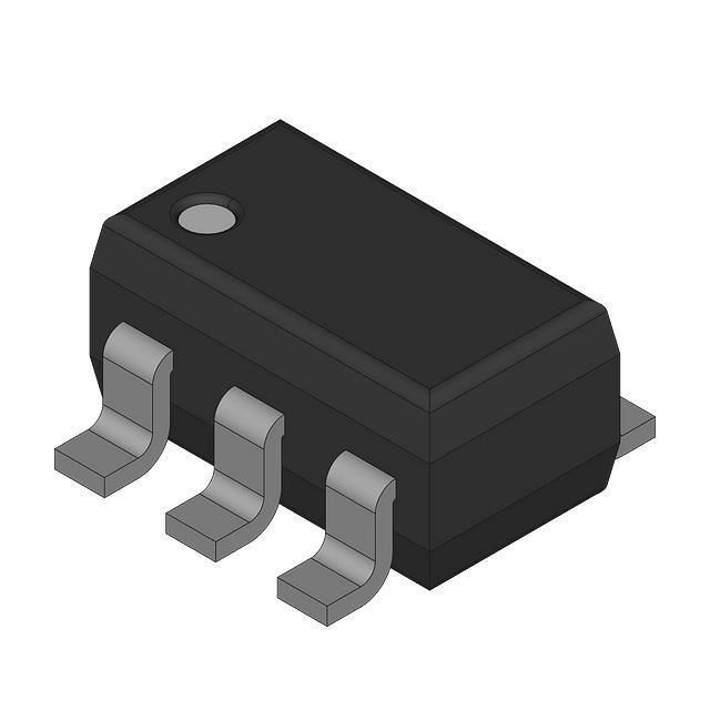
The RP300x is offered in an ultra-small DFN(PLP)1010-4B package or in a SOT-23-5 package.
*1
*2
For more information about a custom IC, please contact our sales representatives.
−VSET is defined as a preset detector threshold.
FEATURES
•
•
•
•
•
•
•
•
•
•
Supply Current ··············································· Typ. 0.95 µA (−VSET = 3.08 V, VDD = 3.18 V)
Operating Voltage Range ·································· 0.72 V to 5.50 V (25°C)
Detector Threshold Range ································ 1.1 V, 2.32 V, 2.63 V, 2.7 V, 2.8 V, 2.93 V, 3.08 V, 3.4 V (34),
4.38 V (43), 4.6 V (46)
Detector Threshold Accuracy ····························· ±1.0% (−VSET < 1.7 V), ±0.8% (1.7 V ≤ −VSET)
Detector Threshold Temperature Coefficient ·········· Typ. ±50 ppm/°C
Released Output Delay Time ····························· Typ. 50 ms, 100 ms (custom IC), 200 ms
Released Output Delay Time Accuracy ················ ±5% (25°C), ±15% (−40°C to 85°C)
Package ························································ DFN(PLP)1010-4B, SOT-23-5
Output Type ··················································· Nch Open Drain output, CMOS Output
Reset Signal ·················································· Active-low, Active-high (custom IC)
APPLICATIONS
•
•
Voltage monitoring for handheld communication equipment, camera and VCRs.
Voltage monitoring for battery-powered equipment
1
�RP300x
NO.EA-306-160309
BLOCK DIAGRAMS
Figure 1. RP300xxxxA/B (Nch Open Drain Output)
Figure 2. RP300xxxxC (CMOS Output)
SELECTION GUIDE
With the RP300x, the detector threshold, the package type, the released output delay time and the output type
are user-selectable options.
Product Name
RP300Kxxy∗(z)-TR
RP300Nxxy∗(z)-TR-FE
Package
DFN(PLP)1010-4B
SOT-23-5
Quantity per Reel
10,000 pcs
3,000 pcs
Pb Free
Yes
Yes
Halogen Free
Yes
Yes
xx: Specify −VSET from 1.1 V (11), 2.32 V (23), 2.63 V (26), 2.7 V (27), 2.8 V (28), 2.93 V (29),
3.08 V (30), 3.4 V (34), 4.38 V (43), 4.6 V (46).
z: If −VSET includes the 3rd digit, indicate the digit of 0.01 V.
Ex. If −VSET is 2.63 V, indicate as RP300x26xx3-TR-x.
y: Specify the released output delay time.
(A) 50 ms
(B) 100 ms (custom IC)
(D) 200 ms
∗: Specify the output type.
(A) Nch Open Drain Output
(B) Nch Open Drain Inverting Output (custom IC)
(C) CMOS Output
2
�RP300x
NO.EA-306-160309
PIN CONFIGULATIONS
• DFN(PLP)1010-4B
4
3
3
• SOT- 23-5
4
5
4
(mark side)
1
2
2
1
1
Figure 3. Top View
Figure 4. Bottom View
2
3
Figure 5. Mark Side
PIN DESCRIPTION
RP300K: DFN(PLP)1010-4B
Pin No.
Symbol
Pin Description
1
OUT
Output Pin
RP300xxxxA/C: asserts an active-low reset signal when a
voltage drops below the detector threshold.
RP300xxxxB: asserts an active-high reset signal when a
voltage drops below the detector threshold. (custom IC)
2
MR
Manual Reset Input Pin: active-low
3
GND
4
VDD
Ground Pin
Input Pin
The tab on the bottom of the package enhances thermal performance and is electrically connected to GND (substarate
level). It is recommended that the tab be connected to the ground plane on the board. If not, the tab can be left open.
RP300N: SOT-23-5
Pin No.
Symbol
1
MR
2
GND
3
NC
Description
Manual Reset Input Pin: active-low
Ground Pin
No Connection
4
OUT
Output Pin
RP300xxxxA/C: asserts an active-low reset signal when a
voltage drops below the detector threshold.
RP300xxxxB: asserts an active-high reset signal when a
voltage drops below the detector threshold. (custom IC)
5
VDD
Input Pin
3
�RP300x
NO.EA-306-160309
ABSOLUTE MAXIMUM RATINGS
Symbol
VIN
OUT
Rating
Unit
6.0
V
Output Voltage (Nch Open Drain Output)
−0.3 to 6.0
Output Voltage (CMOS Output)
−0.3 to VDD +0.3
MR
Manual Reset Pin
−0.3 to VDD +0.3
IOUT
Output Current
V
V
20
mA
DFN(PLP)1010-4B
400
SOT-23-5
420
PD
Power Dissipation (Standard Land Pattern)*3
Ta
Operating Temperature Range
−40 to +85
°C
Storage Temperature Range
−55 to +125
°C
Tstg
*3
Item
Input Voltage
mW
Refer to the next page for detailed information about Power Dissipation.
ABSOLUTE MAXIMUM RATINGS
Electronic and mechanical stress momentarily exceeded absolute maximum ratings may cause the permanent
damages and may degrade the life time and safety for both device and system using the device in the field. The
functional operation at or over these absolute maximum ratings is not assured.
RECOMMENDED OPERATING CONDITIONS (ELECTRICAL CHARACTERISTICS)
All of electronic equipment should be designed that the mounted semiconductor devices operate within the
recommended operating conditions. The semiconductor devices cannot operate normally over the recommended
operating conditions, even if when they are used over such conditions by momentary electronic noise or surge. And the
semiconductor devices may receive serious damage when they continue to operate over the recommended operating
conditions.
4
�RP300x
NO.EA-306-160309
POWER DISSIPATION (DFN(PLP)1010-4B)
Power Dissipation (PD) of the package is dependent on PCB material, layout, and environmental
conditions. The following conditions are used in this measurement.
Measurement Conditions
Standard Land Pattern
Environment
Mounting on Board (Wind Velocity = 0 m/s)
Board Material
Glass Cloth Epoxy Plastic (Double-sided)
Board Dimensions
40 mm x 40 mm x 1.6 mm
Copper Ratio
Top side: Approx. 50%, Back side: Approx. 50%
Through-holes
φ 0.54 mm x 24 pcs
(Ta = 25°C, Tjmax = 125°C)
Measurement Result:
Standard Land Pattern
Power Dissipation
400 mW
θja = (125 −25°C) / 0.4 W = 250°C/W
Thermal Resistance
θjc = 67°C/W
40
500
On Board
400
300
40
Power Dissipation PD (mW)
600
200
100
0
0
25
50
75 85 100
125
Ambient Temperature (°C)
Power Dissipation
150
Measurement Board Pattern
IC Mount Area (Unit : mm)
5
�RP300x
NO.EA-306-160309
POWER DISSIPATION (SOT-23-5)
Power Dissipation (PD) of the package is dependent on PCB material, layout, and environmental conditions.
The following conditions are used in this measurement. This data is taken from SOT-23-6.
Measurement Conditions
Standard Land Pattern
Environment
Mounting on Board (Wind Velocity = 0 m/s)
Board Material
Glass Cloth Epoxy Plastic (Double-sided)
Board Dimensions
40 mm x 40 mm x 1.6 mm
Copper Ratio
Top side: Approx. 50%, Back side: Approx. 50%
Through-holes
φ 0.5 mm x 44 pcs
(Ta = 25°C, Tjmax = 125°C)
Measurement Result:
Standard Land Pattern
Free Air
Power Dissipation
420 mW
250 mW
Thermal Resistance
θja = (125 − 25°C) / 0.42 W = 238°C/W
400°C/W
Power Dissipation PD (mW)
600
500
On Board
420
400
300
Free Air
250
200
100
0
0
25
50
75 85 100
125
Ambient Temperature (°C)
Power Dissipation
6
150
�RP300x
NO.EA-306-160309
ELECTRICAL CHARACTERISTICS
The specifications surrounded by
RP300x
Symbol
are guaranteed by design engineering at −40°C ≤ Ta ≤ 85°C.
(Ta = 25°C)
Conditions
*4
−VSET < 1.7 V
1.7 V ≤ −VSET
Min. Typ. Max. Unit
×0.99
×1.010
V
×0.992
×1.008
V
Detector Threshold
(−40°C ≤ Ta ≤ 85°C)
−VSET < 1.7 V
×0.982
×1.018
V
1.7 V ≤ −VSET
×0.984
×1.016
V
ISS1
Supply Current 1
VDD = −VSET −0.1 V, IOUT = 0 A
3.2
µA
ISS2
Supply Current 2
VDD = −VSET +0.1 V, IOUT = 0 A
3.1
µA
−VDET*4
VDD
Item
Detector Threshold
(Ta = 25°C)
Operating Voltage
Ta = 25°C
0.72
5.
5
V
−40°C ≤ Ta ≤ 85°C
0.80
5.5
V
Nch
VDD = −VSET −0.1 V
VDS = 0.3 V
IOUT
Output Current
(Driver Output Pin)
Nch Inverting*5
VDD = −VSET +0.1 V
VDS = 0.3 V
Pch CMOS
VDD = −VSET +0.1 V
VDS = −0.3 V
Nch Driver Leakage Current
RMR
MR Pin Pull-up Resistance
VIH
MR Pin Input Voltage “H”
VDD ≥ −VSET +0.1 V
VIL
MR Pin Input Voltage “L”
VDD ≥ −VSET +0.1 V
Released Output Delay Time
0.21
VDD = 0.8 V →
−VSET +1.0 V
−40°C ≤ Ta ≤ 85°C
∆−VDET
/∆Ta
Detector Threshold
Temperature Coefficient
0.45
2.5
4.8
0.45
2.5
4.8
−0.15
−0.45
−0.8
mA
mA
mA
mA
mA
mA
mA
mA
mA
VDD = 5.5 V
RP300xxxxA/C
VDS = 5.5 V
VDD = −VSET −0.1 V
RP300xxxxB*6
VDS = 5.5 V
ILEAK
tdelay*8
−VSET ≥ 1.1 V
−VSET ≥ 1.6 V
−VSET ≥ 2.7 V
−VSET ≥ 1.1 V
−VSET ≥ 1.4 V
−VSET ≥ 2.5 V
−VSET ≥ 1.1 V
−VSET ≥ 1.6 V
−VSET ≥ 2.7 V
−40°C ≤ Ta ≤ 85°C
0.45
0.15
µA
0.90
MΩ
0.75
×VDD
RP300xxxAx
RP300xxxBx*7
RP300xxxDx
47.5
95
190
V
50
100
200
tset *8
×0.85
±50
0.4
V
52.5
105
210
ms
tset×
1.15
%
ppm
/°C
All test items listed under Electrical Characteristics are done under the pulse load condition (Tj ≈ Ta = 25°C) except
Detector Threshold Temperature Coefficient.
*4
−VDET is defined as an actual detector threshold and −VSET is defined as a preset detector threshold.
*5
Nch open drain inverting output type is only applicable to the RP300xxxxB which is a custom IC.
*6
The RP300xxxxB is a custom IC. *7 The RP300xxxBx is a custom IC.
*8
tdelay is defined as an actual released output delay time and tset is defined as a preset released output delay time.
7
�RP300x
NO.EA-306-160309
TIMING CHART
Detector Threshold
= Release Voltage (VDET)
Detector Threshold
= Release Voltage (VDET)
Power Supply
Voltage (VDD)
Min. Operating Voltage
Power Supply
Voltage (VDD)
Min. Operating Voltage
GND
GND
Manual Reset
Manual Reset
GND
GND
VPULLUP
VPULLUP
Output Voltage (VOUT)
Output Voltage (VOUT)
GND
GND
tdelay
tdelay
Figure 6. RP300xxxxA Timing Chart
Figure 7. RP300xxxxB Timing Chart
Detector Threshold
= Release Voltage (VDET)
Power Supply
Voltage (VDD)
Min. Operating Voltage
GND
Manual Reset
GND
VOUT
Output Voltage (VOUT)
Unstable
Area
GND
tdelay
Figure 8. RP300xxxxC Timing Chart
8
tdelay
tdelay
tdelay
�RP300x
NO.EA-306-160309
Release Output Delay Time (tdelay)
tdelay is defined as follows.
1. Nch Open Drain Output
Release output delay time starts after the OUT pin is pulled up to 5.5 V with a 470 kΩ resistor, and the
VDD voltage is shifted from 0.8 V to −VSET + 1.0 V. It ends when the output voltage reaches 1.0 V.
2. Nch Open Drain Inverting Output (custom IC)
Release output delay time starts after the OUT pin is pulled up to 5.5 V with a 470 kΩ resistor, and the
VDD voltage is shifted from 0.8 V to −VSET + 1.0 V. It ends when the output voltage reaches VDD / 2 V.
3. CMOS Output
Release output delay time starts when the VDD voltage is shifted from 0.8 V to −VSET + 1.0 V and ends
when the output voltage reaches VDD / 2 V.
-V S E T +1.0V
-V S E T +1.0V
Power Supply
Voltage (V D D )
Power Supply
Voltage (V D D )
0.8V
0.8V
GND
GND
5.5V
Output
Voltage
(V O U T ) 2 . 7 5 V
1.0V
5.5V
Output
Voltage
(V O U T )
GND
2.75V
GND
trst
tdelay
Figure 9. Nch Open Drain Output
trst
tdelay
Figure 10. Nch Open Drain Inverting Output
-V S E T +1.0V
Power Supply
Voltage (V D D )
0.8V
GND
-V S E T +1.0V
Output
Voltage (-V S E T +1.0V)/2
(V O U T )
GND
trst
tdelay
Figure 11. CMOS Output
9
�RP300x
NO.EA-306-160309
THEORY OF OPERATION
RP300xxxxA/C
VDD
Ra
Pch
+
-
Delay
Circuit
OUT
Comparator
Vref Rb
Nch
GND
Figure 12. Block Diagram
・ For CMOS Output, the Nch Tr. drain and the Pch Tr. drain are connected to the OUT pin inside the IC.
・ For Nch Open Drain Output, the Nch Tr. drain is connected to the OUT pin inside the IC. Pull up the OUT pin
or VDD pin to the external voltage level.
1
2
3
4
1
5
2
3
A
5
B
B
Power Supply
Voltage (VDD)
4
Detector Threshold (VDET) Power Supply
Voltage (VDD) A
= Release Voltage
Detector Threshold (VDET)
Min. Operating Voltage
Min. Operating Voltage
GND
GND
= Release Voltage
Pull-up Voltage
Output
Voltage
(VOUT)
tdelay
Output
Voltage
(VOUT)
Unstable
Area
GND
GND
Figure 13. Timing Chart (A Ver.)
tdelay
Figure 14. Timing Chart (C Ver.)
1. The output voltage is equalized to the VDD voltage (CMOS Output), or to the pull-up voltage (Nch Open
Drain Output).
2. The VDD voltage drops to the detector threshold (A point) which means
Vref ≥ VDD x Rb / (Ra + Rb). The comparator output shifts from “L” to “H” voltage and the output voltage
will be equalized to the GND voltage.
3. If the VDD voltage is lower than the minimum operating voltage, the output voltage becomes unstable
(CMOS Output). The output voltage is equalized to the pull-up voltage (Nch Open Drain Output).
4. The output voltage is equalized to the GND voltage.
5. The VDD voltage becomes higher than the release voltage (B point) which means
Vref < VDD x Rb / (Ra + Rb), and the comparator output shifts from “H” to “L” voltage, and the output
voltage is equalized to the VDD voltage (CMOS Output) or to the pull-up voltage (Nch Open Drain
Output).
Note: There’s no hysteresis between the VDD voltage and the released voltage.
10
�RP300x
NO.EA-306-160309
RP300xxxxB
VDD
Ra
+
Delay
Circuit
Vref Rb
OUT
Comparator
Nch
GND
Figure 15. Block Diagram
・ The Nch Tr. drain is connected to the OUT pin inside the IC. Pull up the OUT pin or VDD pin to the external
voltage level.
1
2
3
4
5
B
Power Supply
Voltage (VDD)
Detector Threshold (VDET)
A
= Release Voltage
Min. Operating Voltage
GND
Pull-up Voltage
Output Voltage
(VOUT)
tdelay
GND
Figure 16. Timing Chart
1. The output voltage is equalized to the GND voltage.
2. The VDD voltage drops to the detector threshold (A point) which means Vref ≥ VDD x Rb / (Ra + Rb).
The comparator output shifts from “H” to “L” voltage and the output voltage shifts from the pull-up
voltage to “L” voltage.
3. If the VDD voltage is lower than the minimum operating voltage, the output voltage is equalized to the
pull-up voltage.
4. The output voltage is equalized to the pull-up voltage.
5. The VDD voltage becomes higher than the release voltage (B point) which means Vref < VDD x Rb / (Ra
+ Rb). The comparator output shifts from “L” to “H” voltage, and the output voltage is equalized to the
GND voltage.
Note: There’s no hysteresis between the VDD voltage and the released voltage.
11
�RP300x
NO.EA-306-160309
Detector Operation vs. Glitch Input Voltage
The RP300x has built-in rejection of fast transients on the VDD pins. The rejection of transients depends on
both the duration and the amplitude of the transient. The amplitude of the transient is measured from the
bottom of the transient to the negative threshold voltage of the RP300x, as shown in Figure 18.
グリッジ耐性評価
Glitch Resistance Test
Minimum Pulse Duration at VDD (µs)
検出電圧を横切るパルス幅(μs)
480
440
400
360
320
280
240
200
160
120
80
40
0
RP300x46xx
RP300x27xx
RP300x11xx
1
10
100
1000
検出電圧に対するオーバードライブ量(mV)
Threshold
Overdrive Voltage at VDD (mV)
Figure 17. Minimum Pulse Duration at VDD vs. Overdrive Voltage at VDD
Pulse Duration
Transient Amplitude (VDET-VDDmin)
VDD Input Waveform
Figure 18. Voltage Transient Measurement
The RP300x does not respond to transients that are fast duration/ low amplitude or long duration/ small
amplitude. Figure 17 shows the relationship between the transient amplitude and duration needed to trigger a
reset. Any combination of duration and amplitude above the curve generates a reset signal.
12
�RP300x
NO.EA-306-160309
TEST CIRCUITS
Pull up
Voltage
OUT
VDD
RP300x
VOUT
VIN
GND
MR
Note: The CMOS output type does not
require a pull-up resistor.
Figure 19. Basic Test Circuit
OUT
VDD
ISS
VOUT
RP300x
A
VIN
GND
MR
Figure 20. Test Circuit for Supply Current
OUT
VDD
VOUT
V
RP300x
IOUT
VIN
GND
MR
Figure 21. Test Circuit for Output Current
VDD
OUT
VOUT
RP300x
IMR
VIN
MR
GND
A
VMR
Figure 22. MR Pin Pull-up Resistor
13
�RP300x
NO.EA-306-160309
TYPICAL CHARACTERISTICS
1) Supply Current vs. Input Voltage
RP300x11xx
Ta=-40℃
2.5
Ta=85℃
Ta=25℃
2
Ta=85℃
1.5
1.5
1
1
0.5
0.5
0
0
0
1
2
3
4
5
Input Voltage VDD (V)
0
6
RP300x30xx8
3
Ta=-40℃
2.5
6
RP300x46xx
Ta=-40℃
Ta=25℃
Ta=85℃
2.5
Ta=25℃
Ta=85℃
2
1
2
3
4
5
Input Voltage VDD (V)
3
Supply Current ISS (μA)
Supply Current ISS (μA)
Ta=-40℃
2.5
Ta=25℃
2
RP300x23xx2
3
Supply Current ISS (μA)
Supply Current ISS (μA)
3
2
1.5
1.5
1
1
0.5
0.5
0
0
0
1
2
3
4
5
Input Voltage VDD (V)
0
6
1
2
3
4
5
Input Voltage VDD (V)
6
2) Detector Threshold vs. Temperature
RP300x23xx2
1.13
2.35
1.12
2.34
Detector Threshold
-VDET(V)
Detector Threshold
-VDET(V)
RP300x11xx
1.11
1.10
1.09
1.08
2.32
2.31
2.30
2.29
1.07
-50 -25
0
25
50
75
Temperature Ta(゚C)
14
2.33
100
-50
-25
0
25
50
Temperature Ta(゚C)
75
100
�RP300x
NO.EA-306-160309
RP300x30xx8
RP300x46xx
4.80
4.75
3.10
Detector Threshold
-VDET(V)
Detector Threshold
-VDET(V)
3.11
3.09
3.08
3.07
3.06
3.05
-50
-25
0
25
50
75
4.70
4.65
4.60
4.55
4.50
4.45
4.40
100
-50
-25
Temperature Ta(゚C)
0
25
50
75
100
Temperature Ta(゚C)
3) Nch Driver Output Current vs. Input Voltage
RP300x23xA2/xC2
16
2
Nch Driver Output Current
IOUT (mA)
Nch Driver Output Current
IOUT (mA)
RP300x11xA/xC
-40゚C
1.6
25゚C
85゚C
1.2
-40゚C
12
0.8
0.4
25゚C
85゚C
8
4
0
0
0
0.2 0.4 0.6 0.8
1
Input Voltage VDD (V)
0
1.2
Nch Driver Output Current
IOUT (mA)
Nch Driver Output Current
IOUT (mA)
-40゚C
16
25゚C
85゚C
12
8
4
0
0
0.5 1 1.5 2 2.5 3
Input Voltage VDD (V)
2.5
RP300x46xA/xC
RP300x30xA8/xC8
20
0.5
1
1.5
2
Input Voltage VDD (V)
3.5
20
-40゚C
16
25゚C
85゚C
12
8
4
0
0
1
2
3
4
5
Input Voltage VDD (V)
15
�RP300x
NO.EA-306-160309
Nch Driver Inverting Output (custom IC)
RP300x23xB2
RP300x11xB
-40゚C
25゚C
12
85゚C
8
4
0
-40゚C
12
25゚C
85゚C
8
4
0
0
1
2
3
4
5
0
1
2
3
4
Input Voltage VDD (V)
Input Voltage VDD (V)
RP300x30xB8
RP300x46xB
16
5
16
Nch Driver Output Current
IOUT (mA)
Nch Driver Output Current
IOUT (mA)
16
Nch Driver Output Current
IOUT (mA)
Nch Driver Output Current
IOUT (mA)
16
-40゚C
12
25゚C
8
4
0
1
25゚C
12
85゚C
0
-40゚C
2
3
4
85゚C
8
4
0
5
0
1
Input Voltage VDD (V)
2
3
4
5
Input Voltage VDD (V)
4) Pch Driver Output Current vs. Input Voltage
RP300x23xC2
RP300x11xC
20
VDS=-2.1V
Pch Driver Output Current
IOUT (mA)
Pch Driver Output Current
IOUT (mA)
20
16
VDS=-1.0V
12
8
4
0
16
1
2
3
4
5
Input Voltage VDD (V)
VDS=-1.5V
VDS=-1.0V
12
VDS=-0.5V
0
VDS=-2.1V
16
VDS=-1.5V
6
VDS=-0.5V
8
4
0
0
1
2
3
4
Input Voltage VDD (V)
5
6
�RP300x
NO.EA-306-160309
RP300x46xC
VDS=-2.1V
16
Pch Driver Output Current
IOUT (mA)
Pch Driver Output Current
IOUT (mA)
RP300x30xC8
20
VDS=-1.5V
VDS=-1.0V
12
VDS=-0.5V
8
4
20
VDS=-2.1V
16
VDS=-1.5V
VDS=-1.0V
12
VDS=-0.5V
8
4
0
0
0
1
2
3
4
5
6
0
1
Input Voltage VDD (V)
2
3
4
5
6
Input Voltage VDD (V)
5) Nch Driver Output Current vs. VDS
RP300x23xA2/xC2
RP300x11xA/xC
14
Nch Driver Output Current
IOUT (mA)
Nch Driver Output Current
IOUT (mA)
2
12
1.6
10
1.2
0.8
VDD=0.8V
VDD=1.0V
0.4
8
VDD=1.0V
4
VDD=2.0V
2
0
0
0
0.2
0.4
0.6 0.8
VDS (V)
1
0
1.2
0.4
0.8
1.2
1.6
2
VDS (V)
RP300x46xA/xC
RP300x30xA8/xC8
25
25
Nch Driver Output Current
IOUT (mA)
Nch Driver Output Current
IOUT (mA)
VDD=0.8V
6
20
20
15
15
10
10
VDD=1.0V
VDD=2.0V
5
VDD=3.0V
0
0
0.5
1
1.5
VDS (V)
2
2.5
VDD=1.0V
VDD=2.0V
5
VDD=4.0V
0
3
0 0.5
1 1.5
2 2.5
3
3.5
4
VDS (V)
17
�RP300x
NO.EA-306-160309
Nch Driver Inverting Output (custom IC)
RP300x23xB2
Nch Driver Output Current
IOUT (mA)
Nch Driver Output Current
IOUT (mA)
RP300x11xB
25
20
15
VDD=2.0V
VDD=3.0V
10
VDD=4.0V
5
VDD=5.5V
25
20
15
VDD=3.0V
10
VDD=4.0V
5
VDD=5.5V
0
0
0
1
2
3
4
0
5
1
2
5
RP300x46xB
RP300x30xB8
25
Nch Driver Output Current
IOUT (mA)
Nch Driver Output Current
IOUT (mA)
4
VDS (V)
VDS (V)
20
15
VDD=4.0V
10
3
VDD=5.5V
5
25
20
15
VDD=5.0V
10
VDD=5.5V
5
0
0
0
1
2
3
4
0
5
1
2
3
4
5
VDS (V)
VDS (V)
6) Released Output Delay Time vs. Temperature
RP300x23Ax2
RP300x11Ax
60
Released Output Delay
Time tDELAY (ms)
Released Output Delay
Time tDELAY (ms)
60
56
52
48
44
52
48
44
40
40
-50
18
56
-25
0
25
50
75
Temperature Ta (℃)
100
-50
-25
0
25 50 75
Temperature Ta (℃)
100
�RP300x
NO.EA-306-160309
RP300x46Ax
RP300x30Ax8
60
Released Output Delay
Time tDELAY (ms)
Released Output Delay
Time tDELAY (ms)
60
56
52
48
44
55
50
45
40
40
-50
-25
0
25
50 75
Temperature Ta (℃)
-50
100
RP300x11Dx
100
RP300x23Dx2
250
Released Output Delay
Time tDELAY (ms)
250
Released Output Delay
Time tDELAY (ms)
-25
0
25 50 75
Temperature Ta (℃)
230
210
190
170
150
230
210
190
170
150
-50
-25
0
25 50 75
Temperature Ta (℃)
100
-50
RP300x30Dx8
Released Output Delay
Time tDELAY (ms)
Released Output Delay
Time tDELAY (ms)
230
210
190
170
100
RP300x46Dx
250
250
-25
0
25 50 75
Temperature Ta (℃)
230
210
190
170
150
150
-50
-25
0
25 50 75
Temperature Ta (℃)
100
-50
-25
0
25 50 75
Temperature Ta (℃)
100
19
�RP300x
NO.EA-306-160309
TECHNICAL NOTES
When connecting resistors to the device’s input pin
When connecting a resistor (R1) to an input of this device, the input voltage decreases by [Device’s
Consumption Current] x [Resistance Value] only. And, the cross conduction current*1, which occurs when
changing from the detecting state to the release state, is decreased the input voltage by [Cross Conduction
Current] x [Resistance Value] only. And then, this device will enter the re-detecting state if the input voltage
reduction is larger than the difference between the detector voltage and the released voltage.
When the input resistance value is large and the VDD is gone up at mildly in the vicinity of the released
voltage, repeating the above operation may result in the occurrence of output.
As shown in Figure A/B, set R1 to become 100 kΩ or less as a guide, and connect CIN of 0.1 μF and more
to between the input pin and GND. Besides, make evaluations including temperature properties under the
actual usage condition, with using the evaluation board like this way. As a result, make sure that the cross
conduction current has no problem.
R1
R1
VDD
CIN
*2
Voltage
Detector
VDD
OUT pin
R2
CIN
*2
GND
Figure A
*1 In the CMOS output type, a charging current for OUT pin is included.
*2 Note the bias dependence of capacitors.
20
Voltage
Detector
GND
Figure B
OUT pin
�1. The products and the product specifications described in this document are subject to change or discontinuation of
production without notice for reasons such as improvement. Therefore, before deciding to use the products, please
refer to Ricoh sales representatives for the latest information thereon.
2. The materials in this document may not be copied or otherwise reproduced in whole or in part without prior written
consent of Ricoh.
3. Please be sure to take any necessary formalities under relevant laws or regulations before exporting or otherwise
taking out of your country the products or the technical information described herein.
4. The technical information described in this document shows typical characteristics of and example application circuits
for the products. The release of such information is not to be construed as a warranty of or a grant of license under
Ricoh's or any third party's intellectual property rights or any other rights.
5. The products listed in this document are intended and designed for use as general electronic components in standard
applications (office equipment, telecommunication equipment, measuring instruments, consumer electronic products,
amusement equipment etc.). Those customers intending to use a product in an application requiring extreme quality
and reliability, for example, in a highly specific application where the failure or misoperation of the product could result
in human injury or death (aircraft, spacevehicle, nuclear reactor control system, traffic control system, automotive and
transportation equipment, combustion equipment, safety devices, life support system etc.) should first contact us.
6. We are making our continuous effort to improve the quality and reliability of our products, but semiconductor products
are likely to fail with certain probability. In order to prevent any injury to persons or damages to property resulting from
such failure, customers should be careful enough to incorporate safety measures in their design, such as redundancy
feature, fire containment feature and fail-safe feature. We do not assume any liability or responsibility for any loss or
damage arising from misuse or inappropriate use of the products.
7. Anti-radiation design is not implemented in the products described in this document.
8. The X-ray exposure can influence functions and characteristics of the products. Confirm the product functions and
characteristics in the evaluation stage.
9. WLCSP products should be used in light shielded environments. The light exposure can influence functions and
characteristics of the products under operation or storage.
10. There can be variation in the marking when different AOI (Automated Optical Inspection) equipment is used. In the
case of recognizing the marking characteristic with AOI, please contact Ricoh sales or our distributor before attempting
to use AOI.
11. Please contact Ricoh sales representatives should you have any questions or comments concerning the products or
the technical information.
Halogen Free
Ricoh is committed to reducing the environmental loading materials in electrical devices
with a view to contributing to the protection of human health and the environment.
Ricoh has been providing RoHS compliant products since April 1, 2006 and Halogen-free products since
April 1, 2012.
http://www.e-devices.ricoh.co.jp/en/
Sales & Support Offices
RICOH ELECTRONIC DEVICES CO., LTD.
Higashi-Shinagawa Office (International Sales)
3-32-3, Higashi-Shinagawa, Shinagawa-ku, Tokyo 140-8655, Japan
Phone: +81-3-5479-2857 Fax: +81-3-5479-0502
RICOH EUROPE (NETHERLANDS) B.V.
Semiconductor Support Centre
Prof. W.H. Keesomlaan 1, 1183 DJ Amstelveen, The Netherlands
Phone: +31-20-5474-309
RICOH INTERNATIONAL B.V. - German Branch
Semiconductor Sales and Support Centre
Oberrather Strasse 6, 40472 Düsseldorf, Germany
Phone: +49-211-6546-0
RICOH ELECTRONIC DEVICES KOREA CO., LTD.
3F, Haesung Bldg, 504, Teheran-ro, Gangnam-gu, Seoul, 135-725, Korea
Phone: +82-2-2135-5700 Fax: +82-2-2051-5713
RICOH ELECTRONIC DEVICES SHANGHAI CO., LTD.
Room 403, No.2 Building, No.690 Bibo Road, Pu Dong New District, Shanghai 201203,
People's Republic of China
Phone: +86-21-5027-3200 Fax: +86-21-5027-3299
RICOH ELECTRONIC DEVICES CO., LTD.
Taipei office
Room 109, 10F-1, No.51, Hengyang Rd., Taipei City, Taiwan (R.O.C.)
Phone: +886-2-2313-1621/1622 Fax: +886-2-2313-1623
�


 工商网监
湘ICP备2023018690号
工商网监
湘ICP备2023018690号
