RP401x SERIES
HIGH EFFICIENCY, SMALL PACKAGES, STEP-UP DC/DC CONVERTERS
NO.EA-260-160812
OUTLINE
RP401x Series are high efficiency, step-up DC/DC converter ICs packaged in compact 5pin SOT23-5 or 6pin
DFN(PLP)1820-6. This IC can start up from low voltage (Typ.0.6V), therefore, it is suitable for using with single or
2 serial alkaline batteries, or a nickel-metal-hydride (NiMH) battery, or one-cell Lithium-ion (Li+) battery.
This IC consists of an oscillator, a reference voltage unit with soft start, a chip enable circuit, an error amplifier,
phase compensation circuits, a slope circuit, a PWM control circuit, a start-up circuit, a PWM/VFM mode control
circuit, internal switches and a protection circuit.
A low ripple high efficiency step-up DC/DC converter can be composed of the RP401x with only an inductor, a
diode, (resisters for adjustable type), and capacitors. The output voltage of the RP401K001s is adjustable, and
others are fixed internally. The output voltage range is from 1.8V to 5.5V. RP401Kxx1A/B series have a MODE pin
to alternate between PWM fix and PWM/VFM automatic shift to improve the efficiency at light load. If MODE pin is
set "H", the mode is PWM fix, and when the MODE pin is set "L", PWM/VFM automatic shift. The RP401xxx1C
and D do not have MODE pin. The RP401xxx1C is PWM/PFM alternative type, and the RP401xxx1D is PWM
fixed type.
FEATURES
● Low Start-up Voltage guaranteed ························Typ. 0.6V
● Input Voltage Range ········································0.6V ~ 5.5V
● High Efficiency ···············································86% (100mA / 3.3V, VIN = 1.5V, 25°C)
● Output current ················································500mA / 1.8V (VIN = 1.5V) / 5.0V (VIN = 3.3V)
● Built-in Lx switch ·············································NMOS: 0.4Ω (VOUT = 3.3V, 25°C)
● PWM Oscillator Frequency ································1.2MHz
● Output Voltage Range ······································Fixed type: 1.8V to 5.5V with 0.1V Stepwise
Adjustable: 1.8V ~ 5.5V
(Recommendation range of output voltage)
● Lx peak current limit function ·····························Typ. 1.0A
● Latch protection delay time································3.3ms (Only applied to A version)
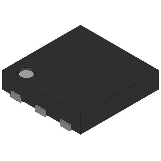
● Small Packages ··············································DFN(PLP)1820-6, SOT23-5
APPLICATIONS
● MP3 players, PDA, cellular phones
● Digital Still Cameras
● LCD Bias Supplies
● Portable blood pressure meter
● Wireless Handset
● GPS
1
�RP401x
BLOCK DIAGRAMS
Fixed output; RP401Kxx1A/B
VIN
VFM
CONTROL
STARTUP
CIRCUIT
OSCILLATOR
VREF
CURRENT
PROTECTION
LX
SWITCHING
CONTROL
PWM
E/A
SOFT
START
CURRENT
FEEDBACK
RAMP
COMPENSATION
CE
CHIP
ENABLE
VOUT
MODE CONTROL
MODE
GND
Adjustable output type: RP401K001C/D
VIN
VFM
CONTROL*
OSCILLATOR
VREF
PWM
STARTUP
CIRCUIT
CURRENT
PROTECTION
LX
SWITCHING
CONTROL
E/A
SOFT
START
RAMP
COMPENSATION
CE
CURRENT
FEEDBACK
CHIP
ENABLE
VOUT
VFB
GND
*) Applied to PWM/VFM automatic shift, RP401K001C only.
2
�RP401x
Fixed output type: RP401Nxx1C/D
VIN
VFM
CONTROL *
OSCILLATOR
VREF
PWM
STARTUP
CIRCUIT
CURRENT
PROTECTION
LX
SWITCHING
CONTROL
E/A
SOFT
START
CURRENT
FEEDBACK
RAMP
COMPENSATION
CE
CHIP
ENABLE
VOUT
GND
*) Applied to PWM/VFM automatic shift, RP401Nxx1C only.
SELECTION GUIDE
In the RP400 Series, output Voltage, Type of Output Voltage, and package for the ICs can be selected at the
user’s request.
Product Name
RP401Kxx1$-TR
RP401Nxx1$-TR-FE
Package
Quantity per Reel
Pb Free
Halogen Free
DFN (PLP)1820-6
5,000 pcs
Yes
Yes
SOT-23-5
3,000 pcs
Yes
Yes
xx: Designation of output voltage
00: Adjustable Version (1.8V ~ 5.5V) * recommendation range of output voltage / DFN(PLP)1820-6 only
xx: Fixed version: designation is possible in the range from 1.8V to 5.5V with a step of 0.1V
$: Designation of option.
A: with Mode pin, latch type over-current protection circuit
B: with Mode pin, without latch type over-current protection circuit
C: without Mode pin (PWM/VFM automatic shift)
D: without Mode pin (PWM-fix)
3
�RP401x
Product code table
Fixed
Latch type
over-current
protection
Yes
DFN(PLP)1820-6
Yes
Fixed
No
DFN(PLP)1820-6
C
No
(PWM/VFM automatic shift)
Fixed
No
SOT-23-5
Adjustable
No
DFN(PLP)1820-6
D
No
(PWM fix)
Fixed
No
SOT-23-5
Adjustable
No
DFN(PLP)1820-6
Version
MODE pin
Output Voltage
A
Yes
B
package
PIN CONFIGURATION
DFN(PLP)1820-6
SOT-23-5
5
6
1
5
2
4
3
4
1
(Bottom View)
2
3
(Top View)
PIN DESCRIPTION
RP401Kxx1A/B: DFN(PLP)1820-6
Pin No
Symbol
Pin Description
1
VIN
Power Supply Pin
2
CE
Chip Enable Pin (Active with ”H”)
3
GND
4
Lx
5
MODE
6
VOUT
Ground Pin
Internal NMOS Switch Drain Pin
Mode pin for switch over PWM-fix or PWM/VFM alternative
Output Pin
* Tab is GND level. (They are connected to the reverse side of this IC.) Connected to the GND is the recommendation,
leaving it open is also possible.
RP401K001C/D: DFN(PLP)1820-6
4
Pin No
Symbol
Pin Description
1
VIN
Power Supply Pin
2
CE
Chip Enable Pin (Active with ”H”)
3
GND
4
Lx
Internal NMOS Switch Drain Pin
5
VFB
Feedback input voltage for setting output voltage
6
VOUT
Output Pin
Ground Pin
�RP401x
* Tab is GND level. (They are connected to the reverse side of this IC.) Connected to the GND is the recommendation,
leaving it open is also possible.
RP401Nxx1C/D: SOT-23-5
Pin No
Symbol
1
CE
2
GND
3
VIN
4
VOUT
5
Lx
Pin Description
Chip Enable Pin (Active ”H”)
Ground Pin
Power Supply Pin
Output Pin
Internal NMOS Switch Drain Pin
ABSOLUTE MAXIMAM RATINGS
(GND=0V)
Symbol
Ratings
Unit
VIN Supply Voltage
-0.3 to 6.0
V
VOUT
VOUT Pin Voltage
-0.3 to 6.0
V
VLX
Lx Pin Input Voltage
-0.3 to 6.0
V
VCE
CE Pin Voltage
-0.3 to 6.0
V
VFB
VFB Pin Voltage
RP401K001C/D
-0.3 to 6.0
V
VMODE
MODE Pin Voltage
RP401K001A/B
-0.3 to 6.0
V
PD
Power Dissipation *
Ta
Ambient Temp Range
-40 to +85
°C
Tstg
Storage Temp Range
-55 to +125
°C
VIN
Items
SOT-23-5
420
DFN(PLP)1820-6
880
mW
* As for Power Dissipation, refer to PACKAGE INFORMATION.
ABSOLUTE MAXIMUM RATINGS
Electronic and mechanical stress momentarily exceeded absolute maximum ratings may cause the permanent damages
and may degrade the lifetime and safety for both device and system using the device in the field. The functional operation
at or over these absolute maximum ratings is not assured.
RECOMMENDED OPERATING CONDITIONS (ELECTRICAL CHARACTERISTICS)
All of electronic equipment should be designed that the mounted semiconductor devices operate within the
recommended operating conditions. The semiconductor devices cannot operate normally over the recommended operating
conditions, even if when they are used over such conditions by momentary electronic noise or surge. And the
semiconductor devices may receive serious damage when they continue to operate over the recommended operating
conditions.
5
�RP401x
ELECTRICAL CHARACTERISTICS
Adjustable types (RP401K001C/D)
Symbol
VIN
(Ta=25C)
Item
Conditions
TYP.
Input Voltage
MAX.
Unit
5.5
V
0.8
V
Vstart
Start-up Voltage
Load current =1mA
Vhold
Hold-on Voltage
Load current=1mA
IDD1
Quiescent Current 1
VIN=2V, VOUT=2.5V, VFB=0V
380
500
A
IDD2
Quiescent Current 2
(No switching)
001C
130
190
A
230
320
A
Standby Current
VIN=VOUT=5.5V, VCE=0V
0.15
3.00
A
Feedback Voltage
VIN=VOUT=3.3V
0.600
0.612
V
∆VOUT
/∆Ta
Output-Voltage
Temperature Coefficient
-40°C≤Ta≤85°C
Fosc
Switching Frequency
VIN=VOUT=3.3V, VFB=0V
∆fosc
/∆Ta
Switching Frequency
Temperature Coefficient
-40°C≤Ta≤85°C
±0.2
kHz
/°C
RONN
NMOS
On-Resistance (*1)
VOUT=3.3V
0.4
Ω
ICEH
CE ”H” Input Current
VIN=VOUT=VCE=5.5V
ICEL
CE ”L” Input Current
VIN=VOUT=5.5V, VCE=0V
IFBH
FB ”H” Input Current
VIN=VOUT=VFB=5.5V
IFBL
FB ”L” Input Current
VIN=VOUT=5.5V, VFB=0V
ILX
Lx Leakage Current
VIN=VOUT=VLX=5.5V, VCE=0V
ILxpeak
Lx Current limit (*2)
VIN=VSETx0.5V
VCEH
CE Input Voltage "H"
VCEL
CE Input Voltage "L"
Maxduty
Maximum Duty Cycle
VIN=VOUT=3.3V, VFB=0V
Soft start Time
VIN=1.65V, VOUT=3.3V, the time interval
from VCE changing from 0V to 1.5V edge
to VOUT being 2.97V
Istandby
VFB
tstart
001D
0.6
0.6
VIN=VOUT=5.5V, VFB=1.0V
0.588
V
ppm
/°C
±80
1020
1200
1380
0.2
0.2
2
80
A
A
A
-0.2
0.86
kHz
A
-0.2
1.00
A
A
0.7
*1) Guaranteed by design. NMOS On-Resistance depends on the VOUT voltage.
*2) Lx limit current changes according to the switching duty ratio.
6
MIN.
V
0.4
V
88
95
%
0.7
3.0
ms
�RP401x
Fixed output voltage types (RP401Kxx1A/B, RP401Nxx1C/D)
Symbol
VIN
Item
Conditions
Start-up Voltage
Load current =1mA
Vhold
Hold-on Voltage
Load current=1mA
IDD1
Quiescent Current 1
VIN=0.5xVSET, VOUT=0.95xVSET
IDD2
Quiescent Current 2
(No switching)
xx1A/B/C
Standby Current
VIN=VOUT=5.5V, VCE=0V
Output Voltage
VIN=VCE=1.5V
∆VOUT
/∆Ta
Output-Voltage
Temperature Coefficient
-40°C≤Ta≤85°C
Fosc
Switching Frequency
VIN=VOUT=3.3V, VFB=0V
∆fosc
/∆Ta
Switching Frequency
Temperature Coefficient
NMOS
On-Resistance (*1)
VOUT
RONN
TYP.
Input Voltage
Vstart
Istandby
(Ta=25C)
MIN.
xx1D
0.6
MAX.
Unit
5.5
V
0.8
V
0.6
VIN=VOUT=5.5V
V
VOUTx90
+130
VOUTx100
+250
A
130
190
A
230
320
A
0.15
3.00
A
x1.02
V
x0.98
ppm
/°C
±80
1020
1200
1380
kHz
-40°C≤Ta≤85°C
±0.2
kHz
/°C
VOUT=3.3V
0.4
Ω
ICEH
CE ”H” Input Current
VIN=VOUT=VCE=5.5V
ICEL
CE ”L” Input Current
VIN=VOUT=5.5V, VCE=0V
IMODEH
MODE ”H” Input Current
VIN=VOUT=VMODE=5.5V
IMODEL
MODE ”L” Input Current
VIN=VOUT=5.5V, VMODE=0V
ILX
Lx Leakage Current
VIN=VOUT=VLX=5.5V, VCE=0V
ILxpeak
Lx Current limit (*2)
VIN=VSETx0.5V
VCEH
CE Input Voltage "H"
VCEL
CE Input Voltage "L"
Maxduty
Maximum Duty Cycle
VIN=VOUT=0.95 x VSET
tstart
Soft start Time
tprot
Protection Delay Time
0.2
A
-0.2
0.2
A
A
-0.2
2
0.86
A
1.00
A
A
0.7
V
0.4
V
88
95
%
VIN=VSET x 0.5, the time interval from
VCE changing from 0V to 1.5V edge
to VOUT being VSET x 0.9
0.7
3.0
ms
VIN=VCE=3.3V
3.3
5.0
ms
80
*1) Guaranteed by design. NMOS On-Resistance depends on the VOUT voltage.
*2) Lx limit current changes according to the switching duty ratio.
*3) Applied to A/B version
*4) Applied to A version.
7
�RP401x
APPLICATION NOTES
Fixed Output Voltage Type (RP401Kxx1A/B)
L
4.7µH
Schottky Diode
VOUT
LX
VIN
CIN
10µF
RP401Kxx1x
CE
VOUT
CE Control
MODE Control
MODE
COUT
10µF×2
GND
Adjustable output type (RP401K001C/D)
L
4.7µH
Schottky Diode
VOUT
LX
VIN
C
10µF
IN
RP401K001x
CE
VOUT
CE Control
GND
COUT
10µF×2
R2
VFB
R1
8
�RP401x
Fixed output type (RP401Nxx1C/D)
L
4.7µH
Schottky Diode
VOUT
LX
VIN
CIN
10µF
CE Control
RP401Nxx1x
VOUT
CE
COUT
10µF×2
GND
External components
Capacitor CIN: C1608JB0J106M (TDK), COUT:
VOUT[V]
ILmax 0V
3.35
0
MODE Input Voltage[V]
3.30
3.25
1
0
O utput Voltage [V]
MODE Input Voltage
0V => 1.5V
3.35
MODE Input Voltage[V]
O utput Voltage [V]
1
3.30
3.25
Output Voltage
3.20
-5
-4
-3
-2
-1
0
1
Time [ms]
2
3
4
5
23
�POWER DISSIPATION
DFN(PLP)1820-6
Ver. A
The power dissipation of the package is dependent on PCB material, layout, and environmental conditions.
The following conditions are used in this measurement.
Measurement Conditions
Standard Test Land Pattern
Environment
Mounting on Board (Wind Velocity = 0 m/s)
Board Material
Glass Cloth Epoxy Plastic (Double-Sided Board)
Board Dimensions
40 mm × 40 mm × 1.6 mm
Top Side: Approx. 50%
Copper Ratio
Bottom Side: Approx. 50%
φ 0.54 mm × 30 pcs
Through-holes
Measurement Result
(Ta = 25°C, Tjmax = 125°C)
Standard Test Land Pattern
Power Dissipation
880 mW
Thermal Resistance
θja = (125 − 25°C) / 0.88 W = 114°C/W
40
1000
880
800
Standard Test Land Pattern
40
Power Dissipation PD (mW)
1200
600
400
200
0
0
25
50
75 85 100
125
Ambient Temperature (°C)
Power Dissipation vs. Ambient Temperature
150
IC Mount Area (mm)
Measurement Board Pattern
i
�PACKAGE DIMENSIONS
DFN(PLP)1820-6
Ver. A
1.6±0.1
A
1.80
0.20±0.1
B
5
4
6
0.25±0.1 0.25±0.1
X4
0.05
1.0±0.1
※
2.00
0.05 M AB
INDEX
S
0.05 S
0.05min
0.6MAX.
3
0.5
2
1
0.1NOM.
0.3±0.1
Bottom View
DFN(PLP)1820-6 Package Dimensions (Unit: mm)
*
∗ The tab on the bottom of the package is substrate level (GND). It is recommended that the tab be connected to the
ground plane on the board, or otherwise be left floating.
i
�1. The products and the product specifications described in this document are subject to change or discontinuation of
production without notice for reasons such as improvement. Therefore, before deciding to use the products, please
refer to Ricoh sales representatives for the latest information thereon.
2. The materials in this document may not be copied or otherwise reproduced in whole or in part without prior written
consent of Ricoh.
3. Please be sure to take any necessary formalities under relevant laws or regulations before exporting or otherwise
taking out of your country the products or the technical information described herein.
4. The technical information described in this document shows typical characteristics of and example application circuits
for the products. The release of such information is not to be construed as a warranty of or a grant of license under
Ricoh's or any third party's intellectual property rights or any other rights.
5. The products listed in this document are intended and designed for use as general electronic components in standard
applications (office equipment, telecommunication equipment, measuring instruments, consumer electronic products,
amusement equipment etc.). Those customers intending to use a product in an application requiring extreme quality
and reliability, for example, in a highly specific application where the failure or misoperation of the product could result
in human injury or death (aircraft, spacevehicle, nuclear reactor control system, traffic control system, automotive and
transportation equipment, combustion equipment, safety devices, life support system etc.) should first contact us.
6. We are making our continuous effort to improve the quality and reliability of our products, but semiconductor products
are likely to fail with certain probability. In order to prevent any injury to persons or damages to property resulting from
such failure, customers should be careful enough to incorporate safety measures in their design, such as redundancy
feature, fire containment feature and fail-safe feature. We do not assume any liability or responsibility for any loss or
damage arising from misuse or inappropriate use of the products.
7. Anti-radiation design is not implemented in the products described in this document.
8. The X-ray exposure can influence functions and characteristics of the products. Confirm the product functions and
characteristics in the evaluation stage.
9. WLCSP products should be used in light shielded environments. The light exposure can influence functions and
characteristics of the products under operation or storage.
10. There can be variation in the marking when different AOI (Automated Optical Inspection) equipment is used. In the
case of recognizing the marking characteristic with AOI, please contact Ricoh sales or our distributor before attempting
to use AOI.
11. Please contact Ricoh sales representatives should you have any questions or comments concerning the products or
the technical information.
Halogen Free
Ricoh is committed to reducing the environmental loading materials in electrical devices
with a view to contributing to the protection of human health and the environment.
Ricoh has been providing RoHS compliant products since April 1, 2006 and Halogen-free products since
April 1, 2012.
https://www.e-devices.ricoh.co.jp/en/
Sales & Support Offices
Ricoh Electronic Devices Co., Ltd.
Shin-Yokohama Office (International Sales)
2-3, Shin-Yokohama 3-chome, Kohoku-ku, Yokohama-shi, Kanagawa, 222-8530, Japan
Phone: +81-50-3814-7687 Fax: +81-45-474-0074
Ricoh Americas Holdings, Inc.
675 Campbell Technology Parkway, Suite 200 Campbell, CA 95008, U.S.A.
Phone: +1-408-610-3105
Ricoh Europe (Netherlands) B.V.
Semiconductor Support Centre
Prof. W.H. Keesomlaan 1, 1183 DJ Amstelveen, The Netherlands
Phone: +31-20-5474-309
Ricoh International B.V. - German Branch
Semiconductor Sales and Support Centre
Oberrather Strasse 6, 40472 Düsseldorf, Germany
Phone: +49-211-6546-0
Ricoh Electronic Devices Korea Co., Ltd.
3F, Haesung Bldg, 504, Teheran-ro, Gangnam-gu, Seoul, 135-725, Korea
Phone: +82-2-2135-5700 Fax: +82-2-2051-5713
Ricoh Electronic Devices Shanghai Co., Ltd.
Room 403, No.2 Building, No.690 Bibo Road, Pu Dong New District, Shanghai 201203,
People's Republic of China
Phone: +86-21-5027-3200 Fax: +86-21-5027-3299
Ricoh Electronic Devices Shanghai Co., Ltd.
Shenzhen Branch
1205, Block D(Jinlong Building), Kingkey 100, Hongbao Road, Luohu District,
Shenzhen, China
Phone: +86-755-8348-7600 Ext 225
Ricoh Electronic Devices Co., Ltd.
Taipei office
Room 109, 10F-1, No.51, Hengyang Rd., Taipei City, Taiwan (R.O.C.)
Phone: +886-2-2313-1621/1622 Fax: +886-2-2313-1623
�