RP402x Series
High Efficiency Small Packaged Step-up DC/DC Converter
No. EA-317-180912
OUTLINE
The RP402x is a high efficiency step-up DC/DC converter with synchronous rectifier. The device can start up
with low voltage of typically 0.7 V which is ideal for the applications powered by either one-cell or two-cell
alkaline, nickel-metal-hydride (NiMH) or one-cell Lithium-ion (Li+) batteries.
Internally, the RP402x consists of an oscillator, a reference voltage unit with soft start, a chip enable circuit, an
error amplifier, phase compensation circuits, a slope circuit, a PWM control circuit, a start-up circuit, a
PWM/VFM mode control circuit, internal switches and protection circuits.
The RP402x is employing synchronous rectification for improving the efficiency or rectification by replacing
diodes with built-in switching transistors. Using synchronous rectification not only increases circuit performance
but also allows a design to reduce parts count.
The RP402x is available in either internally fixed output voltage type or adjustable output voltage type. The
RP402xxxxx is the internally fixed output voltage type. The RP402x00xx is the adjustable output voltage type,
which allows output voltages that range from 1.8 V to 5.5 V via an external divider resistor.
The RP402x provides the forced PWM control and the PWM/VFM auto switching control. Either one of these
can be selected by inputting a signal to the MODE pin. The forced PWM control switches at fixed frequency
rate in low output current in order to reduce noise. Likewise, the PWM/VFM auto switching control automatically
switches from PWM mode to VFM mode in low output current in order to achieve high efficiency. The RP402N
is available in the PWM/VFM auto switching control. However, the RP402N is also available in the forced PWM
control as a custom-designed IC(1).
The RP402x has a soft-start time of typically 0.5 ms.
The RP402x features the complete output disconnect shutdown option and the input-to-output bypass
shutdown option. The RP402xxxxA/ B/ E/ F incorporates the complete output disconnect shutdown option,
which allows the output to be disconnected from the input. The RP402xxxxC/ D/ G/ H incorporates the inputto-output bypass shutdown option, which allows the output to be connected to the input.
The RP402x is protected against damage by a short-current protection, an over-voltage lockout, an over
voltage protection, an anti-ringing switch and a latch-type protection. An anti-ringing switch prevents the
occurrence of noise when an inductor current reaches a discontinuous mode. The RP402x provides optional
Latch function with current limit detection which can turn off the power in case the limit values are detected for
a fixed time and current limit circuit controls peak inductor currents in every clock. The latch-type protection
can be released by switching the CE pin from high to low while the power is turned on.
The RP402x is offered in a compact 5-pin SOT23-5 package or a 8-pin DFN(PLP)2020-8 package.
(1)
As for the custom-designed IC, please contact our sales representatives.
1
�RP402x
No. EA-317-180912
FEATURES
Low Voltage Start-up ·································· Typ. 0.7 V
Input Voltage Range ··································· Fixed Output Voltage Type: 0.6 V to 4.8 V
Adjustable Output Voltage Type: 0.6 V to 4.6 V
High Efficiency ·········································· 94% (100 mA/ 5.0 V, VIN = 3.6 V, 25°C)
90% (1 mA/ 5.0 V, VIN = 3.6 V, 25°C)
Output Current ·········································· 800 mA: VIN = 3.6 V, VOUT = 5.0 V
LX Driver ON Resistance ····························· NMOS/ PMOS: 0.20 Ω (VOUT = 5.0 V, 25°C)
PWM Oscillator Frequency ·························· 1.2 MHz (Normal PWM), 1.0 MHz (Forced PWM)
Output Voltage Range································· Fixed Output Voltage Type: 1.8 V to 5.5 V, 0.1 V step
Adjustable Output Voltage Type: 1.8 V to 5.5 V (recommended)
OVLO Detector Threshold ··························· Typ. 5.1 V
OVP Detector Threshold ····························· Typ. 6.0 V
LX Peak Current Limit ································· Typ. 1.5 A
Latch Protection Delay Time························· Typ. 3.3 ms (RP402Kxx1x, RP402Nxx1x)
Typ. 4.1 ms (RP402Kxx2x)
Soft-start Time ·········································· Typ. 0.5 ms
EMI Suppression (Built-in Anti-ringing Switch) (RP402Kxx1x, RP402Nxx1x)
Voltage Regulation at VIN > VOUT
Zero Input Complete Shutdown at VIN = 0 V
Input-to-Output Bypass Shutdown Option at CE = L (RP402xxxxC/ D/ G/ H)
Ceramic Capacitor Capable
Package ·················································· DFN(PLP)2020-8, SOT23-5
APPLICATIONS
MP3 Players, PDA
Digital Still Cameras
LCD Bias Supplies
Portable Blood Pressure Meter
Wireless Handset
GPS
USB-OTG
HDMI
2
�RP402x
No. EA-317-180912
SELECTION GUIDE
The package type, the set output voltage, the PWM control type, the shutdown option, the MODE pin option,
and the latch function are user-selectable options.
Selection Guide
Product Name
RP402Kxx#$-TR
RP402Nxx#$-TR-FE
Package
Quantity per Reel
Pb Free
Halogen Free
DFN(PLP)2020-8
5,000 pcs
Yes
Yes
SOT-23-5
3,000 pcs
Yes
Yes
xx: Specify the set output voltage (VSET).
00: Adjustable Output Voltage Type (1.8 V to 5.5 V, recommended voltage range)
xx: Fixed Output Voltage Type (1.8 V to 5.5 V, adjustable in 0.1 V step)
Please note: SOT-23-5 package is only available with fixed output voltage type.
#: Specify the PWM control type.
1: Normal PWM operation
2: Forced PWM operation
$: Specify the combination of the shutdown option, the MODE pin option and the latch function.
Version
Shutdown Options at CE = L
MODE Pin
Latch Function
A
Complete Output Disconnect
Yes
Yes
B
Complete Output Disconnect
Yes
No
C
Input-to-Output Bypass
Yes
Yes
D
Input-to-Output Bypass
Yes
No
E
Complete Output Disconnect
No
Yes
F
Complete Output Disconnect
No
No
G
Input-to-Output Bypass
No
Yes
H
Input-to-Output Bypass
No
No
Please refer to Selection Guide Table on the next page for detailed information.
3
�RP402x
No. EA-317-180912
Selection Guide Table
Package
Output
Voltage
Type
#$
Shutdown
Option
at CE = L
MODE Pin Function
MODE
Pin
1A
2A Complete
Output
Disconnect
1B
Fixed Output
Voltage Type
2B
1C
1D
Input-toOutput
Bypass
DFN(PLP)2020-8
Yes
1A
Adjustable
Output
Voltage
Type
2A Complete
Output
Disconnect
1B
2B
1C
1D
SOT-23-5
4
Fixed Output
Voltage Type
Input-toOutput
Bypass
1E Complete
Output
1F Disconnect
Power Controlling Method
“H”: Normal PWM Control,
“L”: PWM/VFM Auto Switching
Control
“H”: Forced PWM Control
Note: “H” recommended
“H”: Normal PWM Control,
“L”: PWM/VFM Auto Switching
Control
“H”: Forced PWM Control
Note: “H” recommended
“H”: Normal PWM Control,
“L”: PWM/VFM Auto Switching
Control
“H”: Normal PWM Control,
“L”: PWM/VFM Auto Switching
Control
“H”: Normal PWM Control,
“L”: PWM/VFM Auto Switching
Control
“H”: Forced PWM Control
Note: “H” recommended
“H”: Normal PWM Control,
“L”: PWM/VFM Auto Switching
Control
“H”: Forced PWM Control
Note: “H” recommended
“H”: Normal PWM Control,
“L”: PWM/VFM Auto Switching
Control
“H”: Normal PWM Control,
“L”: PWM/VFM Auto Switching
Control
PWM/VFM Auto Switching Control
PWM/VFM Auto Switching Control
No
1G Input-toOutput
1H Bypass
PWM/VFM Auto Switching Control
PWM/VFM Auto Switching Control
PWM
Latch
Controlling
Function
Method
Normal
PWM
Yes
Forced
PWM
Normal
PWM
No
Forced
PWM
Normal
PWM
Yes
Normal
PWM
No
Normal
PWM
Yes
Forced
PWM
Normal
PWM
No
Forced
PWM
Normal
PWM
Yes
Normal
PWM
No
Normal
PWM
Normal
PWM
Normal
PWM
Normal
PWM
Yes
No
Yes
No
�RP402x
No. EA-317-180912
BLOCK DIAGRAMS
*1
*2
This Bypass Switch is included in the RP402KxxxC / D only.
This Latch Timer is included in the RP402KxxxA / C only.
BYPASS
SW *1
OVER VOLTAGE
PROTECTION
V IN
Lx
REVERSE
DETECTOR
VFM
CONTROLLER
MODE
VREF
OSCILLATOR
POWER
CONTROLLER
STARTUP
CIRCUIT
+
PWM
CONTROLLER
-
VOUT
BACKGATE
CONTROLLER
SOFT
START
CE
CHIP
ENABLE
LATCH
TIMER*2
SWITCHING
CONTROLLER
CURRENT
PROTECTION
SHORT
PROTECTION
RAMP
COMPENSATION
+
CURRENT
FEEDBACK
GND
RP402Kxxxx Block Diagram
*1
*2
This Bypass Switch is included in the RP402KxxxC / D only.
This Latch Timer is included in the RP402KxxxA / C only.
BYPASS
SW *1
OVER VOLTAGE
PROTECTION
VIN
Lx
REVERSE
DETECTOR
VFM
CONTROLLER
MODE
VREF
POWER
CONTROLLER
STARTUP
CIRCUIT
+
PWM
CONTROLLER
-
VOUT
OSCILLATOR
BACKGATE
CONTROLLER
SOFT
START
CE
CHIP
ENABLE
LATCH
TIMER*2
SWITCHING
CONTROLLER
CURRENT
PROTECTION
SHORT
PROTECTION
RAMP
COMPENSATION
+
VFB
CURRENT
FEEDBACK
GND
RP402K00xx Block Diagram
5
�RP402x
No. EA-317-180912
*1
*2
This Bypass Switch is included in the RP402NxxxG/ H only.
This Latch Timer is included in the RP402NxxxE/ G only.
BYPASS
SW *1
OVER VOLTAGE
PROTECTION
V IN
Lx
REVERSE
DETECTOR
VFM
CONTROLLER
VREF
OSCILLATOR
POWER
CONTROLLER
STARTUP
CIRCUIT
+
PWM
CONTROLLER
-
V OUT
BACKGATE
CONTROLLER
SOFT
START
CE
CHIP
ENABLE
LATCH
TIMER*2
SWITCHING
CONTROLLER
CURRENT
PROTECTION
SHORT
PROTECTION
RAMP
COMPENSATION
+
CURRENT
FEEDBACK
GND
RP402Nxxxx Block Diagram
6
�RP402x
No. EA-317-180912
PIN DESCRIPTION
Top View
8
7
6
Bottom View
5
5
6
7
5
8
4
1
2
3
4
4
3
2
1
1
RP402K [DFN(PLP)2020-8] Pin Configurations
2
3
RP402N (SOT-23-5) Pin Configurations
The tab on the bottom of the package enhances thermal performance and is electrically connected to GND (substrate
level). It is recommended that the tab be connected to the ground plane on the board, or otherwise be left floating.
RP402Kxxxx Pin Description
Pin No.
Symbol
1
MODE
2
NC
3
GND
4
Lx
5
VOUT
6
VIN
7
NC
8
CE
Description
Mode Pin(1)
No Connection
Ground Pin
Internal NMOS Switch Drain Pin
Output Pin
Power Supply Pin
No Connection
Chip Enable Pin, Active-high
RP402K00xx Pin Description
Pin No.
Symbol
1
MODE
2
NC
3
GND
4
Lx
5
VOUT
6
VIN
7
VFB
8
CE
MODE Pin
No Connection
Ground Pin
Internal NMOS Switch Drain Pin
Output Pin
Power Supply Pin
Feedback Input Pin for Setting Output Voltage
Chip Enable Pin, Active-high
RP402Nxx1x Pin Description
Pin No.
Symbol
1
Lx
2
GND
3
CE
4
VIN
5
VOUT
Description
Internal NMOS Switch Drain Pin
Ground Pin
Chip Enable Pin, Active-high
Power Supply Pin
Output Pin
(1)
Description
(1)
MODE Pin = “H” is recommended for RP402Kxx2x.
7
�RP402x
No. EA-317-180912
ABSOLUTE MAXIMUM RATINGS
Absolute Maximum Ratings
Symbol
Rating
Unit
VIN Pin Voltage
−0.3 to 6.5
V
VOUT
VOUT Pin Voltage
−0.3 to 7.0
V
VLX
LX Pin Voltage
−0.3 to 6.5
V
VCE
CE Pin Voltage
−0.3 to 6.5
V
VFB
VFB Pin Voltage (RP402K00xx only)
−0.3 to 6.5
V
MODE Pin Voltage (RP402Kxxxx only)
−0.3 to 6.5
V
VIN
VMODE
PD
Parameter
Power Dissipation (1)
DFN(PLP)2020-8
1800
(JEDEC STD. 51-7)
SOT-23-5
660
mW
Tj
Junction Temperature Range
−40 to 125
°C
Tstg
Storage Temperature Range
−55 to 125
°C
ABSOLUTE MAXIMUM RATINGS
Electronic and mechanical stress momentarily exceeded absolute maximum ratings may cause the permanent
damages and may degrade the life time and safety for both device and system using the device in the field. The
functional operation at or over these absolute maximum ratings is not assured.
RECOMMENDED OPERATING CONDITIONS
Recommended Operating Conditions
Symbol
Parameter
Rating
Unit
VIN
Input Voltage
0.6 to 4.8
V
Ta
Operating Temperature
−40 to 85
°C
RECOMMENDED OPERATING CONDITIONS
All of electronic equipment should be designed that the mounted semiconductor devices operate within the
recommended operating conditions. The semiconductor devices cannot operate normally over the recommended
operating conditions, even if when they are used over such conditions by momentary electronic noise or surge. And
the semiconductor devices may receive serious damage when they continue to operate over the recommended
operating conditions.
(1)
8
Refer to POWER DISSIPATION for detailed information.
�RP402x
No. EA-317-180912
ELECTRICAL CHARACTERISTICS
The specifications surrounded by
are guaranteed by design engineering at −40°C ≤ Ta ≤ 85°C.
RP402xxxxx Electrical Characteristics (Not applicable to RP402K00xx)
Symbol
Parameter
Condition
VSTART
Start-up Voltage
RL = 5.5 kΩ
VHOLD
Hold-on Voltage after start-up(1)
RL = 5.5 kΩ
VOVLO
OVLO Voltage
-
VOVP
OVP Voltage
-
IDD1
Quiescent Current 1
IDD2
Quiescent Current 2(2)
Istandby
VOUT
ΔVOUT
/ΔTa
fosc
Min.
Typ.
0.7
(Ta = 25°C)
Max. Unit
0.8
V
0.6
5.1
V
6.0
V
VIN = VSET −0.4 V,
VOUT = 0.95 x VSET
1.6
mA
VIN = VSET −0.4 V,
VOUT = VSET + 0.2 V
21
37
RP402xxxxA/ B/ E/ F
VIN = 4.8 V, VOUT = 0V,
VCE = 0V
0.2
1.0
RP402xxxxC/ D/ G/ H
VIN = 4.8 V, VCE = 0 V
1.2
2.5
Standby Current
Output Voltage
VIN = VCE = 1.5 V
Output-Voltage
Temperature Coefficient
−40°C ≤ Ta ≤ 85°C
Switching
Frequency
RP402xxx1x
RP402xxx2x
VIN = 1.5 V,
VOUT = 0.95 x VSET
4.8
V
x0.985
x1.015
900
850
µA
V
ppm
/°C
50
1080
1020
µA
1200
1320
1380
1000
1100
1150
kHz
RONN
NMOS ON Resistance(1)
VOUT = 5.0 V
0.20
Ω
RONP
PMOS ON Resistance(1)
VOUT = 5.0 V
0.20
Ω
ICEH
CE ”H” Input Current
VIN = 4.8 V,
VOUT = VCE = 5 V
ICEL
CE ”L” Input Current
VIN = 4.8 V,
VOUT = 5 V, VCE = 0 V
RP402xxx1x
0.5
−0.5
µA
µA
VIN = 4.8V,
VCE = 0 V,
VMODE = 5.5 V
0.5
IMODEH
MODE ”H” Input
Current(3)
IMODEL
MODE ”L” Input Current(3)
VIN = 4.8 V, VCE = VMODE =
0V
ILXH
Lx ”H” Leakage Current
VIN = VOUT = VLX = 4.8V,
VCE = 0 V
0.5
µA
ILXL
Lx ”L”Leakage Current
VOUT = 5 V, VLX = 0 V,
VCE = 0 V
0.5
µA
ILXPEAK
RP402xxx2x
Lx Limit Current(4)
72
−0.5
1.3
µA
µA
1.5
A
All test items listed under ELECTRICAL CHARACTERISTICS are done under the pulse load condition (Tj ≈ Ta = 25°C).
(1)
Hold-on Voltage and NMOS/ PMOS ON Resistance are dependent on VOUT.
Quiescent Current 2 is not applicable to RP402xxx2x.
(3) MODE “H”/ “L” Input Current/ Voltage is only applicable to RP402Kxxxx.
(4) L Limit Current fluctuates depending on Duty.
X
(2)
9
�RP402x
No. EA-317-180912
ELECTRICAL CHARACTERISTICS (continued)
The specifications surrounded by
are guaranteed by design engineering at −40°C ≤ Ta ≤ 85°C.
RP402xxxxx Electrical Characteristics (Not applicable to RP402K00xx)
Symbol
Parameter
Condition
VCEH
CE ”H” Input Voltage
VCEL
CE “L” Input Voltage
(Ta = 25°C)
Min.
Typ.
Max.
0.7
V
0.3
(1)
VMODEH
MODE ”H” Input Voltage
VMODEL
MODE ”L” Input Voltage (1)
Unit
V
V
1.0
0.4
V
Oscillator Maximum Duty Cycle
VIN = 1.5 V, VOUT = 0.95
x VSET
80
88
95
%
tstart
Soft-start Time(2)
Measures the time when
VCE = 0 V to 1.5 V,
VOUT = VSET x 0.95
0.25
0.5
0.70
ms
tprot
Protection Delay Time(3)
RP402xxx1x
2.7
3.3
3.9
ms
RP402xxx2x
3.5
4.1
4.7
Maxduty
RONA
Anti-ringing Switch ON
RONB
Bypass Switch ON
Resistance(5)
IINZERO
VIN Zero Current
Resistance(4)
RP402xxxxC/ D/ G/ H
VIN = 2.5 V, VOUT = 3.3 V
100
Ω
VIN = 3.0 V,
VOUT = 0 V
160
Ω
VIN = 0 V, VOUT = 5.5 V
0.1
1.0
µA
All test items listed under ELECTRICAL CHARACTERISTICS are done under the pulse load condition (Tj ≈ Ta = 25°C).
(1) MODE
“H”/ “L” Input Current/ Voltage is only applicable to RP402Kxxxx.
VIN ≥ 1.7 V
(3) Protection Delay Time is not included in RP402xxxxB/ D/ F/ H.
(4) Anti-ringing Switch ON Resistance is dependent on V
OUT. Not applicable to RP402xxx2x.
(5) Bypass Switch ON Resistance is dependent on V .
IN
(2)
10
�RP402x
No. EA-317-180912
Electrical Characteristics by Differenct Output Voltage
VOUT (Ta = 25°C)
Product
Name
Min.
Typ.
Max.
RP402x18xx
1.773
1.800
1.827
RP402x19xx
1.872
1.900
1.929
RP402x20xx
1.970
2.000
2.030
RP402x21xx
2.069
2.100
2.132
RP402x22xx
2.167
2.200
2.233
RP402x23xx
2.266
2.300
2.335
RP402x24xx
2.364
2.400
2.436
RP402x25xx
2.463
2.500
2.538
RP402x26xx
2.561
2.600
2.639
RP402x27xx
2.660
2.700
2.741
RP402x28xx
2.758
2.800
2.842
RP402x29xx
2.857
2.900
2.944
RP402x30xx
2.955
3.000
3.045
RP402x31xx
3.054
3.100
3.147
RP402x32xx
3.152
3.200
3.248
RP402x33xx
3.251
3.300
3.350
RP402x34xx
3.349
3.400
3.451
RP402x35xx
3.448
3.500
3.553
RP402x36xx
3.546
3.600
3.654
RP402x37xx
3.645
3.700
3.756
RP402x38xx
3.743
3.800
3.857
RP402x39xx
3.842
3.900
3.959
RP402x40xx
3.940
4.000
4.060
RP402x41xx
4.039
4.100
4.162
RP402x42xx
4.137
4.200
4.263
RP402x43xx
4.236
4.300
4.365
RP402x44xx
4.334
4.400
4.466
RP402x45xx
4.433
4.500
4.568
RP402x46xx
4.531
4.600
4.669
RP402x47xx
4.630
4.700
4.771
RP402x48xx
4.728
4.800
4.872
RP402x49xx
4.827
4.900
4.974
RP402x50xx
4.925
5.000
5.075
RP402x51xx
5.024
5.100
5.177
RP402x52xx
5.122
5.200
5.278
RP402x53xx
5.221
5.300
5.380
RP402x54xx
5.319
5.400
5.481
RP402x55xx
5.417
5.500
5.582
11
�RP402x
No. EA-317-180912
ELECTRICAL CHARACTERISTICS (continued)
The specifications surrounded by
are guaranteed by design engineering at −40°C ≤ Ta ≤ 85°C.
RP402K00xx Electrical Characteristics
Symbol
VIN
Parameter
Condition
Start-up Voltage
RL = 5.5 kΩ
VHOLD
Hold-on Voltage after start-up(1)
RL = 5.5 kΩ
VOVLO
OVLO Voltage
VOVP
OVP Voltage
IDD1
Quiescent Current 1
IDD2
Quiescent Current 2(2)
VFB
Typ.
Input Voltage
VSTART
Istandby
Min.
Standby Current
4.6
V
0.8
V
V
0.6
5.1
V
6.0
V
VIN = 3 V, VOUT = 5 V,
VFB = 0.6 V
1.6
mA
VIN = 4.8 V, VOUT = 5.5 V,
VFB = 2.0 V, VMODE = 0 V
21
37
RP402KxxxA/ B
VIN = 4.8 V, VOUT = 0V,
VCE = 0V
0.2
1.0
RP402KxxxC/ D
VIN = 4.8 V, VCE = 0 V
1.2
2.5
1.00
1.015
4.6
Feedback Voltage
VIN = 3.0 V, VOUT = 5 V
ΔVFB
/ΔTa
Output Voltage Temperature
Coefficient
−40°C ≤ Ta ≤ 85°C
fosc
Switching
Frequency
RP402K001x
RP402K002x
RONN
NMOS ON Resistance(1)
RONP
Resistance(1)
PMOS ON
0.7
(Ta = 25°C)
Max.
Unit
VIN = 3.0 V, VOUT = 3.3 V,
VFB = 0.6 V
µA
V
ppm
/°C
50
1080
1020
1200
1320
1380
900
850
1000
1100
1150
kHz
VOUT = 5.0 V
0.20
Ω
VOUT = 5.0 V
0.20
Ω
ICEH
CE ”H” Input Current
VIN = 4.8 V, VOUT = VCE =
5.5 V
ICEL
CE ”L” Input Current
VIN = 4.8 V, VOUT = 5 V,
VCE = 0 V
RP402K001x
0.985
µA
0.5
−0.5
µA
µA
0.5
VIN = 4.8 V, VMODE = 5.5 V,
VCE = 0 V
IMODEH
MODE ”H” Input
Current
IMODEL
MODE ”H” Input Current
VIN = 4.8 V, VCE = VMODE =
0V
ILXH
Lx ”H” Leakage Current
VIN = VOUT = VLX = 4.8 V,
VCE = 0 V
0.5
µA
ILXL
Lx ”L”Leakage Current
VOUT = 5.0 V, VLX = 0 V,
VCE = 0 V
0.5
µA
ILXPEAK
RP402K002x
Lx Limit Current(3)
72
−0.5
1.3
µA
µA
1.5
A
All test items listed under ELECTRICAL CHARACTERISTICS are done under the pulse load condition (Tj ≈ Ta = 25°C).
(1)
Hold-on Voltage and NMOS/ PMOS ON Resistance are dependent on VOUT.
Quiescent Current 2 is not applicable to RP402K002x.
(3) L Limit Current fluctuates depending on Duty.
X
(2)
12
�RP402x
No. EA-317-180912
ELECTRICAL CHARACTERISTICS (continued)
The specifications surrounded by
are guaranteed by design engineering −40°C ≤ Ta ≤ 85°C.
RP402K00xx Electrical Characteristics
Symbol
Parameter
VCEH
CE ”H” Input Voltage
VCEL
CE ”L” Input Voltage
VMODEH
MODE ”H” Input Voltage
VMODEL
MODE ”L” Input Voltage
Maxduty
Condition
Min.
Typ.
(Ta = 25°C)
Max. Unit
0.7
V
0.3
V
1.0
Oscillator Maximum Duty Cycle
Time(1)
V
0.4
V
88
95
%
0.25
0.5
0.70
ms
VIN = 3.0 V, VOUT = 3.3 V,
VFB = 0.6 V
80
Measures the time when
VOUT = 3.3 V,
VCE = 0 V to 1.5 V,
VOUT = 3.13 V
tstart
Soft-start
tprot
Protection Delay
Time(2)
RONA
Anti-ringing Switch ON Resistance(3)
VIN = 2.5 V, VOUT = 3.3 V
100
Ω
RONB
Bypass Switch ON
Resistance(4)
VIN = 3.0 V,
VOUT = 0 V
160
Ω
VIN = 0 V, VOUT = 5.5 V
0.1
IINZERO
RP402K001x
-
2.7
3.3
3.9
ms
RP402K002x
-
3.5
4.1
4.7
ms
RP402KxxxC/ D
VIN Zero Current
1.0
µA
All test items listed under ELECTRICAL CHARACTERISTICS are done under the pulse load condition (Tj ≈ Ta = 25°C).
(1) Soft-start
Time is VIN ≥ 1.7 V.
Quiescent Current 2 is not applicable to RP402K002x.
(3) L Limit Current fluctuates depending on Duty.
X
(4) Bypass Switch ON Resistance is dependent on V
IN.
(2)
13
�RP402x
No. EA-317-180912
THEORY OF OPERATION
Forced PWM Control Type (RP402xx2A/ B)
While normal PWM control type prevents the reverse inductor current at light load, forced PWM control type
makes the inductor current reverse in order to eliminate the discontinuous current period. Therefore, even at
light load or when the voltage difference between input and output is less, forced PWM control type can
provide PWM operation without bursting.
Normal PWM
IL
x
Lx
Forced PWM
IL
x
Lx
Operating Waveform of Normal PWM/ Forced PWM Control Type
There is a case that forced PWM control performs burst operation without PWM operation because of the
conditions of use. The conditions which cause burst operation are various and differ in set output voltage, input
voltage, ambient temperature and load current.
Please note that forced PWM control type decreases the efficiency at light load and does not include antiringing switch. The graph below indicates the typical operational maximum input voltage of forced PWM control
type.
RP402Kxx1x: MODE = ”H” (Normal PWM), RP402Kxx2x: (Forced PWM)
RP402K33xx
1.8
3.5
1.6
3
1.4
1.2
1
0.8
0.6
0.4
RP402K181x
0.2
RP402K182x
0
2.5
2
1.5
1
RP402K331x
RP402K332x
0.5
0
1
14
( Ta = 25°C)
( Ta = 25°C)
Input Voltage @ PWM [V]
Input Voltage @ PWM [V]
RP402K18xx
10
Output Current IOUT [mA]
100
1
10
Output Current IOUT [mA]
100
�RP402x
No. EA-317-180912
RP402K50xx
RP402K55xx
( Ta = 25°C)
( Ta = 25°C)
5
6
4
Input Voltage @ PWM [V]
Input Voltage @ PWM [V]
4.5
3.5
3
2.5
2
1.5
RP402K501x
RP402K502x
1
0.5
5
4
3
2
RP402K551x
RP402K552x
1
0
0
1
10
Output Current IOUT [mA]
1
100
10
Output Current IOUT [mA]
100
MODE Pin (RP402K only)
When setting the MODE pin “high” of RP402K, it is recommended to connect the MODE pin “high” with the
VOUT pin to ensure stability. Please note that a current flows through the pull-down resistor to consume power
even in a standby state (CE=”low”) as the MODE pin is pulled down by an internal resistor when the Mode pin
“high” is connected with VIN pin. Since RP402Kxx2A/B have only Forced PWM control type, the MODE pin
“high” fixing is recommended to ensure safety, but also connecting the MODE pin to GND or using it in the
open state are other options.
Bypass Mode Application Example (RP402xxxxC/ D/ G/ H)
The RP402xxxxC/ D/ G/ H is available in bypass mode when CE = L. The shown below is the application
example of the device in bypass mode. In this application, when the main system is not in sleep, the
RP402xxxxC/ D/ G/ H is set to active state to supply power to the main system and RTC. When the main
system is in sleep, the RP 402xxxxC/ D/ G/ H is set to standby state to supply power to RTC in bypass mode.
Using the device in the bypass mode can reduce the power loss and the consumption of battery. Also, using
the device in bypass mode can eliminate external components for short-circuit protection.
L
C1
CE Control
LX
VIN
CE
RP402xxxx
C/ D/ G/ H
VOUT
MODE
GND
Main System
(VSET)
C2
VOUT
RTC
(A small amount of
current is required.)
15
�RP402x
No. EA-317-180912
Regulation Operation at VIN > VOUT
The RP402x regulates the output voltage to the set output voltage even when the input voltage is higher than
the set output voltage. Please note that this regulation operation decreases the efficiency and the maximum
output current driving ability. The maximum output current driving ability can be different due to the set output
voltage, the input voltage and the ambient temperature.
The following is the switching condition (Typ.) from step-up operation to the step-down regulation.
VIN ≤ VOUT−150 mV: Step-down regulation → Step-up operation
VIN > VOUT−100 mV: Step-up operation → Step-down regulation
Output Current vs.Input Voltage
RP402xxxxx
ILX vs.Input Voltage
RP402xxxxx
VOUT = 3.3V
500
600
450
550
400
500
350
300
ILX [mA]
Output Current IOUT [mA]
VOUT = 3.3V
250
200
150
450
400
350
300
100
250
50
200
0
3
3.5
4
4.5
5
3
3.5
4
4.5
5
5.5
Input Voltage VIN [V]
Input Voltage VIN [V]
Output Voltage Setting for RP402K00xx
The RP402K00xx can set the output voltage freely by the external divider resistors using the following equation.
Output Voltage = VFB (R1 + R2) / R2
(VFB = 1.0 V)
Zero Input Complete Shutdown at VIN = 0 V
The RP402x provides a zero input complete shutdown function that allows the device to shut down the output
when VIN = 0 V or VIN = open. This function protects against reverse current flow from VOUT to VIN when a
voltage is applied to the VOUT pin while VIN = 0 V or VIN = open.
Overcurrent Protection
The RP402x incorporates a LX peak current limit circuit as the overcurrent protection circuit which controls the
duty of LX when the LX peak current (ILXPEAK) reaches typically 1.5 A.
Latch Type Protection (RP402xxxxA/ C/ E/ G)
The RP402xxxxA/ C/ E/ G provides a latch type protection circuit to latch the power MOSFET to the off state
in order to stop the DC/DC operation. To release the latch type protection, switch the CE pin from high to low
once and switch it back to high while the power is turned on. Please note that the LX peak current (ILXPEAK) and
the protection delay time (tprot) are easily affected by the self-heating or heat radiation efficiency. The large
reduction in input voltage (VIN) or the unstable input voltage caused by short-circuit may affect the protection
operation or protection delay time.
16
�RP402x
No. EA-317-180912
Short-circuit Protection
The RP402x provides a short-circuit protection which stops the switching operation when a short circuit is
detected. After a consecutive fixed period of the short-circuit state, the device performs a restart with soft-start
operation. RP402xxxxA/ C/ E/ G latches the power in a stop state when the input voltage becomes lower than
typically 1.6V and it is short-circuited.
Overvoltage Protection
The RP402x provides an overvoltage lockout (OVLO) circuit for monitoring the input pin voltage and an
overvoltage protection (OVP) circuit for monitoring the output pin voltage. These circuits stops the switching
operation when an overvoltage is detected. If the output voltage is dropped below the set output voltage when
OVLO is released, the output voltage will be boosted to the set output voltage.
17
�RP402x
No. EA-317-180912
OUTPUT CURRENT AND SELECTION OF EXTERNAL COMPONENTS
Operation of Step-up DC/DC Converter and Output Current
Basic Circuit
Pch Tr.
Coil(L)
IOUT
VIN
VOUT
Nch Tr.
CL
GND
The inductor current (IL) flowing through the inductor (L)
Discontinuous Mode
Continuous Mode
IL max
IL
IL
IL max
IL min
IL min
tf
Iconst
t
ton
t =1/fosc
t
ton
toff
toff
t =1/fosc
A PWM control type step-up DC/DC converter has two operation modes characterized by the continuity of
inductor current: discontinuous current mode and continuous current mode.
The voltage applied to the inductor L, when transistor is ON, is described as “VIN”. So, the current is described
as “VIN x t / L”.
Therefore, the electric power (PON) supplied from the input side, while transistor is ON, is described as follows:
ton
PON VIN2 t/L dt ··························································································· Equation 1
0
18
�RP402x
No. EA-317-180912
In step-up circuit, power source supplies the electric power (POFF) even while transistor is OFF. The input
current supplied by power source while transistor is OFF is described as “(VOUT − VIN) x t / L”. Therefore, the
electric power POFF is described as follows:
POFF
tf
0
VIN (VOUT VIN) t/L dt ······································································· Equation 2
The time of which the inductance L releases the saved energy is described as “tf”. Therefore, the average
electric power (PAV) in a cycle is described as follows:
PAV 1/(ton toff) {
ton
0
VIN2 t/L dt
tf
0
VIN (VOUT VIN) t/L dt} ···················· Equation 3
In PWM control, when “tf = toff”, the inductor current becomes continuous, so the switching regulator operation
turns into continuous current mode. The current deviation between On time and Off time is equal under steadystate condition of continuous current mode as follows:
VIN x ton/ L = (VOUT − VIN) x toff / L ··············································································· Equation 4
The electric power (PAV) is equal to the output voltage (VOUTIOUT). Therefore, IOUT is as follows:
IOUT = fosc x VIN2 x ton2 / {2 x L (VOUT - VIN)} = VIN2 x ton / (2 x L x VOUT) ································ Equation 5
When IOUT becomes more than VIN ton toff / (2 L (ton + toff)), the inductor current becomes continuous,
so the switching regulator operation turns into continuous current mode. The continuous inductor current is
described as ICONST, so IOUT is described as follows:
IOUT = fosc x VIN2 x ton2 / (2 x L (VOUT − VIN)) + VIN x Iconst / VOUT ········································ Equation 6
The peak current (ILmax) flowing through the inductor is described as follows:
ILmax = Iconst + VIN x ton / L ····················································································· Equation 7
Put Equation 4 into Equation 6 to solve ILmax. ILmax is described as follows:
ILmax = VOUT / VIN x IOUT + VIN x ton / (2 x L) ·································································· Equation 8
However, ton = (1 − VIN / VOUT) / fosc. The peak current is more than IOUT.
Please consider ILmax when setting conditions of input and output, as well as selecting the external
components. The peak current in the discontinuous current mode in Equation 7 can be calculated by Iconst
= 0.
Please note: The above calculation formulas are based on the ideal operation of the device in continuous
mode. The loss caused by the external components and the built-in Lx switch are not included. Please use the
peak current in Equation 8 as a reference when selecting an inductor.
19
�RP402x
No. EA-317-180912
TIMING CHART
Soft-start Operation and Latch-type Protection Operation
Input
Voltage
CE
Voltage
Output
Current
1.60V (Typ.)
Output
Voltage
LX
Voltage
tprot
RP402xxx1x 3.3ms (Typ.)
RP402xxx2x 4.1ms (Typ.)
0.5ms (Typ.)
Standby
*1
*2
Low-Boost
Mode
Soft Start Period
VFM Mode*1
PWM Mode
LX-Peak
Current
Limit
Latch Protect*2
Only for RP402xxx1x (MODE = ”L”)
Only for RP402xxxxA/ C/ E/ G
< Start-up >
When CE is changed from ”L” to ”H”, DC/DC converter starts up the operation. The RP402x has Low-Boost
mode which can start up with low voltage such as 0.7 V. The DC/DC boosts up with Low-Boost mode until the
output voltage reaches to typically 1.6 V. When the output voltage becomes more than or equal to typically 1.6
V, the soft-start operation starts in order to control inrush current. The DC/DC boosts up the output voltage
until it reaches to the setting output voltage.
20
�RP402x
No. EA-317-180912
Please note: During Low-Boost mode, the oscillator frequency is dropped, so the step-up ability is low
compared to the normal operation mode. Please pay attention to the step-up ratio and the load current. Softstart time depends on “set output voltage”, “input voltage”, “ambient temperature”, and “load current”.
Soft Start Period vs.Input Voltage
RP402xxxxx
RL = 5.5kΩ
( Ta = 25°C )
100.0
Soft Start Period vs.Ta
RP402x33xx
1.0
VOUT = 3.3V
VIN = 1.8V
RL = 5.5kΩ
0.9
10.0
VSET=1.8V
VSET=3.3V
VSET=5.5V
1.0
Soft-start Time [ms]
Soft-start Time [ms]
0.8
0.7
0.6
0.5
0.4
0.3
0.2
0.1
0.1
0.0
0
1
2
3
Input Voltage VIN [V]
4
5
-50
-25
0
25
50
75
100
Ta [℃]
21
�RP402x
No. EA-317-180912
APPLICATION INFORMATION
L
C1
CE Control
MODE Control
LX
VIN
RP402Kxxxx
VOUT
CE
C2
VOUT
MODE
GND
RP402Kxxxx Typical Application (Fixed Output Voltage Type)
L
C1
CE Control
MODE Control
LX
VIN
RP402K00xx
VOUT
C2
CE
MODE
VOUT
RSPD
R1
CSPD
VFB
GND
R2
RP402K00xx Typical Application (Adjustable Output Voltage Type)
L
C1
CE Control
LX
VIN
RP402Nxx1x
CE
VOUT
C2
VOUT
GND
RP402Nxx1x Typical Application (Fixed Output Voltage Typ)
22
�RP402x
No. EA-317-180912
Recommended Components
Symbol
L
C1 (CIN)
Descriptions
VLF403215MT-2R2M, 2.2 µH, TDK
VLS3012HBX-2R2M, TDK
NRS5020T2R2NMGJ, TAIYO YUDEN
GRM188R60J106ME47, 10 µF, Murata
GRM188R60J106ME47, 10 µF x 2, Murata
C2 (COUT)
As for the fixed output voltage type (RP402x50xx), 10 µF x 1 can be used if the
mounting area is limited.
The speedup capacitor (CSPD) is required for the adjustable output voltage type.
Connect CSPD in parallel with the output resistor (R1).
To calculate the CSPD value, the following equation can be used:
f = 1 / (2 π × CSPD × R1)
CSPD
Adjust the CSPD value to make the oscillator frequency (f) approximately 20 kHz.
For example, VOUT = 5.0 V, R1 = 2 MΩ, R2 = 500 kΩ and CSPD = 4 pF.
The R1 and R2 values are calculated based on the operation efficiency under a light
load, therefore R1 and R2 are having high-resistance values. The feedback voltage
(VFB) can be affected by noise. To stabilize the device operation, decrease the R1 and
R2 values.
The speedup resistor (RSPD) is required for the adjustable output voltage type.
RSPD
Using RSPD can prevent the deterioration of the characteristics due to noise.
If there’s a possibility of generation of a spike noise, use an approximately 1 kΩ RSPD.
23
�RP402x
No. EA-317-180912
TECHNICAL NOTES
The performance of a power source circuit using this device is highly dependent on a peripheral circuit. A
peripheral component or the device mounted on PCB should not exceed its rated voltage, rated current or
rated power. When designing a peripheral circuit, please be fully aware of the following points. (Refer to PCB
Layout Considerations below.)
Ensure the VIN and GND lines are firmly connected. A large switching current flows through the GND lines
and the VIN line. If their impedance is too high, noise pickup or unstable operation may result. When the
built-in switch is turned off, the inductor may generate a spike-shaped high voltage. Use the highbreakdown voltage capacitor (COUT) which output voltage is 1.5 times or more than the set output voltage.
After a boosting of the step-up converter, the converter uses VOUT as a main power source. Therefore,
the ceramic capacitor between the VOUT pin and the GND pin acts as a bypass capacitor. Considering the
bias dependence, place a 10 µF or more ceramic capacitor (COUT) between the VOUT pin - the GND pin as
close as possible. Also, place an approximately 10 µF ceramic capacitor (CIN) between the VIN pin - the
GND pin.
Use a 2.2 µH inductor (L) which is having a low equivalent series resistance, having enough tolerable
current and which is less likely to cause magnetic saturation.
The MODE pin is controlled with a logic voltage. To make it "H", 1.0 V or more must be forced to the
MODE pin. If power supply is less than 1.0 V, MODE pin must be pulled up to VOUT.
When using Forced PWM Control Type, the MODE pin should be “H”.
The RP402x can reset the latch protection circuit by setting the CE signal ‘L’ (VCE < 0.3 V) once while the
power is switched on (VIN > 0.8 V). If setting the CE pin when VIN does not reach 0.8 V due to too large
CIN, the latch protection circuit cannot be reset correctly. Likewise, if starting the device up when the CE
pin is shorted to the VIN pin or VOUT pin, the latch protection circuit cannot be reset.
If controlling the CE pin by input voltage, the gradient of the power supply at rising must be considered.
So, the CE pin must be connected via the delay circuit or the voltage detector to become the CE pin
voltage less than 0.3 V until the VIN becomes more than 0.8V.
Placing a snubber circuit (Serial connection of CR) in parallel with a diode can reduce the spike noise
caused by the Lx pin. The conditions of circuit board has a strong influence on the CR time constant and
the efficiency of the converter. The evaluation has to be done using an actual converter (10 Ω and 300
pF).
24
�RP402x
No. EA-317-180912
PCB Layout Considerations
Current Path on PCB
Figure 1 and Figure 2 show the current pathways of application circuits when MOSFET is turned ON or when
MOSFET is turned OFF, respectively. As shown in Figure 1 and Figure 2, the currents flow in the directions of
blue or green arrows. The parasitic components (impedance, inductance or capacitance) formed in the
pathways indicated by the red arrows affect the stability of the system and become the cause of noise. Reduce
the parasitic components as much as possible. The current pathways should be made by short and thick
wirings.
Figure 1. MOSFET-ON
Figure 2. MOSFET-OFF
25
�RP402x
No. EA-317-180912
RP402Kxxxx (PKG: DFN(PLP)2020-8pin) Typical Board Layout
Top Layer
Bottom Layer
RP402K00xx (PKG: DFN(PLP)2020-8pin) Typical Board Layout
Top Layer
Bottom Layer
RP402Nxxxx (PKG: SOT-23-5pin) Typical Board Layout
Top Layer
26
Bottom Layer
�RP402x
No. EA-317-180912
TYPICAL CHARACTERISTICS
Note: Typical Characteristics are intended to be used as reference data; they are not guaranteed.
1) Output Voltage vs. Output Current
RP402x181x
MODE = "L" ( VFM / PWM )
1.9
RP402K181x
MODE = "H" ( Normal PWM )
(Ta = 25°C)
Input Voltage
1.9
1.84
0.8V
1.82
1.8
1.0V
1.78
1.2V
1.76
1.74
1.84
0.8V
1.82
1.8
1.0V
1.78
1.2V
1.76
1.5V
1.72
1.7
1.7
0.1
1
10
100
1000
Output Current IOUT(mA)
RP402K182x
( Forced PWM )
1.9
10000
0.1
1
10
100
1000
Output Current IOUT(mA)
10000
(Ta = 25°C)
Input Voltage
1.88
Output Voltage VOUT (V)
0.7V
1.86
1.74
1.5V
1.72
(Ta = 25°C)
Input Voltage
1.88
0.7V
1.86
Output Voltage VOUT (V)
Output Voltage VOUT (V)
1.88
0.7V
1.86
1.84
0.8V
1.82
1.8
1.0V
1.78
1.2V
1.76
1.74
1.5V
1.72
1.7
0.1
1
10
100
1000
Output Current IOUT(mA)
RP402x331x
MODE = "L" ( VFM / PWM )
3.5
10000
0.8V
3.35
1.2V
1.5V
3.3
1.8V
3.25
2.0V
3.2
Output Voltage VOUT (V)
3.4
Input Voltage
0.7V
3.4
0.8V
3.35
1.2V
3.3
1.5V
1.8V
3.25
2.5V
3.2
3.0V
3.15
3.1
(Ta = 25°C)
3.45
0.7V
3.15
2.0V
2.5V
3.0V
3.1
0.1
1
10
100
1000
Output Current IOUT(mA)
RP402K332x
( Forced PWM )
3.5
Output Voltage VOUT (V)
3.5
Input Voltage
3.45
Output Voltage VOUT (V)
RP402K331x
MODE = "H" ( Normal PWM )
(Ta = 25°C)
10000
0.1
1
10
100
1000
Output Current IOUT(mA)
10000
(Ta = 25°C)
Input Voltage
3.45
0.7V
3.4
0.8V
3.35
1.2V
1.5V
3.3
1.8V
3.25
2.0V
3.2
2.5V
3.15
3.0V
3.1
0.1
1
10
100
1000
Output Current IOUT(mA)
10000
27
�RP402x
No. EA-317-180912
RP402x501x
MODE = "L" ( VFM / PWM )
RP402K501x
MODE = "H" ( Normal PWM )
(Ta = 25°C)
5.2
Input Voltage
5.15
0.8V
5.1
1.2V
5.05
1.8V
2.4V
5
2.7V
4.95
3.2V
4.9
Output Voltage VOUT (V)
Output Voltage VOUT (V)
5.2
3.7V
4.85
Input Voltage
5.15
0.8V
5.1
1.2V
5.05
1.8V
2.4V
5
2.7V
4.95
3.2V
4.9
3.7V
4.85
4.2V
4.8
4.2V
4.8
0.1
1
10
100
1000
Output Current IOUT(mA)
RP402K502x
( Forced PWM )
5.2
Output Voltage VOUT (V)
(Ta = 25°C)
10000
0.1
1
10
100
1000
Output Current IOUT(mA)
10000
(Ta = 25°C)
Input Voltage
5.15
0.8V
5.1
1.2V
5.05
1.8V
2.4V
5
2.7V
4.95
3.2V
4.9
3.7V
4.85
4.2V
4.8
0.1
1
10
100
1000
Output Current IOUT(mA)
RP402x551x
MODE = "L" ( VFM / PWM )
(Ta = 25°C)
0.8V
5.7
1.2V
1.8V
5.6
2.4V
5.5
2.7V
3.2V
5.4
3.7V
4.2V
5.3
4.8V
0.1
1
10
100
1000
Output Current IOUT(mA)
RP402K552x
( Forced PWM )
5.8
Output Voltage VOUT (V)
Input Voltage
0.8V
5.7
1.2V
1.8V
5.6
2.4V
5.5
2.7V
3.2V
5.4
3.7V
4.2V
5.3
4.8V
5.2
5.2
0.1
10000
(Ta = 25°C)
Input Voltage
0.8V
5.7
1.2V
5.6
1.8V
2.4V
5.5
2.7V
3.2V
5.4
3.7V
4.2V
5.3
4.8V
5.2
0.1
28
RP402K551x
MODE = "H" ( Nomal PWM )
(Ta = 25°C)
5.8
Input Voltage
Output Voltage VOUT (V)
Output Voltage VOUT (V)
5.8
10000
1
10
100
1000
Output Current IOUT(mA)
10000
1
10
100
1000
Output Current IOUT(mA)
10000
�RP402x
No. EA-317-180912
Efficiency vs. Output Current
RP402x181x
MODE = "L" ( VFM / PWM )
100
RP402K181x
MODE = "H" ( Normal PWM )
(Ta = 25°C)
100
Input Voltage
0.7V
70
0.8V
60
50
1.0V
40
0.8V
60
50
1.0V
40
1.2V
20
20
1.5V
10
0
0.01
0.7V
70
30
1.2V
30
Input Voltage
80
Efficiency η(%)
Efficiency η(%)
80
(Ta = 25°C)
90
90
0.1
1
10
100
Output Current IOUT(mA)
RP402K182x
( Forced PWM )
100
1.5V
10
0
0.01
1000
0.1
1
10
100
Output Current IOUT(mA)
1000
(Ta = 25°C)
Input Voltage
90
0.7V
Efficiency η(%)
80
70
60
0.8V
50
40
1.0V
30
20
1.2V
10
0.1
1
10
100
Output Current IOUT(mA)
RP402x331x
MODE = "L" ( VFM / PWM )
100
1000
100
Input Voltage
90
0.8V
70
1.2V
60
1.5V
50
(Ta = 25°C)
Input Voltage
90
0.7V
80
Efficiency η(%)
RP402K331x
MODE = "H" ( Normal PWM )
(Ta = 25°C)
0.7V
80
Efficiency η(%)
0
0.01
0.8V
70
1.2V
60
1.5V
50
40
1.8V
40
1.8V
30
2.0V
30
2.0V
20
2.5V
20
2.5V
10
3.0V
10
3.0V
0
0.01
0.1
1
10
100
Output Current IOUT(mA)
RP402K332x
( Forced PWM )
100
0
0.01
1000
1
10
100
Output Current IOUT(mA)
1000
Input Voltage
0.7V
80
0.8V
70
60
1.2V
50
1.5V
40
1.8V
30
20
2.0V
10
2.5V
0
0.01
0.1
(Ta = 25°C)
90
Efficiency η(%)
2)
0.1
1
10
100
Output Current IOUT(mA)
1000
29
�RP402x
No. EA-317-180912
RP402x501x
MODE = "L" ( VFM / PWM )
100
2.4V
50
40
2.7V
30
1.2V
70
1.8V
60
2.4V
50
2.7V
3.2V
30
3.2V
20
3.7V
20
3.7V
10
4.2V
10
0.1
1
10
100
Output Current IOUT(mA)
RP402K502x
( Forced PWM )
100
0
0.01
1000
1
10
100
Output Current IOUT(mA)
1000
Input Voltage
0.8V
80
1.2V
70
1.8V
60
2.4V
50
40
2.7V
30
3.2V
20
3.7V
10
4.2V
0
0.01
4.2V
0.1
(Ta = 25°C)
90
Efficiency η(%)
0.8V
40
0
0.01
0.1
1
10
100
Output Current IOUT(mA)
RP402x551x
MODE = "L" ( VFM / PWM )
100
1000
RP402K551x
MODE = "H" ( Normal PWM )
(Ta = 25°C)
100
Input Voltage
(Ta = 25°C)
Input Voltage
0.8V
90
0.8V
80
1.2V
80
1.2V
70
1.8V
70
1.8V
60
2.4V
60
2.4V
50
2.7V
50
2.7V
40
3.2V
40
3.2V
30
3.7V
30
3.7V
20
4.2V
20
4.2V
10
4.8V
10
4.8V
90
Efficiency η(%)
Efficiency η(%)
60
0
0.01
0.1
1
10
100
Output Current IOUT(mA)
RP402K552x
( Forced PWM )
100
(Ta = 25°C)
Input Voltage
0.8V
80
1.2V
70
1.8V
60
2.4V
50
2.7V
40
3.2V
30
3.7V
20
4.2V
10
0
0.01
0
0.01
1000
90
0.1
1
10
100
Output Current IOUT(mA)
1000
Efficiency η(%)
Efficiency η(%)
1.8V
Input Voltage
80
1.2V
70
(Ta = 25°C)
90
0.8V
80
Efficiency η(%)
100
Input Voltage
90
30
RP402K501x
MODE = "H" ( Normal PWM )
(Ta = 25°C)
0.1
1
10
100
Output Current IOUT(mA)
1000
�RP402x
No. EA-317-180912
3)
Standby Current vs. Ambient Temperature
RP402x33xA/B/E/F
RP402x33xC/D/G/H
VIN = 4.8V / VOUT = OPEN
5.0
4.5
4.5
4.0
4.0
Standby Current [µA]
Standby Current [µA]
VIN = 4.8V / VOUT = GND
5.0
3.5
3.0
2.5
2.0
1.5
3.0
2.5
2.0
1.5
1.0
1.0
0.5
0.5
0.0
0.0
-50
-25
0
25
50
75
-50
100
-25
0
25
50
75
100
Ta [°C]
Ta [°C]
4)
3.5
Supply Current 1 vs. Ambient Temperature
RP402x33xx
VIN = VSET - 0.4V / VOUT = 0.95 × VSET
5.0
4.5
4.0
IDD1 [mA]
3.5
3.0
2.5
2.0
1.5
1.0
0.5
0.0
-50
-25
0
25
50
75
100
Ta [°C]
5)
Supply Current 2 vs. Ambient Temperature
RP402x331x
VIN = VSET - 0.4V / VOUT = VSET + 0.2V
30
25
IDD2 [µA]
20
15
10
5
0
-50
-25
0
25
50
75
100
Ta [°C]
Start-up vs. Ambient Temperature
RP402x33xx
( RL = 5.5kΩ )
0.8
Start-up Voltage [V]
6)
0.75
0.7
0.65
0.6
-50
-25
0
25
50
75
100
Ta [°C]
31
�RP402x
No. EA-317-180912
7)
Hold-on Voltage vs. Ambient Temperature
RP402x33xx
( RL = 5.5kΩ )
0.41
Hold-on Voltage [V]
0.39
0.37
0.35
0.33
0.31
0.29
0.27
0.25
-50
-25
0
25
50
75
100
Ta [°C]
8)
Oscillator Frequency vs. Ambient Temperature
RP402K331x
MODE = "H" ( Normal PWM )
VIN = 1.5V
1400
1200
1350
1150
1100
1250
fosc [Hz]
fosc [Hz]
1300
1200
1150
850
800
-25
0
25
50
75
100
RP402x33xx
100
90
80
Max duty [%]
70
60
50
40
30
20
10
0
-50
-25
0
25
50
75
100
Ta [°C]
10) Lx Current Limit vs. Duty
RP402xxxxx
(Ta = 25°C)
2500
2300
RP402K001x (5.0V)
2100
RP402K001x (3.3V)
1900
RP402K001x (2.9V)
1700
RP402K001x (2.5V)
1500
RP402K001x (2.3V)
1300
RP402K001x (2.0V)
1100
RP402K001x (1.8V)
900
700
500
30
40
50
60
70
-50
-25
0
25
Ta [°C]
Maxduty vs. Ambient Temperature
Lxpeak [mA]
950
900
Ta [°C]
80
90
Duty [%]
11) Lx Current Limit vs. Ambient Temperature
32
1000
1050
-50
20
1050
1100
1000
9)
RP402K332x
( Forced PWM )
VIN = 1.5V
50
75
100
�RP402x
No. EA-317-180912
RP402x33xx
VIN = 1.65V
2500
2300
2100
Lxpeak [mA]
1900
1700
1500
1300
1100
900
700
500
-50
-25
0
25
50
75
100
Ta [°C]
12) CE ”H” Input Voltage vs. Ambient Temperature
RP402xxxxx
0.8
0.7
VCEH [V]
0.6
0.5
0.4
0.3
0.2
-50
-25
0
25
50
75
100
Ta [°C]
13) MODE ”H” Input Voltage vs. Ambient Temperature
RP402Kxxxx
1.0
VMODEH [V]
0.8
0.6
0.4
0.2
0.0
-50
-25
0
25
50
75
100
Ta [°C]
14) Output Voltage vs. Ambient Temperature
RP402x33xx
VIN = 1.5V
3.40
Output Voltage VOUT [V]
3.38
3.36
3.34
3.32
3.30
3.28
3.26
3.24
3.22
3.20
-50
-25
0
25
50
75
100
Ta [°C]
33
�RP402x
No. EA-317-180912
15) Feedback Voltage vs. Ambient Temperature
RP402K00xx (VSET = 5.0V)
VIN = 3.0V
1.03
Feedback Voltage VFB [V]
1.02
1.01
1.00
0.99
0.98
0.97
-50
-25
0
25
50
75
100
Ta [°C]
16) Start-up Waveform (COUT = 20 μF)
RP402K331A
RP402K331A
(Ta = 25°C)
VIN = 1.2V / IOUT = 1mA)
Output Voltage
4
3
1.5
1
0.5
CE Input Voltage
2
Output Voltage VOUT /
CE Input Voltage [V]
0
Inductor Current ILX [A]
Output Voltage VOUT /
CE Input Voltage [V]
1
Inductor Current
Output Voltage
3
CE Input Voltage
2
(Ta = 25°C)
VIN = 1.8V / IOUT = 1mA)
1
0
1.5
1
Inductor Current
0.5
0
0
-0.5
-0.5
0
0.5
1
1.5
2
2.5
3
3.5
4
Inductor Current ILX [A]
4
-0.5
4.5
-0.5
0
0.5
Time t [ms]
1
1.5
2
Time t [ms]
17) Load Transient Response (COUT = 20 μF)
RP402x181x
MODE = "L" (VFM / PWM)
VIN = 0.9V
1.7
Output Current
1mA 50mA
50
20
40 60 80
Time t [μs]
1.7
Output Current
50mA 1mA
50
0
(Ta = 25°C)
0
0.5
VIN = 0.9V
1
1.5
2
2.5
Time t [ms]
3
3.5
RP402K181x
MODE = "H" (Normal PWM)
4
4.5
(Ta = 25°C)
1.9
Output Voltage
1.7
Output Current
1mA 50mA
50
-40
-20
0
20
40 60 80
Time t [μs]
0
100 120 140 160
Output Voltage VOUT [V]
1.75
Output Current IOUT [mA]
1.85
1.8
Output Voltage
1.8
1.75
1.7
Output Current
50mA 1mA
50
0
-0.5
0
0.5
1
1.5
2
2.5
Time t [ms]
3
3.5
4
4.5
Output Current IOUT [mA]
1.85
Output Voltage VOUT [V]
1.75
-0.5
1.9
34
1.8
0
100 120 140 160
RP402K181x
MODE = "H" (Normal PWM)
VIN = 0.9V
Output Voltage VOUT [V]
1.75
0
Output Voltage
1.85
1.8
Output Current IOUT [mA]
Output Voltage VOUT [V]
1.85
-20
(Ta = 25°C)
1.9
Output Voltage
-40
RP402x181x
MODE = "L" (VFM / PWM)
Output Current IOUT [mA]
1.9
VIN = 0.9V
(Ta = 25°C)
�RP402x
No. EA-317-180912
RP402K182x
(Forced PWM)
VIN = 0.9V
Output Current
1mA 50mA
50
0
20
40 60 80
Time t [μs]
Output Current
50mA 1mA
50
-40
(Ta = 25°C)
-20
0
20
40 60 80
Time t [ms]
0
100 120 140 160
RP402x331x
MODE = "L" (VFM / PWM)
VIN = 1.8V
(Ta = 25°C)
3.2
3.1
Output Current
1mA 200mA
200
-20
0
20
40 60 80
Time t [μs]
0
100 120 140 160
RP402K331x
MODE = "H" (Normal PWM)
VIN = 1.8V
Output Voltage
3.4
3.3
3.2
3.1
Output Current
200mA 1mA
200
Output Current IOUT [mA]
3.3
Output Voltage VOUT [V]
3.5
Output Voltage
3.4
-40
0
-0.5
(Ta = 25°C)
0
0.5
1
1.5
2
2.5
Time t [ms]
3
3.5
4
RP402K331x
MODE = "H" (Normal PWM)
VIN = 1.8V
3.6
4.5
(Ta = 25°C)
Output Current IOUT [mA]
3.3
3.2
3.1
Output Current
1mA 200mA
200
-40
-20
0
20
40 60 80
Time t [μs]
RP402K332x
(Forced PWM)
VIN = 1.8V
Output Voltage VOUT [V]
3.5
Output Voltage
3.4
0
100 120 140 160
Output Voltage
3.4
3.3
3.2
3.1
Output Current
200mA 1mA
200
Output Current IOUT [mA]
3.6
3.5
0
-0.5
(Ta = 25°C)
0
0.5
1
1.5
2
2.5
Time t [ms]
RP402K332x
(Forced PWM)
VIN = 1.8V
3
3.5
4
4.5
(Ta = 25°C)
3.6
3.6
3.5
3.3
3.2
3.1
Output Current
1mA 200mA
200
-40
-20
0
20
40 60 80
Time t [μs]
0
100 120 140 160
Output Current IOUT [mA]
Output Voltage
3.4
Output Voltage VOUT [V]
3.5
Output Voltage
3.4
3.3
3.2
3.1
Output Current
200mA 1mA
200
-40
-20
0
20
40 60 80
Time t [ms]
Output Current IOUT [mA]
Output Voltage VOUT [V]
1.7
3.6
3.5
Output Voltage VOUT [V]
1.75
0
100 120 140 160
RP402x331x
MODE = "L" (VFM / PWM)
VIN = 1.8V
Output Voltage
1.8
Output Current IOUT [mA]
1.7
Output Voltage VOUT [V]
Output Current IOUT [mA]
1.75
3.6
Output Voltage VOUT [V]
1.85
Output Voltage
1.8
Output Current IOUT [mA]
Output Voltage VOUT [V]
1.85
-20
(Ta = 25°C)
1.9
1.9
-40
RP402K182x
(Forced PWM)
VIN = 0.9V
(Ta = 25°C)
0
100 120 140 160
35
�RP402x
No. EA-317-180912
Output Current
1mA 250mA
250
RP402K501x
MODE = "H" (Normal PWM)
VIN = 3.7V
(Ta = 25°C)
4.9
4.85
Output Current
1mA 250mA
250
RP402K502x
(Forced PWM)
VIN = 3.7V
250
0
0.5
1
1.5
2
2.5
Time t [ms]
3
3.5
4
RP402K501x
MODE = "H" (Normal PWM)
VIN = 3.7V
4.5
(Ta = 25°C)
5.1
Output Voltage
5.05
5
4.95
4.9
Output Current
250mA 1mA
4.85
250
0
100 120 140 160
40 60 80
Time t [μs]
Output Current
250mA 1mA
0
-0.5
0
0.5
1
3
3.5
4
RP402K502x
(Forced PWM)
VIN = 3.7V
(Ta = 25°C)
1.5
2
2.5
Time t [ms]
4.5
(Ta = 25°C)
5.2
5.15
5.05
Output Voltage
5
4.95
4.9
4.85
Output Current
1mA 250mA
250
-40
-20
0
20
40 60 80
Time t [μs]
0
100 120 140 160
Output Voltage
5.1
5.05
5
4.95
4.9
Output Current
250mA 1mA
4.85
250
-40
-20
0
20
40 60 80
Time t [μs]
Output Current IOUT [mA]
5.1
20
4.9
4.85
5.15
4.95
0
5
4.95
5.2
Output Voltage
-20
5.05
0
5
-40
Output Voltage
-0.5
Output Voltage VOUT [V]
Output Voltage VOUT [V]
5.05
(Ta = 25°C)
5.1
0
100 120 140 160
40 60 80
Time t [μs]
Output Voltage VOUT [V]
20
Output Current IOUT [mA]
5.1
0
Output Voltage VOUT [V]
4.85
Output Current IOUT [mA]
4.9
Output Current IOUT [mA]
Output Voltage VOUT [V]
4.95
-20
RP402K501x
MODE = "L" (VFM / PWM)
5.15
5
-40
VIN = 3.7V
5.2
Output Voltage
5.05
Output Voltage VOUT [V]
(Ta = 25°C)
Output Current IOUT [mA]
5.1
RP402K501x
MODE = "L" (VFM / PWM)
Output Current IOUT [mA]
VIN = 3.7V
0
100 120 140 160
18) Output Voltage Waveform (COUT = 20 μF)
3.34
Output Voltage
3.35
3.3
LX Voltage
3.25
4
2
0
Output Voltage VOUT [V]
VIN = 1.5V / IOUT = 1mA
LX Voltage VLX [V]
Output Voltage VOUT [V]
3.4
RP402x331x
MODE = "L" (VFM / PWM )
(Ta = 25°C)
VIN = 1.5V / IOUT = 100mA
(Ta = 25°C)
Output Voltage
3.32
3.3
LX Voltage
3.28
4
2
0
-2
-2
0
1
2
3
Time t [ms]
36
4
5
0
1
2
Time t [μs]
3
4
5
LX Voltage VLX [V]
RP402x331x
MODE = "L" (VFM / PWM )
�RP402x
No. EA-317-180912
RP402K331x
MODE = "H" (Normal PWM )
3.34
Output Voltage
3.35
3.3
LX Voltage
3.25
4
2
Output Voltage VOUT [V]
VIN = 1.5V / IOUT = 1mA
(Ta = 25°C)
LX Voltage VLX [V]
VIN = 1.5V / IOUT = 100mA
(Ta = 25°C)
Output Voltage
3.32
3.3
LX Voltage
3.28
4
2
0
0
-2
-2
0
1
2
3
4
0
5
1
RP402K332x
(Forced PWM )
4
RP402K332x
(Forced PWM )
(Ta = 25°C)
3.34
VIN = 1.5V / IOUT = 1mA
VIN = 1.5V / IOUT = 100mA
3.3
LX Voltage
3.25
4
2
0
Output Voltage VOUT [V]
Output Voltage
3.35
LX Voltage VLX [V]
Output Voltage VOUT [V]
3
5
Time t [μs]
Time t [μs]
3.4
2
(Ta = 25°C)
Output Voltage
3.32
3.3
LX Voltage
3.28
4
2
0
-2
0
1
2
3
4
LX Voltage VLX [V]
Output Voltage VOUT [V]
3.4
LX Voltage VLX [V]
RP402K331x
MODE = "H" (Normal PWM )
-2
5
0
Time t [μs]
1
2
3
4
5
Time t [μs]
19) Mode Switching Waveform
RP402K331x
( Ta = 25°C )
VIN = 1.5V / IOUT = 1mA
Output Voltage VOUT [V]
2
0
MODE Input Voltage
3.4
3.35
3.3
MODE Input Voltage [V]
4
Output Voltage
3.25
3.2
-2
-1
0
1
2
3
4
Time t [ms]
5
6
7
8
20) Bypass Switch ON Resistance
RP402xxxxC/D/G/H
300.0
(Ta= 25°C)
Vin=2
V
250.0
Vin=3.
2V
RONB [Ω]
200.0
150.0
100.0
50.0
0.0
0
2
4
6
VOUT [V]
37
�RP402x
No. EA-317-180912
21) PWM Operable Maximum Input Voltage vs. Ambient Temperature
RP402Kxx2x: (Forced PWM)
RP402Kxx1x: MODE = "H" (Normal PWM)
RP402K50xx
RP402K50xx
( IOUT = 10mA)
( IOUT = 1mA)
5
5
4.5
4.5
Input Voltage @ PWM [V]
Input Voltage @ PWM [V]
4
3.5
3
2.5
2
1.5
1
RP402K502x
RP402K501x
0.5
4
3.5
3
2.5
2
1.5
1
RP402K502x
RP402K501x
0.5
0
0
-50
-25
0
25
Ta [°C]
50
75
100
-50
-25
0
25
Ta [°C]
50
75
100
75
100
RP402K50xx
( IOUT = 100mA)
5
Input Voltage @ PWM [V]
4.5
4
3.5
3
2.5
2
1.5
1
RP402K502x
0.5
RP402K501x
0
-50
-25
0
25
Ta [°C]
50
75
100
22) Reverse Current at VIN = 0 vs. Ambient Temperature
RP402xxxxx
VIN = 0V / VOUT = 5.5V
0.2
0.0
IINZERO [µA]
-0.2
-0.4
-0.6
-0.8
-1.0
-50
-25
0
25
50
75
100
Ta [°C]
23) Latch Protection Delay Time vs. Ambient Temperature
RP402xxx2A/C/E/G
RP402xxx1A/C/E/G
VIN = 4.5V
4.0
4.8
3.8
4.6
3.6
4.4
tPROT [ms]
tPROT [ms]
VIN = 4.5V
3.4
4.0
3.0
3.8
3.6
2.8
-50
-25
0
25
Ta [°C]
38
4.2
3.2
50
75
100
-50
-25
0
25
Ta [°C]
50
�POWER DISSIPATION
DFN(PLP)2020-8
Ver. A
The power dissipation of the package is dependent on PCB material, layout, and environmental conditions.
The following measurement conditions are based on JEDEC STD. 51-7.
Measurement Conditions
Item
Measurement Conditions
Environment
Mounting on Board (Wind Velocity = 0 m/s)
Board Material
Glass Cloth Epoxy Plastic (Four-Layer Board)
Board Dimensions
76.2 mm × 114.3 mm × 0.8 mm
Copper Ratio
Outer Layer (First Layer): Less than 95% of 50 mm Square
Inner Layers (Second and Third Layers): Approx. 100% of 50 mm Square
Outer Layer (Fourth Layer): Approx. 100% of 50 mm Square
Through-holes
0.3 mm × 23 pcs
Measurement Result
(Ta = 25°C, Tjmax = 125°C)
Item
Measurement Result
Power Dissipation
1800 mW
Thermal Resistance (ja)
ja = 53°C/W
Thermal Characterization Parameter (ψjt)
ψjt = 27°C/W
ja: Junction-to-Ambient Thermal Resistance
ψjt: Junction-to-Top Thermal Characterization Parameter
2000
1800
1800
Power Dissipation (mW)
1600
1400
1200
1000
800
600
400
200
0
0
25
50
75 85
Ambient Temperature (°C)
100
125
Power Dissipation vs. Ambient Temperature
Measurement Board Pattern
i
�PACKAGE DIMENSIONS
DFN (PLP) 2020-8
Ver. B
*
*
DFN (PLP) 2020-8 Package Dimensions
∗ The tab on the bottom of the package shown by blue circle is a substrate potential (GND). It is recommended that this
tab be connected to the ground plane on the board but it is possible to leave the tab floating.
i
�POWER DISSIPATION
SOT-23-5
Ver. A
The power dissipation of the package is dependent on PCB material, layout, and environmental conditions.
The following measurement conditions are based on JEDEC STD. 51-7.
Measurement Conditions
Item
Measurement Conditions
Environment
Mounting on Board (Wind Velocity = 0 m/s)
Board Material
Glass Cloth Epoxy Plastic (Four-Layer Board)
Board Dimensions
76.2 mm × 114.3 mm × 0.8 mm
Copper Ratio
Outer Layer (First Layer): Less than 95% of 50 mm Square
Inner Layers (Second and Third Layers): Approx. 100% of 50 mm Square
Outer Layer (Fourth Layer): Approx. 100% of 50 mm Square
Through-holes
0.3 mm × 7 pcs
Measurement Result
Item
(Ta = 25°C, Tjmax = 125°C)
Measurement Result
Power Dissipation
660 mW
Thermal Resistance (ja)
ja = 150°C/W
Thermal Characterization Parameter (ψjt)
ψjt = 51°C/W
ja: Junction-to-Ambient Thermal Resistance
ψjt: Junction-to-Top Thermal Characterization Parameter
Power Dissipation vs. Ambient Temperature
Measurement Board Pattern
i
�SOT-23-5
PACKAGE DIMENSIONS
Ver. A
2.9±0.2
1.1±0.1
1.9±0.2
0.8±0.1
(0.95)
4
1
2
0~0.1
0.2min.
+0.2
1.6-0.1
5
2.8±0.3
(0.95)
3
0.4±0.1
+0.1
0.15-0.05
SOT-23-5 Package Dimensions
i
�1. The products and the product specifications described in this document are subject to change or discontinuation of
production without notice for reasons such as improvement. Therefore, before deciding to use the products, please
refer to Ricoh sales representatives for the latest information thereon.
2. The materials in this document may not be copied or otherwise reproduced in whole or in part without prior written
consent of Ricoh.
3. Please be sure to take any necessary formalities under relevant laws or regulations before exporting or otherwise
taking out of your country the products or the technical information described herein.
4. The technical information described in this document shows typical characteristics of and example application circuits
for the products. The release of such information is not to be construed as a warranty of or a grant of license under
Ricoh's or any third party's intellectual property rights or any other rights.
5. The products listed in this document are intended and designed for use as general electronic components in standard
applications (office equipment, telecommunication equipment, measuring instruments, consumer electronic products,
amusement equipment etc.). Those customers intending to use a product in an application requiring extreme quality
and reliability, for example, in a highly specific application where the failure or misoperation of the product could result
in human injury or death (aircraft, spacevehicle, nuclear reactor control system, traffic control system, automotive and
transportation equipment, combustion equipment, safety devices, life support system etc.) should first contact us.
6. We are making our continuous effort to improve the quality and reliability of our products, but semiconductor products
are likely to fail with certain probability. In order to prevent any injury to persons or damages to property resulting from
such failure, customers should be careful enough to incorporate safety measures in their design, such as redundancy
feature, fire containment feature and fail-safe feature. We do not assume any liability or responsibility for any loss or
damage arising from misuse or inappropriate use of the products.
7. Anti-radiation design is not implemented in the products described in this document.
8. The X-ray exposure can influence functions and characteristics of the products. Confirm the product functions and
characteristics in the evaluation stage.
9. WLCSP products should be used in light shielded environments. The light exposure can influence functions and
characteristics of the products under operation or storage.
10. There can be variation in the marking when different AOI (Automated Optical Inspection) equipment is used. In the
case of recognizing the marking characteristic with AOI, please contact Ricoh sales or our distributor before attempting
to use AOI.
11. Please contact Ricoh sales representatives should you have any questions or comments concerning the products or
the technical information.
Halogen Free
Ricoh is committed to reducing the environmental loading materials in electrical devices
with a view to contributing to the protection of human health and the environment.
Ricoh has been providing RoHS compliant products since April 1, 2006 and Halogen-free products since
April 1, 2012.
https://www.e-devices.ricoh.co.jp/en/
Sales & Support Offices
Ricoh Electronic Devices Co., Ltd.
Shin-Yokohama Office (International Sales)
2-3, Shin-Yokohama 3-chome, Kohoku-ku, Yokohama-shi, Kanagawa, 222-8530, Japan
Phone: +81-50-3814-7687 Fax: +81-45-474-0074
Ricoh Americas Holdings, Inc.
675 Campbell Technology Parkway, Suite 200 Campbell, CA 95008, U.S.A.
Phone: +1-408-610-3105
Ricoh Europe (Netherlands) B.V.
Semiconductor Support Centre
Prof. W.H. Keesomlaan 1, 1183 DJ Amstelveen, The Netherlands
Phone: +31-20-5474-309
Ricoh International B.V. - German Branch
Semiconductor Sales and Support Centre
Oberrather Strasse 6, 40472 Düsseldorf, Germany
Phone: +49-211-6546-0
Ricoh Electronic Devices Korea Co., Ltd.
3F, Haesung Bldg, 504, Teheran-ro, Gangnam-gu, Seoul, 135-725, Korea
Phone: +82-2-2135-5700 Fax: +82-2-2051-5713
Ricoh Electronic Devices Shanghai Co., Ltd.
Room 403, No.2 Building, No.690 Bibo Road, Pu Dong New District, Shanghai 201203,
People's Republic of China
Phone: +86-21-5027-3200 Fax: +86-21-5027-3299
Ricoh Electronic Devices Shanghai Co., Ltd.
Shenzhen Branch
1205, Block D(Jinlong Building), Kingkey 100, Hongbao Road, Luohu District,
Shenzhen, China
Phone: +86-755-8348-7600 Ext 225
Ricoh Electronic Devices Co., Ltd.
Taipei office
Room 109, 10F-1, No.51, Hengyang Rd., Taipei City, Taiwan
Phone: +886-2-2313-1621/1622 Fax: +886-2-2313-1623
�
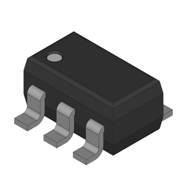


 工商网监
湘ICP备2023018690号
工商网监
湘ICP备2023018690号
