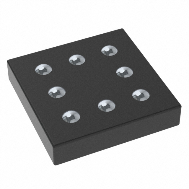
RP517x Series
0.3 V Ultra-low Output Voltage 300 mA Buck DC/DC Converter
No.EA-519-200304
OVERVIEW
RP517x is a low-voltage resistance buck DC/DC converter featuring ultra-low 0.3 μA quiescent current and
0.3 V output voltage. Suitable for wearable and IoT devices which require long-life batteries and downsizing.
KEY BENEFITS
● Ultra-low consumption current (I Q : 0.3 μA) with the VFM control for DC/DC (switching frequency: 1 MHz max.)
● Suitable for low power devices due to its ultra-low output voltage range from 0.3 V to 1.2 V
● Suitable for coin batteries and USB ports due to its wide input range from 1.8 V to 5.5 V
● Selectable 3 packages: WLCSP, DFN and SOT. Suitable for IC cards due to WLCSP’s thickness of 0.4 mm and
less.
KEY SPECIFICATIONS
•
•
Output current: 300 mA
Output Voltage Range: 0.3 V to 1.2 V
(Settable in 0.1 V step)
Output Voltage Accuracy: ±18 mV
Built-in Driver On-resistance (V IN = 3.6 V):
Typ. PMOS 0.15 Ω, NMOS 0.15 Ω (RP517Z)
Standby Current: 0.01 µA
•
•
•
TYPICAL APPLICATIONS
TYPICAL PERFORMANCE CHARACTERISTICS
RP517x051x, Ta=25°C
SELECTION GUIDE
VIN
VOUT
VIN
LX
VOUT
CIN
10 µF
Product Name
L
2.2 µH
RP517x
COUT
RP517Zxx1$-TR-F
Package
Quantity per Reel
WLCSP-8-P1
5,000 pcs
DFN(PLP)2527-10
5,000 pcs
SOT-89-5
1,000 pcs
22 µF
CE
RP517Kxx1$-TR
GND
RP517Hxx1$-T1-FE
xx: The set output voltage (V SET )
Fixed Output Voltage Type:
0.3 V (03) to 1.2 V (12) in 0.1 V step
PACKAGES (unit: mm)
$: The auto-discharge option
Version Auto-discharge Function
WLCSP-8-P1
DFN(PLP)2527-10
SOT-89-5
1.45 x 1.48 x 0.36
2.7 x 2.5 x 0.6
4.5 x 4.35 x 1.5
C
D
No
Yes
V SET
0.3 V to 1.2 V
APPLICATIONS
•
•
•
•
Wearable equipment such as SmartWatch, SmartBand and Health monitoring
Li-ion battery-used equipment, Coin cell-used equipment
Low power RF such as Bluetooth® Low Energy, Zigbee, WiSun and ANT
Low power CPU, Memory, Sensor device and Energy harvester
1
�RP517x
No.EA-519-200304
SELECTION GUIDE
The set output voltage, the auto-discharge function( 1) and the packages are user-selectable options.
Selection Guide
Product Name
RP517Zxx1$-TR-F
RP517Kxx1$-TR
RP517Hxx1$-T1-FE
Package
Quantity per Reel
Pb Free
Halogen Free
WLCSP−8−P1
5,000 pcs
Yes
Yes
DFN(PLP)2527-10
5,000 pcs
Yes
Yes
SOT-89-5
1,000 pcs
Yes
Yes
xx: Specify the set output voltage (V SET )
Fixed Output Voltage Type (2): 0.3 V (03) to 1.2 V (12) in 0.1 V step
$: Select the auto-discharge option
(1)
Version
Auto-discharge Function
C
No
D
Yes
V SET
0.3 V to 1.2 V
Auto-discharge function quickly lowers the output voltage to 0 V by releasing the electrical charge accumulated in the
external capacitor, when the chip enable signal is switched from the active mode to the standby mode.
(2) The custom specification of 0.05 V step is available.
2
�RP517x
No.EA-519-200304
BLOCK DIAGRAMS
High Side
Current
Detector
VOUT
VIN
-
Soft Start
+
Switching
Control
LX
Vref
CE
Enable
Control
Low Side
Current
Detector
UVLO
GND
RP517xxx1C Block Diagram
High Side
Current
Detector
VOUT
VIN
-
Soft Start
+
Switching
Control
LX
Vref
CE
Enable
Control
UVLO
Low Side
Current
Detector
GND
RP517xxx1D Block Diagram
3
�RP517x
No.EA-519-200304
PIN DESCRIPTIONS
Top View
Bottom View
3
3
2
2
1
1
A
B
C
C
B
A
RP517Z (WLCSP-8-P1) Pin Configuration
9
8
7
6
6
7
8
9
4
5
Bottom View
Top View
10
10
(1)
1
2
3
4
5
5
4
3
2
1
1
RP517K [DFN(PLP)2527-10] Pin Configuration
1
2
3
RP517H (SOT-89-5)
Pin Configuration
RP517Z (WLCSP-8-P1) Pin Descriptions
Pin No.
Symbol
A1
VIN
Input Pin
B1
VIN
Input Pin
C1
LX
Switching Pin
A2
VOUT
Output Pin
C2
GND
Ground Pin
A3
CE
B3
GND
Ground Pin
C3
GND
Ground Pin
(1) The
Description
Chip Enable Pin (Active-high)
tab on the bottom of the package enhances thermal performance and is electrically connected to GND (substrate
level). It is recommended that the tab be connected to the ground plane on the board, or otherwise be left floating.
4
�RP517x
No.EA-519-200304
RP517K [DFN(PLP)2527-10] Pin Descriptions
Pin No.
Symbol
Description
1
VOUT
Output Pin
2
GND
Ground Pin
3
GND
Ground Pin
4
LX
Switching Pin
5
LX
Switching Pin
6
VIN
Input Pin
7
VIN
Input Pin
8
NC
No connection
9
CE
Chip Enable Pin (Active-high)
10
NC
No connection
RP517H (SOT-89-5) Pin Descriptions
Pin No.
Symbol
Description
1
VOUT
Output Pin
2
GND
Ground Pin
3
LX
Switching Pin
4
VIN
Input Pin
5
CE
Chip Enable Pin (Active-high)
5
�RP517x
No.EA-519-200304
ABSOLUTE MAXIMUM RATINGS
Absolute Maximum Ratings
Symbol
Parameter
Rating
Unit
−0.3 to 6.5
V
V IN
Input Pin Voltage
V LX
LX Pin Voltage
−0.3 to V IN + 0.3
V
V CE
CE Pin Voltage
−0.3 to 6.5
V
V OUT
VOUT Pin Voltage
−0.3 to 6.5
V
WLCSP-8-P1, JEDEC STD. 51
840
mW
DFN(PLP)2527-10, JEDEC STD. 51
2500
mW
SOT-89-5, JEDEC STD. 51
2600
mW
PD
Power Dissipation(1)
Tj
Junction Temperature Range
−40 to 125
°C
Tstg
Storage Temperature Range
−55 to 125
°C
ABSOLUTE MAXIMUM RATINGS
Electronic and mechanical stress momentarily exceeded absolute maximum ratings may cause permanent damage
and may degrade the lifetime and safety for both device and system using the device in the field. The functional
operation at or over these absolute maximum ratings is not assured.
RECOMMENDED OPERATING CONDITIONS
Recommended Operating Conditions
Symbol
Parameter
Rating
Unit
V IN
Input Voltage
1.8 to 5.5
V
Ta
Operating Temperature Range
−40 to 85
°C
RECOMMENDED OPERATING CONDITIONS
All of electronic equipment should be designed that the mounted semiconductor devices operate within the
recommended operating conditions. The semiconductor devices cannot operate normally over the recommended
operating conditions, even if they are used over such conditions by momentary electronic noise or surge. And the
semiconductor devices may receive serious damage when they continue to operate over the recommended operating
conditions.
(1)
6
Refer to POWER DISSIPATION for detailed information.
�RP517x
No.EA-519-200304
ELECTRICAL CHARACTERISTICS
are guaranteed by design engineering at −40°C ≤ Ta ≤ 85°C.
The specifications surrounded by
RP517x Electrical Characteristics
Symbol
V OUT
(Ta = 25°C)
Parameter
Condition
Output Voltage
V IN = V CE = 3.6 V
Operating Quiescent Current
V IN = V CE = V OUT = 5.5 V,
V SET = 0.6 V, at rest
Standby Current
V IN = 5.5 V, V CE = 0 V
I CEH
CE Pin Input Current, high
V IN = V CE = 5.5 V
I CEL
CE Pin Input Current, low
IQ
I STANDBY
I VOUTH
I VOUTL
R DISN
VOUT pin input current,
high
VOUT pin input current,
low
Auto-discharge NMOS
On-state Resistance (1)
+0.018
V
µA
0.3
−0.025
0
0.025
µA
V IN = 5.5 V, V CE = 0 V
−0.025
0
0.025
µA
V IN = V OUT = 5.5 V, V CE = 0 V
−0.025
0
0.025
µA
V IN = 5.5 V, V CE = V OUT = 0 V
−0.025
0
0.025
µA
V IN = 3.6 V, V CE = 0 V
V CEL
CE Pin Input Voltage, low
1.8 V ≤ V IN ≤ 5.5 V
NMOS on-resistance
Unit
µA
1.8 V ≤ V IN ≤ 5.5 V
R ONN
−0.018
Max.
0.5
CE Pin Input Voltage, high
PMOS on-resistance
Typ.
0.01
V CEH
R ONP
Min.
Ω
60
1.0
V
0.4
V
RP517Z
V IN = 3.6 V, I LX = −100 mA
0.15
Ω
RP517K
V IN = 3.6 V, I LX = −100 mA
0.19
Ω
RP517H
V IN = 3.6 V, I LX = −100 mA
0.19
Ω
RP517Z
V IN = 3.6 V, I LX = −100 mA
0.15
Ω
RP517K
V IN = 3.6 V, I LX = −100 mA
0.19
Ω
RP517H
V IN = 3.6 V, I LX = −100 mA
0.19
Ω
10
ms
mA
t START
Soft-start time
V IN = V CE = 3.6 V
I LXLIM
LX current limit
V IN = V CE = 3.6 V
300
580
V IN = V CE , falling
1.40
1.50
1.65
V
V IN = V CE , rising
1.55
1.65
1.80
V
V UVLOF
V UVLOR
Undervoltage lockout
(UVLO) threshold voltage
All test items listed under Electrical Characteristics are done under the pulse load condition (Tj ≈ Ta = 25°C).
Test circuit is operated with “Open Loop Control” (GND = 0 V), unless otherwise specified.
(1)
RP517xxx1D only
7
�RP517x
No.EA-519-200304
Product-specific Electrical Characteristics
RP517xxx1x
Min.
V OUT [V]
Typ.
RP517x031x
0.282
0.30
0.318
RP517x041x
0.382
0.40
0.418
RP517x051x
0.482
0.50
0.518
RP517x061x
0.582
0.60
0.618
RP517x071x
0.682
0.70
0.718
RP517x081x
0.782
0.80
0.818
RP517x091x
0.882
0.90
0.918
RP517x101x
0.982
1.00
1.018
RP517x111x
1.082
1.10
1.118
RP517x121x
1.182
1.20
1.218
Product name
8
(Ta = 25°C)
Max.
�RP517x
No.EA-519-200304
TYPICAL APPLICATION CIRCUIT
VIN
VOUT
VIN
LX
L
2.2 µH
RP517x
VOUT
CIN
10 µF
COUT
22 µF
CE
GND
RP517x Typical Application Circuit
Precautions for Selecting External Components
・Using ceramic capacitors with low ESR (Equivalent Series Resistance) are recommended. Select capacitors
with bias characteristics and input/output voltages taken into consideration.
・When a built-in Lx switch is turned off, a spike-like high voltage may be generated due to an inductor. C OUT
voltage resistance should be 1.5 times or more than the set output voltage.
・Select an inductor having small DC resistance, sufficient allowable current and less possibility of causing
magnetic saturation.
9
�RP517x
No.EA-519-200304
TECHNICAL NOTES
The performance of a power source circuit using this device is highly dependent on the peripheral circuit. A
peripheral component or the device mounted on PCB should not exceed a rated voltage, a rated current or a
rated power. When designing a peripheral circuit, please be fully aware of the following points.
・When an intermediate voltage other than VIN and GND is input to the CE pin, a supply current may be
increased by a through current of a logic circuit in the IC. The CE pin is neither pulled up nor pulled down,
therefore the operation is not stable at open.
10
�RP517x
No.EA-519-200304
THEORY OF OPERATION
Soft-start Time
Starting-up with CE Pin
The IC starts to operate when the CE pin voltage (V CE ) exceeds the threshold voltage. The threshold voltage
is preset between CE “High” input voltage (V CEH ) and CE “Low” input voltage (V CEL ). After the start-up of the
IC, soft-start circuit starts to operate. Then, after a certain period of time, the reference voltage (V REF ) in the
IC gradually increases up to the specified value. Switching starts when V REF reaches the preset voltage, and
after that the output voltage rises as V REF increases. Soft-start time (t START ) indicates the period from the time
soft-start circuit gets activated to the time V REF reaches the specified voltage. t START is not always equal to the
turn-on speed of the DC/DC converter. Note that the turn-on speed could be affected by the power supply
capacity, the output current (I OUT ), the inductance and the output capacitor value (C OUT ).
VCEH
Threshold Level
CE Pin Input Voltage
VCEL
Soft-start Time
(VCE)
IC Internal Reference Voltage
(VREF)
Lx Voltage
Soft-start Circuit
operation starts.
(VLX)
Output Voltage
(VOUT)
Depending on Power Supply,
Load Current, External Components
Timing Chart: Starting-up with CE Pin
Starting-up with Power Supply
After the power-on, when V IN exceeds the UVLO release voltage (V UVLOR ), the IC starts to operate. Then, softstart circuit starts to operate and after a certain period of time, V REF gradually increases up to the specified
value. Switching starts when V REF reaches the preset voltage, and after that the output voltage rises as V REF
increases. The turn-on speed of V OUT could be affected by following conditions:
1. The V IN turn-on speed determined by the power supply to the IC and the C IN
2. The output capacitor value (C OUT ) and the output current (I OUT )
Input Voltage
VSET
VUVLOR
VUVLOF
(VIN)
Soft-start Time
IC Internal Reference Voltage
(VREF)
Lx Voltage
(VLX)
VOUT
Output Voltage
(VOUT)
Depending on Power Supply,
Load Current, External Components
Timing Chart: Starting-up with Power Supply
11
�RP517x
No.EA-519-200304
Undervoltage Lockout (UVLO) Circuit
When V IN becomes lower than V SET , the buck DC/DC converter stops its switching operation and ON duty
becomes 100%, then V OUT gradually falls according to V IN . When the V IN drops below the UVLO detector
threshold (V UVLO F ), the UVLO operates, V REF stops, and PMOS and NMOS built-in switch transistors turn
“OFF”. As a result, V OUT drops according to the C OUT capacitance value and I OUT . As for RP517xxx1D, the
discharge transistor for C OUT discharges after it turns on.
To restart the operation, V IN needs to exceed V UVLO R . The timing chart below shows the voltage shifts of V REF ,
V LX and V OUT when V IN value is varied.
Note: Falling edge (operating) and rising edge (releasing) waveforms of V OUT could be affected by the initial
voltage of C OUT and the output current of V OUT .
VIN
VSET
VUVLOR
VUVLOF
tSTART
VREF
VLX
VOUT
VOUT
Depending on Power Supply,
Load Current, External Components
Timing Chart with Variations in Input Voltage (V IN )
12
�RP517x
No.EA-519-200304
Operation of Buck DC/DC Converter and Output Current
General operation of the buck DC/DC converter is shown in the following figures.
The buck DC/DC converter charges energy in the inductor while High Side transistor turns “ON”, and
discharges the energy from the inductor when LX transistor turns “OFF”. This inductor reduces the energy loss
to provide the lower output voltage (V OUT ) than the input voltage (V IN ).
i1
L
IL
ILMIN
High Side Tr.
VIN
ILMAX
IOUT
tONLS
i1
VOUT
Low Side Tr.
i2
COUT
tONHS
Basic Circuit
Step1.
i2
tOFFHS
Inductor Current (IL) flowing through Inductor (L)
When the High Side transistor turns “ON”, I L (i1) flows through the inductor to charge C OUT and
provide I OUT. At this moment, i1 increases from the minimum inductor current (I LMIN ) of 0 A to reach
the maximum inductor current (I LMAX ) in proportion to the on-time period of High Side transistor (t ONHS ).
Step2.
When High Side transistor turns “OFF”, the inductor turns Low Side transistor “ON” to maintain I L at
I LMAX and I L (i2) flows into L.
Step3.
I L = i2 decreases gradually and reaches I LMIN after the open-time period of Low Side transistor and
Low Side transistor (t ONLS ) turns “OFF”. This is called discontinuous current mode.
As to the continuous current mode, the output current (I OUT ) increases and the off-time period of High
Side transistor (t OFFHS ) ends before I L reaches I LMIN . In the next cycle, High Side transistor turns “ON”
and Low Side transistor turns “OFF”, then I L increases from I L =I LMIN > 0.
When the buck DC/DC operation is constant, I LMIN and I LMAX during the open-time period of Low Side transistor
(t ONHS ) would be same as during the off-time period of High Side transistor. The difference of the current
between I LMAX and I LMIN represents ∆I as shown in the following equation 1.
∆I = I LMAX − I LMIN = V OUT × t ONLS / L = (V IN − V OUT ) × t ONHS / L ························································ (1)
13
�RP517x
No.EA-519-200304
VFM Mode
The VFM (Variable Frequency Modulation) mode is adopted as a switching method to achieve a high
efficiency under light load conditions. A switching frequency varies depending on values of input voltage
(V IN ), output voltage (V OUT ), and output current (I OUT ). Check the actual characteristics to avoid the switching
noise.
A switching starts when V OUT drops below the lower-limit reference voltage (V REFL ). When V OUT exceeds the
upper-limit reference voltage (V REFH ), a constant voltage is output by a hysteresis control which stops the
switching.
In order to operate within the rated characteristic of inductor and avoid the deteriorated band frequency of
DC superimposed characteristics, when the inductor current (I L ) exceeds LX current limit (I LXLIM ), the
operation shifts to off-cycle. And when I L drops below the valley current limit (I LXVAL ), the operation shift to
on-cycle.
VOUT
VREFH
VOUT
VREFL
ILXLIM
VREFH
VREFL
ILXLIM
I L
I L
0
0
No Load
Light Load
VREFH
VREFH
VOUT
VOUT
VREFL
ILXLIM
VREFL
ILXLIM
I L
I L
ILXVAL
0
Medium Load
14
ILXVAL
0
Heavy Load
�RP517x
No.EA-519-200304
APPLICATION INFORMATION
Technical Notes of PCB Layout
The performance of a power source circuit using this device is highly dependent on a peripheral circuit. A
peripheral component or the device mounted on PCB should not exceed a rated voltage, a rated current or a
rated power. When designing a peripheral circuit, please be fully aware of the following points. Refer to PCB
Layout below.
・External components must be connected as close as possible to the ICs and make wiring as short as
possible. Especially, the capacitor connected in between VIN pin and GND pin must be wiring the shortest.
・If the impedance of power supply lines and GND lines is high, the internal voltage of the IC may shift by
the switching current, and the operating may be unstable. Make the power supply and GND lines
sufficient.
・A sufficient consideration is required due to a large switching current flows through power supply lines,
GND lines, an inductor, LX and VOUT lines.
・The wiring between VOUT pin and inductor should be separated from the wiring connected to the load.
PCB Layout
RP517Zxx1x (WLCSP-8-P1)
Top Layer
Bottom Layer
15
�RP517x
No.EA-519-200304
RP517Kxx1x [DFN(PLP)2527-10]
Top Layer
Bottom Layer
RP517Hxx1x (SOT-89-5)
Top Layer
16
Bottom Layer
�RP517x
No.EA-519-200304
TYPICAL CHARACTERISTICS
Note: Typical Characteristics are intended to be used as reference data; they are not guaranteed.
1) Quiescent Current vs Temperature
2) Standby Current vs Temperature
3) Output Voltage vs Temperature
RP517x051x, V IN =3.6V
17
�RP517x
No.EA-519-200304
4) Efficiency vs Output Current
RP517x031x, Ta=25°C
RP517x051x, Ta=25°C
RP517x121x, Ta=25°C
5) Output Voltage vs Output Current
RP517x031x, Ta=25°C
18
RP517x051x, Ta=25°C
�RP517x
No.EA-519-200304
RP517x121x, Ta=25°C
6) Ripple Voltage vs Output Current
RP517x031x, Ta=25°C
RP517x051x, Ta=25°C
RP517x121x, Ta=25°C
19
�RP517x
No.EA-519-200304
7) Switching Frequency vs Output Current
RP517x031x, Ta=25°C
RP517x051x, Ta=25°C
RP517x121x, Ta=25°C
8) Load Transient Response
RP517x051x, V IN =3.6V, Ta=25°C
I OUT = 10μA->100mA
20
I OUT = 100mA->10μA
�RP517x
No.EA-519-200304
9) Soft Start Time
RP517x051x, Ta=25°C
V IN =V CE =0V->3.6V, ⊿t=10μs, I OUT =100mA
V IN =3.6V, V CE =0V->3.6V, ⊿t=10μs, I OUT =100mA
RP517x051x, Ta=25°C
V IN =V CE =0V->3.6V, ⊿t=10μs, I OUT =0mA
V IN =3.6V, V CE =0V->3.6V, ⊿t=10μs, I OUT =0mA
21
�RP517x
No.EA-519-200304
Test Circuit
VIN
VOUT
VIN
LX
L
2.2 µH
RP517x
VOUT
CIN
10 µF
COUT
22 µF
GND
CE
Test Circuit of Typical Characteristics
Measurement Components of Typical Characteristics
22
Symbol
Capacitance
Test item
Manufacture
Parts number
C IN
C OUT
L
10μF
22μF
2.2μH
All
All
All
Murata
TAIYO YUDEN
Murata
GRM155R60J106ME0
JMK107BBJ226MA-T
DFE201610P-2R2M
�POWER DISSIPATION
WLCSP-8-P1
Ver. A
The power dissipation of the package is dependent on PCB material, layout, and environmental conditions.
The following measurement conditions are based on JEDEC STD. 51-9.
Measurement Conditions
Item
Measurement Conditions
Environment
Mounting on Board (Wind Velocity = 0 m/s)
Board Material
Glass Cloth Epoxy Plastic (Four-Layer Board)
Board Dimensions
101.5 mm x 114.5 mm x 1.6 mm
Copper Ratio
Outer Layer (First Layer): 10% 50um
Inner Layers (Second and Third Layers): 99.5 x 99.5mm 100% 70um
Outer Layer (Fourth Layer): 10% 50um
Measurement Result
(Ta = 25°C, Tjmax = 125°C)
Item
Measurement Result
Power Dissipation
840 mW
Thermal Resistance (ja)
ja = 119°C/W
ja: Junction-to-Ambient Thermal Resistance
1000
900
840
Power Dissipation (mW)
800
700
600
500
400
300
200
100
0
0
25
50
75 85 100
Ambient Temperature (°C)
125
Power Dissipation vs. Ambient Temperature
Measurement Board Pattern
i
�PACKAGE DIMENSIONS
WLCSP-8-P1
Ver. A
WLCSP-8-P1 Package Dimensions (Unit: mm)
i
�VISUAL INSPECTION CRITERIA
WLCSP
VI-160823
No.
1
Inspection Items
Package chipping
2
Si surface chipping
3
No bump
Marking miss
4
Inspection Criteria
Figure
A0.2mm is rejected
B0.2mm is rejected
C0.2mm is rejected
And, Package chipping to Si surface
and to bump is rejected.
A0.2mm is rejected
B0.2mm is rejected
C0.2mm is rejected
But, even if A0.2mm, B0.1mm is
acceptable.
No bump is rejected.
To reject incorrect marking, such as
another product name marking or
5
6
7
No marking
Reverse direction of
marking
Defective marking
8
Scratch
9
Stain and Foreign
material
another lot No. marking.
To reject no marking on the package.
To reject reverse direction of marking
character.
To reject unreadable marking.
(Microscope: X15/ White LED/ Viewed
from vertical direction)
To reject unreadable marking
character by scratch.
(Microscope: X15/ White LED/ Viewed
from vertical direction)
To reject unreadable marking
character by stain and foreign material.
(Microscope: X15/ White LED/ Viewed
from vertical direction)
i
�POWER DISSIPATION
DFN(PLP)2527-10
Ver. A
The power dissipation of the package is dependent on PCB material, layout, and environmental conditions.
The following measurement conditions are based on JEDEC STD. 51-7.
Measurement Conditions
Item
Measurement Conditions
Environment
Mounting on Board (Wind Velocity = 0 m/s)
Board Material
Glass Cloth Epoxy Plastic (Four-Layer Board)
Board Dimensions
76.2 mm × 114.3 mm × 0.8 mm
Copper Ratio
Outer Layer (First Layer): Less than 95% of 50 mm Square
Inner Layers (Second and Third Layers): Approx. 100% of 50 mm Square
Outer Layer (Fourth Layer): Approx. 100% of 50 mm Square
Through-holes
0.3 mm × 30 pcs
Measurement Result
(Ta = 25°C, Tjmax = 125°C)
Item
Measurement Result
Power Dissipation
2500 mW
Thermal Resistance (ja)
ja = 39°C/W
Thermal Characterization Parameter (ψjt)
ψjt = 11°C/W
ja: Junction-to-Ambient Thermal Resistance
ψjt: Junction-to-Top Thermal Characterization Parameter
3000
2500
Power Dissipation (mW)
2500
2000
1500
1000
500
0
0
25
50
75 85 100
Ambient Temperature (°C)
125
Power Dissipation vs. Ambient Temperature
Measurement Board Pattern
i
�PACKAGE DIMENSIONS
DFN(PLP)2527-10
Ver. B
DFN(PLP)2527-10 Package Dimensions (mm)
*
∗ The tab on the bottom of the package shown by blue circle is a substrate potential (GND). It is recommended that
this tab be connected to the ground plane on the board but it is possible to leave the tab floating.
i
�POWER DISSIPATION
SOT-89-5
Ver. A
The power dissipation of the package is dependent on PCB material, layout, and environmental conditions.
The following measurement conditions are based on JEDEC STD. 51-7.
Measurement Conditions
Item
Measurement Conditions
Environment
Mounting on Board (Wind Velocity = 0 m/s)
Board Material
Glass Cloth Epoxy Plastic (Four-Layer Board)
Board Dimensions
76.2 mm × 114.3 mm × 0.8 mm
Copper Ratio
Outer Layer (First Layer): Less than 95% of 50 mm Square
Inner Layers (Second and Third Layers): Approx. 100% of 50 mm Square
Outer Layer (Fourth Layer): Approx. 100% of 50 mm Square
Through-holes
0.3 mm × 13 pcs
Measurement Result
(Ta = 25°C, Tjmax = 125°C)
Item
Measurement Result
Power Dissipation
2600 mW
Thermal Resistance (ja)
ja = 38°C/W
Thermal Characterization Parameter (ψjt)
ψjt = 13°C/W
ja: Junction-to-Ambient Thermal Resistance
ψjt: Junction-to-Top Thermal Characterization Parameter
3000
2600
Power Dissipation PD (mW)
2500
2000
1500
1000
500
0
0
25
50
75 85
100
125
Ambient Temperature (°C)
Power Dissipation vs. Ambient Temperature
Measurement Board Pattern
i
�SOT-89-5
PACKAGE DIMENSIONS
Ver. A
4.5±0.1
1.5±0.1
0.4±0.3
2
5
4.35±0.1
φ1.0
1
4
4
2.5±0.1
1.00±0.2
5
0.4±0.1
0.3±0.2
0.42±0.1
0.1 S
3
0.4±0.1
3
2
1
0.3±0.2
1.6±0.2
S
0.42±0.1
0.42±0.1
0.47±0.1
1.5±0.1
1.5±0.1
SOT-89-5 Package Dimensions
i
�1. The products and the product specifications described in this document are subject to change or discontinuation of
production without notice for reasons such as improvement. Therefore, before deciding to use the products, please
refer to Ricoh sales representatives for the latest information thereon.
2. The materials in this document may not be copied or otherwise reproduced in whole or in part without prior written
consent of Ricoh.
3. Please be sure to take any necessary formalities under relevant laws or regulations before exporting or otherwise
taking out of your country the products or the technical information described herein.
4. The technical information described in this document shows typical characteristics of and example application circuits
for the products. The release of such information is not to be construed as a warranty of or a grant of license under
Ricoh's or any third party's intellectual property rights or any other rights.
5. The products listed in this document are intended and designed for use as general electronic components in standard
applications (office equipment, telecommunication equipment, measuring instruments, consumer electronic products,
amusement equipment etc.). Those customers intending to use a product in an application requiring extreme quality
and reliability, for example, in a highly specific application where the failure or misoperation of the product could result
in human injury or death (aircraft, spacevehicle, nuclear reactor control system, traffic control system, automotive and
transportation equipment, combustion equipment, safety devices, life support system etc.) should first contact us.
6. We are making our continuous effort to improve the quality and reliability of our products, but semiconductor products
are likely to fail with certain probability. In order to prevent any injury to persons or damages to property resulting from
such failure, customers should be careful enough to incorporate safety measures in their design, such as redundancy
feature, fire containment feature and fail-safe feature. We do not assume any liability or responsibility for any loss or
damage arising from misuse or inappropriate use of the products.
7. Anti-radiation design is not implemented in the products described in this document.
8. The X-ray exposure can influence functions and characteristics of the products. Confirm the product functions and
characteristics in the evaluation stage.
9. WLCSP products should be used in light shielded environments. The light exposure can influence functions and
characteristics of the products under operation or storage.
10. There can be variation in the marking when different AOI (Automated Optical Inspection) equipment is used. In the
case of recognizing the marking characteristic with AOI, please contact Ricoh sales or our distributor before attempting
to use AOI.
11. Please contact Ricoh sales representatives should you have any questions or comments concerning the products or
the technical information.
Halogen Free
Ricoh is committed to reducing the environmental loading materials in electrical devices
with a view to contributing to the protection of human health and the environment.
Ricoh has been providing RoHS compliant products since April 1, 2006 and Halogen-free products since
April 1, 2012.
Official website
https://www.n-redc.co.jp/en/
Contact us
https://www.n-redc.co.jp/en/buy/
�