Standard ICs
Dual ground sense operational amplifier
BA10358 / BA10358F / BA10358FV / BA10358N
The BA10358, BA10358F, BA10358FV, and BA10358N are monolithic ICs with two independent built-in operational amplifiers featuring high gain and frequency compensation. These products offer a particularly wide range of operating voltages, from 3 to 32V (when using a single power supply). Current dissipation is low and remains constant regardless of the power supply voltage. Available packages include an 8-pin DIP (BA10358), an 8-pin SOP (BA10358F), an 8-pin SSOP-B (BA10358FV), and an 8-pin SIP (BA10358N).
•Featuresdriven with a single power supply. 1) Can be
2) Extremely low current dissipation. 3) Level is compatible with any kind of logic circuit. 4) Operating voltage range is 3 to 32V for single power supply, ±1.5 to ±16V for dual power supply. 5) High DC voltage gain.
6) Wide frequency response. 7) Pin assignments is the same as the general-purpose 4558 model. 8) Compatible with model 358 operation amplifiers of other manufacturers.
•Absolute maximum ratings
Parameter Power supply voltage Power dissipation Differential input voltage Common-mode input voltage Operating temperature Storage temperature Symbol VCC Pd VID Vl Topr Tstg Limits BA10358 32 (± 16) 800∗ ± VCC – 0.3 ~ VCC – 40 ~ +85 BA10358F 32 (± 16) 550∗ ± VCC – 0.3 ~ VCC – 40 ~ +85 BA10358FV 32 (± 16) 350∗ ± VCC – 0.3 ~ VCC – 40 ~ +85 BA10358N 32 (± 16) 900∗ ± VCC – 0.3 ~ VCC – 40 ~ +85 Unit V mW V V °C °C
– 55 ~ +125 – 55 ~ +125 – 55 ~ +125 – 55 ~ +125
∗ Refer to the Pd characteristic diagram.
The values for the BA10358F are those when it is mounted on a glass epoxy board (50mm × 50mm × 1.6mm). The values for the BA10358FV are those when it is mounted on a glass epoxy board (70mm × 70mm × 1.6mm).
1
�Standard ICs
BA10358 / BA10358F / BA10358FV / BA10358N
•Block diagram
BA10358 / BA10358F / BA10358FV BA10358N
OUT
1
8
VCC
+
1ch – 1N1 2 – + IN1 3 1ch 7 OUT2 –
+
2ch –
+
2ch
+
–
6
– 1N2 1 2 3 4 5 6 7 8 VCC
– IN1
OUT1
– IN2
•Internal circuit configuration (diagram shows only one channel)
VCC
– IN OUT + IN
VEE
2
OUT2
+ IN1
+ IN2
VEE
VEE
4
5
+ IN2
�Standard ICs
BA10358 / BA10358F / BA10358FV / BA10358N
CC
•Electrical characteristics (unless otherwise noted, Ta = 25°C, V
Parameter Input offset voltage Input offset current Input bias current High-amplitude voltage gain Common-mode input voltage Output voltage Common-mode rejection ratio Power supply voltage rejection ratio Quiescent current Channel separation Maximum output current source sink Symbol VIO IIO IB AV VICM VO CMRR PSRR IQ CS Isource Isink Min. — — — 25 0 0 65 65 — — 10 10 Typ. 2 5 45 100 — — 80 100 0.7 120 20 20
= +5 V)
Unit mV nA nA V / mV V V dB dB mA dB mA mA RS = 50Ω RL = ∞, on All Op - Amps f = 1 kHz input conversion VIN + = 1V, VIN – = 0V, VO = 0V VIN – = 1V, VIN+ = 0V, VO = VCC RL = 2kΩ — RL RS = 50Ω — — 2kΩ, VCC = 15V — Conditions
Max. 7 50 250 — VCC – 1.5 VCC – 1.5 — — 1.2 — — —
•Electrical characteristic curves
1200 1000 POWER DISSIPATION: Pd (mW) BA10358N SUPPLY CURRENT: IQ (mA) 800 BA10358
3 VCC A – 2 IQ OPEN LOOP VOLTAGE GAIN: Av (dB)
140 10M 120 100 80 60 40 20 0 0.1µ VIN VCC 2 –
+
+
V0
600 BA10358F 400 BA10358FV 200 0 0
1
25
50
75 85 100
125
150
0
10
20
30
+
40
1
10
100
1k
10k
100k
1M 10M
AMBIENT TEMPERATURE: Ta (°C)
POWER SUPPLY VOLTAGE: V (V)
FREQUENCY: f (Hz)
Fig. 1 Power dissipation vs. ambient temperature
20 MAXIMUM OUTPUT VOLTAGE: VOM (V) 100k INPUT BIAS CURRENT: IR (nA) 1k 15V – + 7V Vo 2k
Fig. 2 Quiescent current vs. power supply voltage
100 INPUT BIAS CURRENT: I a (nA)
Fig. 3 Open loop voltage gain vs. frequency
100
15
VIN
80
75
60
10
50
40
25
20
0 100
1k
10k
100k
1M
0 – 20
0
20
40
60
80
0 0
10
20
30
+
40
FREQUENCY: f (Hz)
AMBIENT TEMPERATURE: Ta (°C)
POWER SUPPLY VOLTAGE: V (V)
Fig. 4 Maximum output voltage vs.frequency
Fig. 5 Input bias current vs. ambient temperature
Fig. 6 Input bias current vs. power supply voltage
3
�Standard ICs
OUTPUT VOLTAGE REFERENCED TO V+: ∆V (V) 5 10
BA10358 / BA10358F / BA10358FV / BA10358N
OUTPUT VOLTAGE VOUT (V)
OUTPUT VOLTAGE: VO (V)
4
4 3 2 1 RL 2kΩ VCC = 15V
1.0
3
0.1
INPUT VOLTAGE VIN (V)
2
0 3 2 1 0 0 20 40 TIME (µs) 60 80
1
0 0.001
0.01
0.1
1.0
10
100
0.01 0.001
0.01
0.1
1.0
10
100
1000
OUTPUT SOURCE CURRENT (mA)
OUTPUT SINK CURRENT: IO (mA)
Fig. 7 Voltage difference during power supply output vs. output source current
Fig. 8 Output voltage vs. output sink current
Fig. 9 Output response characteristics
Operation notes (1) Handling unused circuits If there are any circuits which are not being used, we recommend making connections as shown in Figure 10, with the non-inverted input pin connected to the potential within the in-phase input voltage range (VICM).
•
VCC
–
+
To potential in VICM
VEE
Fig. 10 Handling unused circuits
4
�Standard ICs
BA10358 / BA10358F / BA10358FV / BA10358N
•External dimensions (Units: mm)
BA10358
9.3 ± 0.3 6.5 ± 0.3 8 5
BA10358F
5.0 ± 0.2 8 6.2 ± 0.3 4.4 ± 0.2 5
0.51Min.
7.62
3.2 ± 0.2 3.4 ± 0.3
1.5 ± 0.1
1
4
0.3 ± 0.1
0.11
1.27
0.4 ± 0.1
0.3Min. 0.15
2.54
0.5 ± 0.1 0° ~ 15°
DIP8
BA10358FV
3.0 ± 0.2 8 6.4 ± 0.3 4.4 ± 0.2 5
10.5 ± 0.5 5.8 ± 0.2 1.2
SOP8
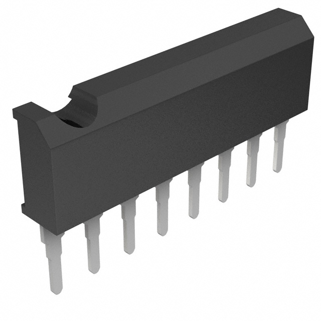
BA10358N
19.3 ± 0.2
2.8 ± 0.2
0.15 ± 0.1
1 3.5 ± 0.5 2.54
8 0.6 0.8 1.3 0.3 ± 0.1
1.15 ± 0.1
1 0.1
4
(0.52)
0.65 0.22 ± 0.1
0.3Min. 0.1
SSOP-B8
SIP8
0.15 ± 0.1
1
4
5
�
很抱歉,暂时无法提供与“BA10358N”相匹配的价格&库存,您可以联系我们找货
免费人工找货