Standard ICs
Dual high slew rate, low noise operational amplifier
BA15532 / BA15532F / BA15532N
The BA15532, BA15532F, and BA15532N are low-noise dual operational amplifiers designed especially for applications involving high-grade audio equipment. Since they feature low noise, a wide band width, and high power output, these products can also be used in measuring instruments and control circuits. The following packages are available : 8-pin DIP (BA15532), 8-pin SOP (BA15532F), and 8-pin SIP (BA15532N).
•Features current capacity. 1) High output
2) High slew rate.
3) Low noise.
•Block diagram
BA15532 / BA15532F BA15532N
OUT1 1 8 VCC
– IN1 2
–
+ IN1 3
1ch
7
OUT2
1ch
+ +
2ch
+ –
+ 2ch –
–
6
– IN2
1
2
3
4
5
6
7 OUT2
VEE 4
5
+ IN2 OUT1 – IN1 + IN1 + IN2 – IN2 VCC VEE
8
1
�Standard ICs
BA15532 / BA15532F / BA15532N
VCC
•Internal circuit configuration
+ IN
– IN
OUT
VEE
•Absolute maximum ratings (Ta = 25°C)
Parameter Power supply voltage Power dissipation Differential input voltage Common-mode input voltage Operating temperature Storage temperature Symbol VCC Pd VID VI Topr Tstg Limits BA15532 ± 21 800∗ ± 0.5 – VCC ~ VCC – 20 ~ + 75 BA15532F ± 21 550∗ ± 0.5 – VCC ~ VCC – 20 ~ + 75 BA15532N ± 21 900∗ ± 0.5 – VCC ~ VCC – 20 ~ + 75 Unit V mW V V °C °C
– 55 ~ + 125 – 55 ~ + 125 – 55 ~ + 125
∗ Refer to Pd characteristics diagram.
The values for the BA15532F are those when it is mounted on a glass epoxy board (50mm × 50mm × 1.6mm).
CC
•Electrical characteristics (unless otherwise noted, Ta = 25°C, V
Parameter Input offset voltage Input offset current Input bias current High-amplitude voltage gain Common-mode input voltage Maximum output voltage Maximum output voltage Common-mode rejection ratio Power supply voltage rejection ratio Quiescent current Output short-circuit current Slew rate Voltage gain band width Maximum frequency Input conversion noise voltage Channel separation Symbol VIO IIO IB AV VICM VOM VOM CMRR PSRR IQ IOS S. R. GBW fT Vn CS Min. — — — 80 ± 12 ± 12 ± 15 70 80 — — — — — — — Typ. 0.5 10 200 94 ± 13 ± 13 ± 16 100 100 8 38 8 20 7 0.7 110
= + 15V, VEE = - 15V)
Unit mV nA nA dB V V V dB dB mA mA V / µs MHz MHz µV dB RIAA, RS = 100Ω, BW = 20Hz ~ 30kHz RIAA, f = 1kHz AV = 1, RL = 600Ω, CL = 100pF CL = 100pF, RL = 600Ω, f = 10kHz RS = 50Ω, RL RL RL RL RL RL RL RL 10kΩ 10kΩ 600Ω, VO = ± 10V 10kΩ 600Ω 600Ω, VCC = 18V, VEE = – 18V 10kΩ 10kΩ Conditions 10kΩ
Max. 4 150 800 — — — — — — 16 — — — — 1.5 —
RS = 50Ω, RL
RL = ∞, on All Op - Amps
2
�Standard ICs
BA15532 / BA15532F / BA15532N
•Electrical characteristic curves
1200 POWER DISSIPATION: Pd (mW) QUIESCENT CURRENT: IQ (mA) 10 OPEN LOOP VOLTAGE GAIN: Av (dB) 0 ± 10 ± 20
±
120
1000 BA15532N 800 BA15532 600
8
100 80
6
60
4
400 BA15532F 200 0
40
2
20 0 10
0 0 25 50 75 100 125 150 AMBIENT TEMPERATURE: Ta (°C)
100
1k
10k
100k
1M
10M
POWER SUPPLY VOLTAGE: VCC (V)
FREQUENCY: f (Hz)
Fig.1 Power dissipation vs. ambient temperature
Fig.2 Quiescent current vs. power supply voltage
Fig.3 Open loop voltage gain vs. frequency
32 MAXIMUM OUTPUT VOLTAGE: VOM (V) 28 24 20 16 12 8 4 0 100 1k 10k
V = ± 15V INPUT BIAS CURRENT: IB (µA) INPUT BIAS CURRENT: IB (µA) V = ± 15V 0.3
±
±
0.4
0.4
0.3
0.2
0.2
0.1
100k
1M
0.1 – 40
– 20
0
20
40
60
80
0
10
20
30
+
40
FREQUENCY: f (Hz)
AMBIENT TEMPERATURE: Ta (°C)
POWER SUPPLY VOLTAGE: V (V)
Fig.4 Maximum output voltage vs. frequency
Fig.5 Input bias current vs. ambient temperature
Fig.6 Input bias current vs. power supply voltage
5 0
–5
INPUT COMMON MORE VOLTAGE RANGE: VICM (V)
± 20
OUTPUT VOLTAGE VOUT (V)
± 10
INPUT VOLTAGE VIN (V)
5 0
–5 0 2 4 TIME (µs) 6 8
0
± 10
± 20
±
± 30
POWER SUPPLY VOLTAGE: V (V)
Fig.7 Output response characteristics
Fig.8 Common mode input voltage vs. power supply voltage
3
�Standard ICs
BA15532 / BA15532F / BA15532N
VCC
•Operation notes circuits (1) Handling unused
If there are any circuits which are not being used, we recommend making connections as shown in Figure 9, with the non-inverted input pin connected to the potential within the in-phase input voltage range (VICM).
–
To potential in VICM
+
VEE
Fig.9 Unused circuit connections
•External dimensions (Units: mm)
BA15532
9.3 ± 0.3 6.5 ± 0.3 8 5
BA15532F
5.0 ± 0.2 8 6.2 ± 0.3 4.4 ± 0.2 5
1 0.51Min.
4 7.62
3.2 ± 0.2 3.4 ± 0.3
0.11
0.3 ± 0.1
1.5 ± 0.1
1
4
2.54
0.5 ± 0.1 0° ~ 15°
1.27
0.4 ± 0.1
0.3Min. 0.15
DIP8
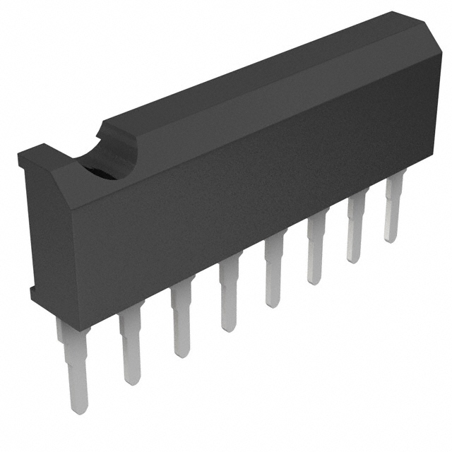
BA15532N
SOP8
19.3 ± 0.2 10.5 ± 0.5 5.8 ± 0.2
2.8 ± 0.2
1.2
1 3.5 ± 0.5 2.54
8 0.6 0.8 1.3 0.3 ± 0.1
SIP8
4
0.15 ± 0.1
�
很抱歉,暂时无法提供与“BA15532N”相匹配的价格&库存,您可以联系我们找货
免费人工找货