Datasheet
Dual Output Fixed Output
LDO Regulators
BA3258HFP BA33Dxx series
●General Description
The BA3258HFP, BA33D15HFP, BA33D18HFP are fixed 2-output low-saturation regulators with a voltage accuracy at both
outputs of ±2%. These series incorporate both overcurrent protection and thermal shutdown (TSD) circuits in order to
prevent damage due to output short-circuiting and overloading, respectively.
●Features
Output voltage accuracy: ±2%.
A ceramic capacitor can be used to prevent output
oscillation (BA3258HFP).
High Ripple Rejection (BA33Dxx Series)
Built-in thermal shutdown circuit
Built-in overcurrent protection circuit
●Key Specifications
Input Power Supply Voltage:
BA3258HFP
BA33Dxx Series
Output voltage range:
Output current: BA3258HFP
BA33Dxx Series
Operating temperature range:
BA3258HFP
BA33Dxx Series
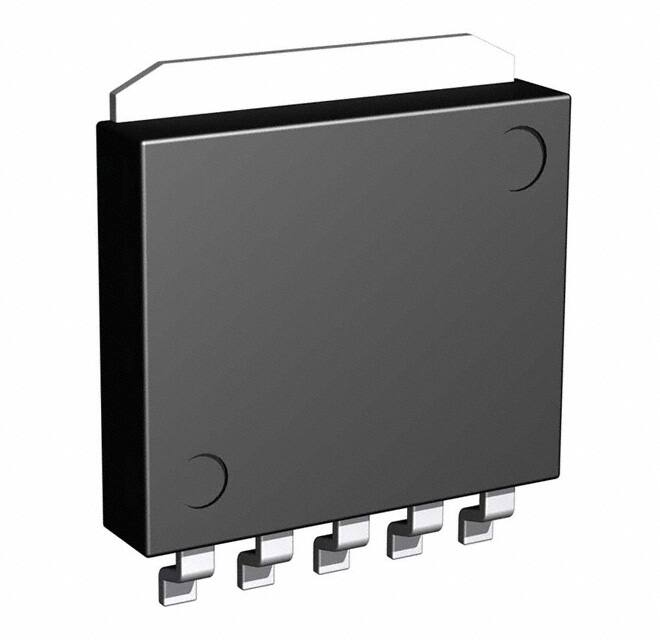
●Package
HRP5
W (Typ.) x D (Typ.) x H (Max.)
9.395mm x 10.54 mm x 2.005mm
14.0V(Max.)
16.0V(Max.)
Fixed
1A (Max.)
0.5A(Max.)
HRP5
-30℃ to 85℃
-25℃ to 105℃
●Applications
FPDs, TVs, PCs, DSPs in DVDs and CDs
●Ordering Information
B
A
3
x
x
x
H
F
P
-
Packaging and forming specification
TR: Embossed tape and reel
(HRP5)
Package
HFP:HRP5
Part
Number
●Lineup
Maximum output current
(Max.)
1A
0.5A
Output Voltage 1
(Typ.)
3.3V
3.3V
3.3V
○Product structure:Silicon monolithic integrated circuit
www.rohm.com
© 2012 ROHM Co., Ltd. All rights reserved.
TSZ22111・14・001
TR
Output Voltage 2
(Typ.)
1.5V
1.5V
1.8V
Package
HRP5
Orderable Part Number
Reel of 2000
BA3258HFP-TR
BA33D15HFP-TR
BA33D18HFP-TR
○This product is not designed protection against radioactive rays.
1/15
TSZ02201-0R6R0A600090-1-2
26.2012 Rev.001
�Datasheet
BA3258HFP BA33Dxx series
●Block Diagrams / Standard Example Application Circuits / Pin Configurations / Pin Descriptions
BA3258HFP
VO1
5
Current
Limit
VO2
4
GND
3
Current
Limit
GND
Thermal
Shutdown
FIN
3.3V
Pin No.
Pin name
CO1
1
VCC
1μF
2
V02_S
Output voltage monitor pin
3
GND
GND pin
4
VO2
1.5V output pin
5
VO1
3.3V output pin
FIN
GND
1.5V
CO2
1μF
Function
Power supply pin
GND pin
TOP VIEW
2
V0 2_S
PIN
VC C
1
VR EF
V IN
CIN
3.3μF
External capacitor
setting range
VCC (1 Pin)
Approximately 3.3µF
VO1 (5 Pin)
1µF to 1000µF
VO2 (4 Pin)
1µF to 1000µF
1
2
3
4
5
HRP5
Fig.1 BA3258HFP Block Diagram
BA33DxxSeries
GND(Fin)
VC C
V CC
Pin No.
Reference
Voltage
Current
Limit
Sat.
Prevention
V CC
VC C
Pin name
Function
1
VCC
Power supply pin
2
N.C.
N.C. pin
3
GND
GND pin
4
VO1
3.3V output pin
5
FIN
VO2
1.5V/1.8V output pin
GND
GND pin
*The N.C. pin is not electrically connected internally
Thermal
Shut Down
VC C
1
N.C.
Current
Limit
2
3
GND
1μF
Sat.
Prevention
V O1
4
CO
10μF
TOP VIEW
VO 2
5
CO
10μF
PIN
External capacitor
setting range
VCC (1 Pin)
Approximately 3.3µF
VO1 (4 Pin)
10µF to 1000µF
VO2 (5 Pin)
10µF to 1000µF
1
2
3
4
5
HRP5
Fig.2 BA33Dxx Series Block Diagram
www.rohm.com
© 2012 ROHM Co., Ltd. All rights reserved.
TSZ22111・15・001
2/15
TSZ02201-0R6R0A600090-1-2
26.2012 Rev.001
�Datasheet
BA3258HFP BA33Dxx series
●Absolute Maximum Ratings
BA3258HFP
Parameter
BA33Dxx Series
Symbol
Ratings
Unit
Applied voltage
VCC
15*1
V
Power dissipation
Pd*2
2300*2
mW
Topr
−30 to 85
℃
Tstg
−55 to 150
℃
Tjmax
150
℃
Operating
temperature range
Ambient storage
temperature
Maximum junction
temperature
Parameter
Symbol
Ratings
Unit
Applied voltage
VCC
18*1
V
Power dissipation
Pd*2
2300*2
mW
Topr
−25 to 105
℃
Tstg
−55 to 150
℃
Tjmax
150
℃
Operating
temperature range
Ambient storage
temperature
Maximum junction
temperature
*1 Must not exceed Pd
*2. Derated at 18.4 mW/℃ at Ta>25℃ when mounted on a glass epoxy board (70 mm × 70 mm × 1.6 mm)
●Recommended Operating Ratings
BA3258HFP
Parameter
BA33DxxSeries
Ratings
Symbol
Min. Typ. Max.
Unit
Parameter
Symbol
Min.
Ratings
Typ. Max.
Unit
Input power supply
voltage
VCC
4.75
-
14.0
V
Input power supply
voltage
VCC
4.1
-
16.0
V
3.3 V output current
IO1
-
-
1
A
3.3 V output current
IO1
-
-
0.5
A
1.5 V output current
IO2
-
-
1
A
1.5V output current
IO2
-
-
0.5
A
1.8 V output current
IO2
-
-
0.5
A
●Electrical Characteristics
BA3258HFP (Unless otherwise specified, Ta = 25℃, VCC = 5 V)
Limits
Parameter
Symbol
Min.
Typ.
Bias current
IB
-
3
Max.
5
Unit
mA
Conditions
IO1=0mA,IO2=0mA
[3.3 V Output Block]
Output voltage1
VO1
Minimum output voltage difference 1
∆VD1
-
1.1
IO1
1.0
-
R.R.1
46
52
Output current capacity 1
Ripple rejection 1
3.234 3.300 3.366
V
IO1=50mA
1.3
V
IO1=1A,VCC=3.8V
-
A
-
dB
f=120Hz,ein=0.5Vp-p,IO1=5mA
Input stability 1
Reg.I1
-
5
15
mV
VCC=4.75→14V,IO1=5mA
Load stability 1
Temperature coefficient of output
voltage 1*3
[1.5 V Output Block]
Reg.L1
-
5
20
mV
IO1=5mA→1A
TCVO1
-
±0.01
-
Output voltage 2
VO2
Output current capacity 2
IO2
1.0
-
-
A
R.R.2
46
52
-
dB
Ripple rejection 2
1.470 1.500 1.530
%/℃ IO1=5mA,Tj=0℃ to 85℃
V
IO2=50mA
f=120Hz,ein=0.5Vp-p,IO2=5mA
Input stability 2
Reg.I2
-
5
15
mV
VCC=4.1→14V,IO2=5mA
Load stability 2
Temperature coefficient of output
voltage 2*3
Reg.L2
-
5
20
mV
IO2=5mA→1A
TCVO2
-
±0.01
-
%/℃ IO2=5mA,Tj=0℃ to 125℃
*3: Not 100% tested.
www.rohm.com
© 2012 ROHM Co., Ltd. All rights reserved.
TSZ22111・15・001
3/15
TSZ02201-0R6R0A600090-1-2
26.2012 Rev.001
�Datasheet
BA3258HFP BA33Dxx series
●Electrical Characteristics - continued
BA33Dxx Series (Unless otherwise specified, Ta = 25℃, VCC = 5 V)
Limits
Parameter
Symbol
Min.
Typ.
Bias current
IB
-
0.7
Max.
1.6
Unit
mA
Conditions
IO1=0mA,IO2=0mA
[3.3V Output Block]
Output voltage 1
VO1
V
IO1=250mA
Minimum output voltage difference 1
∆VD1
-
0.25
0.50
V
IO1=250mA,VCC=3.135V
IO1
0.5
-
-
A
Ripple rejection 1
R.R.1
50
58
-
dB
f=120Hz,ein=1Vp-p,IO1=200mA
Input stability 1
Reg.I1
-
5
30
mV
VCC=4.1V→16V,IO1=250mA
Load stability 1
Temperature coefficient of output
voltage 1*3
Reg.L1
-
30
75
mV
IO1=0mA→0.5A
TCVO1
-
±0.01
-
Output current capacity 1
3.234 3.300 3.366
%/℃ IO1=5mA,Tj=0℃ to 125℃
BA33D15HFP VO2 output
[1.5V Output Block]
Output voltage 2
Output current capacity 2
VO2
1.470 1.500 1.530
V
IO2=250mA
IO2
0.5
-
-
A
Ripple rejection 2
R.R.2
50
58
-
dB
f=120Hz,ein=1Vp-p,IO2=200mA
Input stability 2
Reg.I2
-
5
30
mV
VCC=4.1V→16V,IO2=250mA
Load stability 2
Temperature coefficient of output
voltage 2*3
Reg.L2
-
30
75
mV
IO2=0mA→0.5A
TCVO2
-
±0.01
-
%/℃ IO2=5mA,Tj=0℃ to 125℃
BA33D18HFP VO2 output
[1.8V Output Block]
Output voltage 2
Output current capacity 2
VO2
1.764 1.800 1.836
V
IO2=250mA
IO2
0.5
-
-
A
Ripple rejection 2
R.R.2
50
58
-
dB
f=120Hz,ein=1Vp-p,IO2=200mA
Input stability 2
Reg.I2
-
5
30
mV
VCC=4.1V→16V,IO2=250mA
Load stability 2
Temperature coefficient of output
*3
voltage 2
Reg.L2
-
30
75
mV
IO2=0mA→0.5A
TCVO2
-
±0.01
-
%/℃ IO2=5mA,Tj=0℃ to 125℃
*3: Not 100% tested.
www.rohm.com
© 2012 ROHM Co., Ltd. All rights reserved.
TSZ22111・15・001
4/15
TSZ02201-0R6R0A600090-1-2
26.2012 Rev.001
�Datasheet
BA3258HFP BA33Dxx series
ICC
●Typical Performance Curves
BA3258HFP (Unless otherwise specified, Ta = 25℃, VCC = 5V)
Fig.3
Circuit Current
(with no load)
ICC
Fig.4
Circuit Current vs. Load Current IO1
(IO1 = 0 →1 A)
Fig.6
Input Stability
(3.3 V output with no load)
Fig.5
Circuit Current vs. Load Current IO2
(IO2 = 0 → 1 A)
www.rohm.com
© 2012 ROHM Co., Ltd. All rights reserved.
TSZ22111・15・001
5/15
TSZ02201-0R6R0A600090-1-2
26.2012 Rev.001
�Datasheet
BA3258HFP BA33Dxx series
●Typical Performance Curves - continued
Fig.8
Load Stability
(3.3 V output)
Fig.7
Input Stability
(1.5 V output with no load)
Fig.10
I/O Voltage Difference (3.3 V output)
(VCC = 3.8 V, IO1 = 0 → 1 A)
Fig.9
Load Stability
www.rohm.com
© 2012 ROHM Co., Ltd. All rights reserved.
TSZ22111・15・001
6/15
TSZ02201-0R6R0A600090-1-2
26.2012 Rev.001
�Datasheet
BA3258HFP BA33Dxx series
●Typical Performance Curves - continued
R.R.(1.5 V output)
R.R.(3.3 V output)
Fig.11
R.R. Characteristics
(ein = 0.5 VP-P, IO = 5 mA)
IB
Fig.12
Output Voltage vs Temperature
(3.3 V output)
Fig.13
Output Voltage vs Temperature
(1.5 V output)
www.rohm.com
© 2012 ROHM Co., Ltd. All rights reserved.
TSZ22111・15・001
Fig.14
Circuit Current vs Temperature
(IO = 0 mA)
7/15
TSZ02201-0R6R0A600090-1-2
26.2012 Rev.001
�Datasheet
BA3258HFP BA33Dxx series
●Typical Performance Curves - continued
BA33D15HFP (Unless otherwise specified, Ta = 25℃, VCC = 5V)
Fig.15
Circuit Current
(with no load)
Fig.16
Circuit Current vs Load Current IO1
(IO1 = 0 → 500 mA)
Fig.17
Circuit Current vs Load Current IO2
(IO2 = 0 → 500 mA)
www.rohm.com
© 2012 ROHM Co., Ltd. All rights reserved.
TSZ22111・15・001
Fig.18
Input Stability
(3.3 V output, IO1 = 250 mA)
8/15
TSZ02201-0R6R0A600090-1-2
26.2012 Rev.001
�Datasheet
BA3258HFP BA33Dxx series
●Typical Performance Curves - continued
Fig.19
Input Stability
(1.5 V output, IO2 = 250 mA)
Fig.20
Load Stability
(3.3 V output)
Fig.21
Load Stability
(1.5 V output)
Fig.22
I/O Voltage Difference
(VCC = 3.135 V, 3.3 V output)
www.rohm.com
© 2012 ROHM Co., Ltd. All rights reserved.
TSZ22111・15・001
9/15
TSZ02201-0R6R0A600090-1-2
26.2012 Rev.001
�Datasheet
BA3258HFP BA33Dxx series
●Typical Performance Curves - continued
Vo2(1.5V output)
Vo1(3.3V output)
Fig.23
R.R. Characteristics
(ein = 1 VP-P, IO = 100 mA)
IB[uA]
Fig.24
Output Voltage vs. Temperature
(3.3 V output)
Fig.26
Circuit Current vs Temperature
(IO = 0 mA)
Fig.25
Output Voltage vs. Temperature
(1.5 V output)
www.rohm.com
© 2012 ROHM Co., Ltd. All rights reserved.
TSZ22111・15・001
10/15
TSZ02201-0R6R0A600090-1-2
26.2012 Rev.001
�Datasheet
BA3258HFP BA33Dxx series
●I/O equivalence circuit
BA3258HFP
BA33DxxSeries
VCC
VCC
VCC
VO1/VO2
VO2
VO1
V02_S
Fig.27 BA3258HFP I/O equivalence circuit
Fig.28 BA33Dxx Series I/O equivalence circuit
●Power Dissipation
If the IC is used under excessive power dissipation conditions, the chip temperature will rise, which will have an adverse
effect on the electrical characteristics of the IC, such as a reduction in current capability. Furthermore, if the temperature
exceeds Tjmax, element deterioration or damage may occur. Implement proper thermal designs to ensure that the power
dissipation is within the permissible range in order to prevent instantaneous IC damage resulting from heat and maintain the
reliability of the IC for long-term operation. Refer to the power derating characteristics curves in Fig.29.
・Power Consumption (Pc) Calculation Method
VCC
VCC
IP
3.3 V output
IO1
*VCC: Applied voltage
IO1:Load current on VO1 side
IO2:Load current on VO2 side
ICC:Circuit current
* The ICC (circuit current) varies with the load.
(See reference data in Fig.4, 5, 16, and 17.)
・Power consumption of 3.3V power transistor:
V
Controller
PC1 = (VCC − 3.3) × IO1
V
I
・Power consumption of VO2 power transistor:
Power Tr
V
PC2 = (VCC − VO2) × IO2
I
1.5 V output or
・Power consumption due to circuit current:
GND
1.8 V output
PC3 = VCC × ICC
→PC = PC1 + PC2 + PC3
Refer to the above and implement proper thermal designs so that the IC will not be used under excessive power dissipation
conditions under the entire operating temperature range.
O1
CC
O2
O2
CC
・Calculation example (BA33D15HFP)
Example: VCC = 5V, IO1 = 200mA, and IO2 = 100mA
・Power consumption of 3.3V power transistor:
・Power consumption of 1.5V power transistor:
・Power consumption due to circuit current:
PC1 = (VCC − 3.3) × IO1 = (5 − 3.3) × 0.2 = 0.34W
PC2 = (VCC − 1.5) × IO2 = (5 − 1.5) × 0.2 = 0.35W
PC3 = VCC × ICC = 5 × 0.0085 = 0.0425 (W) (See Fig.16 and 17)
Implement proper thermal designs taking into consideration the dissipation at full power consumption
(i.e., PC1 + PC2 + PC3 = 0.34 + 0.35 + 0.0425 = 0.7325W).
www.rohm.com
© 2012 ROHM Co., Ltd. All rights reserved.
TSZ22111・15・001
11/15
TSZ02201-0R6R0A600090-1-2
26.2012 Rev.001
�Datasheet
BA3258HFP BA33Dxx series
●Explanation of External Components
○BA3258HFP
1) Pin 1 (VCC pin)
Connecting a ceramic capacitor with a capacitance of approximately 3.3μF between VCC and GND as close to the pins
as possible is recommended.
2) Pins 4 and 5 (VO pins)
Insert a capacitor between the Vo and GND pins in order to prevent output oscillation. The capacitor may oscillate if
the capacitance changes as a result of temperature fluctuations. Therefore, it is recommended that a ceramic
capacitor with a temperature coefficient of X5R or above and a maximum capacitance change (resulting from
temperature fluctuations) of ±10% be used. The capacitance should be between 1μF and 1,000µF. (Refer to Fig.30)
Board size: 70 mm × 70 × 1.6 mm (with a thermal via incorporated by the board)
9
8 (3) 7.3 W
7
6 (2) 5.5 W
5
4
3 (1) 2.3 W
2
1
0
0
25
Board surface area: 10.5 mm × 10.5 mm
(1)
2-layer board (Backside copper foil area: 15 mm × 15mm)
(2)
2-layer board (Backside copper foil area: 70 mm × 70 mm)
10.0
5.0
(3) 4-layer board (Backside copper foil area: 70 mm × 70mm)
50
75
100
125
150
AMBIENT TEMPERATURE:Ta[℃]
Fig.29 Thermal Derating Curves
www.rohm.com
© 2012 ROHM Co., Ltd. All rights reserved.
TSZ22111・15・001
10.0
5.0
4.0
2.0
1.0
不安定領域
Unstable
region
2.0
1.0
0.5
0.2
0.1
0.05
0.5
0.2
0.15
0.1
0.05
0.02
0.01
0.02
0.01
Stable
region
安定領域
0
200
400 600
Io [mA]
800
1000
Fig.30 BA3258HFP ESR characteristics
12/15
Unstable
region
不安定領域
ESR [Ω]
10
ESR [Ω]
POWER DISSIPATION:Pd [W]
○BA33DxxSeries
1) Pin 1 (VCC pin)
Insert a 1μF capacitor between VCC and GND. The capacitance will vary depending on the application. Check the
capacitance with the application set and implement designing with a sufficient margin.
2) Pins 4 and 5 (VO pins)
Insert a capacitor between the VO and GND pins in order to prevent oscillation. The capacitance may vary greatly with
temperature changes, thus making it impossible to completely prevent oscillation. Therefore, use a tantalum aluminum
electrolytic capacitor with a low ESR (Equivalent Serial Resistance). The output will oscillate if the ESR is too high or
too low, so refer to the ESR characteristics in Fig.31 and operate the IC within the stable operating region. If there is a
sudden load change, use a capacitor with higher capacitance. A capacitance between 10μF and 1,000μF is
recommended.
Stable
region
安定領域
Unstable
region
不安定領域
0
200
400 600
Io [mA]
800
1000
Fig.31 BA33Dxx Series
ESR characteristics
TSZ02201-0R6R0A600090-1-2
26.2012 Rev.001
�Datasheet
BA3258HFP BA33Dxx series
●Operational Notes
1) Absolute maximum ratings
An excess in the absolute maximum ratings, such as supply voltage, temperature range of operating conditions, etc., can break
down the devices, thus making impossible to identify breaking mode, such as a short circuit or an open circuit. If any over rated
values will expect to exceed the absolute maximum ratings, consider adding circuit protection devices, such as fuses.
2) GND voltage
The potential of GND pin must be minimum potential in all operating conditions.
3) Thermal Design
Use a thermal design that allows for a sufficient margin in light of the power dissipation (Pd) in actual operating
conditions.
4) Inter-pin shorts and mounting errors
Use caution when positioning the IC for mounting on printed circuit boards. The IC may be damaged if there is any
connection error or if pins are shorted together.
5) Actions in strong electromagnetic field
Use caution when using the IC in the presence of a strong electromagnetic field as doing so may cause the IC to
malfunction.
6) Testing on application boards
When testing the IC on an application board, connecting a capacitor to a pin with low impedance subjects the IC to stress.
Always discharge capacitors after each process or step. Always turn the IC's power supply off before connecting it to or
removing it from a jig or fixture during the inspection process. Ground the IC during assembly steps as an antistatic
measure. Use similar precaution when transporting or storing the IC.
7) Regarding input pin of the IC
This monolithic IC contains P+ isolation and P substrate layers between adjacent elements in order to keep them isolated.
P-N junctions are formed at the intersection of these P layers with the N layers of other elements, creating a parasitic
diode or transistor. For example, the relation between each potential is as follows:
When GND > Pin A and GND > Pin B, the P-N junction operates as a parasitic diode.
When GND > Pin B, the P-N junction operates as a parasitic transistor.
Parasitic diodes can occur inevitable in the structure of the IC. The operation of parasitic diodes can result in mutual
interference among circuits, operational faults, or physical damage. Accordingly, methods by which parasitic diodes
operate, such as applying a voltage that is lower than the GND (P substrate) voltage to an input pin, should not be used.
8) Ground Wiring Pattern
When using both small signal and large current GND patterns, it is recommended to isolate the two ground patterns,
placing a single ground point at the ground potential of application so that the pattern wiring resistance and voltage
variations caused by large currents do not cause variations in the small signal ground voltage. Be careful not to change
the GND wiring pattern of any external components, either.
9) Thermal Shutdown Circuit (TSD)
This IC incorporates a built-in thermal shutdown circuit for protection against thermal destruction. Should the junction
temperature (Tj) reach the thermal shutdown ON temperature threshold, the TSD will be activated, turning off all output
power elements. The circuit will automatically reset once the chip's temperature Tj drops below the threshold temperature.
Operation of the thermal shutdown circuit presumes that the IC's absolute maximum ratings have been exceeded.
Application designs should never make use of the thermal shutdown circuit.
10) Overcurrent protection circuit
An overcurrent protection circuit is incorporated in order to prevention destruction due to short-time overload currents.
Continued use of the protection circuits should be avoided. Please note that the current increases negatively impact the
temperature.
11) Damage to the internal circuit or element may occur when the polarity of the VCC pin is opposite to that of the other pins in
applications. (I.e. VCC is shorted with the GND pin while an external capacitor is charged.) Use a maximum capacitance
of 1000 mF for the output pins. Inserting a diode to prevent back-current flow in series with VCC or bypass diodes
between VCC and each pin is recommended.
Resistor
抵抗
Transistor
(NPN)
トランジスタ(NPN)
B
(端子
(
Pin AA)
)
(端子
(Pin B)
B)
C
~
~
Diode for preventing back current flow
(Pin B)
~
~
Bypass diode
C
E
~
~
B
V
CC
VCC
GND
GND
N
P
P+
P+
N
P+
Parasitic elements or
N
N
transistors
(Pin A)
P substrate
寄生素子
Parasitic
elements
GND
Fig.32 Bypass diode
N
N
N
N
N
P substrate
P 基板
P
P
P+
~
~
Output pin
E
P 基板
Parasitic elements
Parasitic elements
GND
GND
Fig.33 Example of Simple Bipolar IC Architecture
Status of this document
The Japanese version of this document is formal specification. A customer may use this translation version only for a reference
to help reading the formal version.
If there are any differences in translation version of this document formal version takes priority.
www.rohm.com
© 2012 ROHM Co., Ltd. All rights reserved.
TSZ22111・15・001
13/15
TSZ02201-0R6R0A600090-1-2
26.2012 Rev.001
�Datasheet
BA3258HFP BA33Dxx series
●Physical Dimension Tape and Reel Information
HRP5
8.82 ± 0.1
(6.5)
0.08±0.05
1.2575
1
2
3
4
0.835±0.2
1.523±0.15
8.0±0.13
(7.49)
1.905±0.1
Tape
Embossed carrier tape
Quantity
2000pcs
Direction
of feed
10.54±0.13
1.017±0.2
9.395±0.125
(MAX 9.745 include BURR)
TR
direction is the 1pin of product is at the upper right when you hold
( The
)
reel on the left hand and you pull out the tape on the right hand
1pin
5
+5.5°
4.5°−4.5°
+0.1
0.27 −0.05
1.72
0.73±0.1
0.08 S
S
Direction of feed
Reel
(Unit : mm)
∗ Order quantity needs to be multiple of the minimum quantity.
●Marking Diagram
HRP5 (TOP VIEW)
Part Number Marking
LOT Number
1PIN MARK
Part Number
Package
Part Number Marking
BA3258HFP
HRP5
BA3258
BA33D15HFP
HRP5
BA33D15
BA33D18HFP
HRP5
BA33D18
www.rohm.com
© 2012 ROHM Co., Ltd. All rights reserved.
TSZ22111・15・001
14/15
TSZ02201-0R6R0A600090-1-2
26.2012 Rev.001
�Datasheet
BA3258HFP BA33Dxx series
●Revision History
Date
Revision
26.Jun.2012
001
Changes
New Release
www.rohm.com
© 2012 ROHM Co., Ltd. All rights reserved.
TSZ22111・15・001
15/15
TSZ02201-0R6R0A600090-1-2
26.2012 Rev.001
�Datasheet
Notice
●General Precaution
1) Before you use our Products, you are requested to carefully read this document and fully understand its contents.
ROHM shall not be in any way responsible or liable for failure, malfunction or accident arising from the use of any
ROHM’s Products against warning, caution or note contained in this document.
2) All information contained in this document is current as of the issuing date and subject to change without any prior
notice. Before purchasing or using ROHM’s Products, please confirm the latest information with a ROHM sales
representative.
●Precaution on using ROHM Products
1) Our Products are designed and manufactured for application in ordinary electronic equipments (such as AV equipment,
OA equipment, telecommunication equipment, home electronic appliances, amusement equipment, etc.). If you
intend to use our Products in devices requiring extremely high reliability (such as medical equipment, transport
equipment, traffic equipment, aircraft/spacecraft, nuclear power controllers, fuel controllers, car equipment including car
accessories, safety devices, etc.) and whose malfunction or failure may cause loss of human life, bodily injury or
serious damage to property (“Specific Applications”), please consult with the ROHM sales representative in advance.
Unless otherwise agreed in writing by ROHM in advance, ROHM shall not be in any way responsible or liable for any
damages, expenses or losses incurred by you or third parties arising from the use of any ROHM’s Products for Specific
Applications.
2)
ROHM designs and manufactures its Products subject to strict quality control system. However, semiconductor
products can fail or malfunction at a certain rate. Please be sure to implement, at your own responsibilities, adequate
safety measures including but not limited to fail-safe design against the physical injury, damage to any property, which
a failure or malfunction of our Products may cause. The following are examples of safety measures:
[a] Installation of protection circuits or other protective devices to improve system safety
[b] Installation of redundant circuits to reduce the impact of single or multiple circuit failure
3)
Our Products are designed and manufactured for use under standard conditions and not under any special or
extraordinary environments or conditions, as exemplified below. Accordingly, ROHM shall not be in any way
responsible or liable for any damages, expenses or losses arising from the use of any ROHM’s Products under any
special or extraordinary environments or conditions. If you intend to use our Products under any special or
extraordinary environments or conditions (as exemplified below), your independent verification and confirmation of
product performance, reliability, etc, prior to use, must be necessary:
[a] Use of our Products in any types of liquid, including water, oils, chemicals, and organic solvents
[b] Use of our Products outdoors or in places where the Products are exposed to direct sunlight or dust
[c] Use of our Products in places where the Products are exposed to sea wind or corrosive gases, including Cl2,
H2S, NH3, SO2, and NO2
[d] Use of our Products in places where the Products are exposed to static electricity or electromagnetic waves
[e] Use of our Products in proximity to heat-producing components, plastic cords, or other flammable items
[f] Sealing or coating our Products with resin or other coating materials
[g] Use of our Products without cleaning residue of flux (even if you use no-clean type fluxes, cleaning residue of
flux is recommended); or Washing our Products by using water or water-soluble cleaning agents for cleaning
residue after soldering
[h] Use of the Products in places subject to dew condensation
4)
The Products are not subject to radiation-proof design.
5)
Please verify and confirm characteristics of the final or mounted products in using the Products.
6)
In particular, if a transient load (a large amount of load applied in a short period of time, such as pulse) is applied,
confirmation of performance characteristics after on-board mounting is strongly recommended. Avoid applying power
exceeding normal rated power; exceeding the power rating under steady-state loading condition may negatively affect
product performance and reliability.
7)
De-rate Power Dissipation (Pd) depending on Ambient temperature (Ta). When used in sealed area, confirm the actual
ambient temperature.
8)
Confirm that operation temperature is within the specified range described in the product specification.
9)
ROHM shall not be in any way responsible or liable for failure induced under deviant condition from what is defined in
this document.
Notice - Rev.003
© 2012 ROHM Co., Ltd. All rights reserved.
�Datasheet
●Precaution for Mounting / Circuit board design
1) When a highly active halogenous (chlorine, bromine, etc.) flux is used, the residue of flux may negatively affect product
performance and reliability.
2)
In principle, the reflow soldering method must be used; if flow soldering method is preferred, please consult with the
ROHM representative in advance.
For details, please refer to ROHM Mounting specification
●Precautions Regarding Application Examples and External Circuits
1) If change is made to the constant of an external circuit, please allow a sufficient margin considering variations of the
characteristics of the Products and external components, including transient characteristics, as well as static
characteristics.
2)
You agree that application notes, reference designs, and associated data and information contained in this document
are presented only as guidance for Products use. Therefore, in case you use such information, you are solely
responsible for it and you must exercise your own independent verification and judgment in the use of such information
contained in this document. ROHM shall not be in any way responsible or liable for any damages, expenses or losses
incurred by you or third parties arising from the use of such information.
●Precaution for Electrostatic
This Product is electrostatic sensitive product, which may be damaged due to electrostatic discharge. Please take proper
caution in your manufacturing process and storage so that voltage exceeding the Products maximum rating will not be
applied to Products. Please take special care under dry condition (e.g. Grounding of human body / equipment / solder iron,
isolation from charged objects, setting of Ionizer, friction prevention and temperature / humidity control).
●Precaution for Storage / Transportation
1) Product performance and soldered connections may deteriorate if the Products are stored in the places where:
[a] the Products are exposed to sea winds or corrosive gases, including Cl2, H2S, NH3, SO2, and NO2
[b] the temperature or humidity exceeds those recommended by ROHM
[c] the Products are exposed to direct sunshine or condensation
[d] the Products are exposed to high Electrostatic
2)
Even under ROHM recommended storage condition, solderability of products out of recommended storage time period
may be degraded. It is strongly recommended to confirm solderability before using Products of which storage time is
exceeding the recommended storage time period.
3)
Store / transport cartons in the correct direction, which is indicated on a carton with a symbol. Otherwise bent leads
may occur due to excessive stress applied when dropping of a carton.
4)
Use Products within the specified time after opening a humidity barrier bag. Baking is required before using Products of
which storage time is exceeding the recommended storage time period.
●Precaution for Product Label
QR code printed on ROHM Products label is for ROHM’s internal use only.
●Precaution for Disposition
When disposing Products please dispose them properly using an authorized industry waste company.
●Precaution for Foreign Exchange and Foreign Trade act
Since our Products might fall under controlled goods prescribed by the applicable foreign exchange and foreign trade act,
please consult with ROHM representative in case of export.
●Precaution Regarding Intellectual Property Rights
1) All information and data including but not limited to application example contained in this document is for reference
only. ROHM does not warrant that foregoing information or data will not infringe any intellectual property rights or any
other rights of any third party regarding such information or data. ROHM shall not be in any way responsible or liable
for infringement of any intellectual property rights or other damages arising from use of such information or data.:
2)
No license, expressly or implied, is granted hereby under any intellectual property rights or other rights of ROHM or any
third parties with respect to the information contained in this document.
Notice - Rev.003
© 2012 ROHM Co., Ltd. All rights reserved.
�Datasheet
●Other Precaution
1) The information contained in this document is provided on an “as is” basis and ROHM does not warrant that all
information contained in this document is accurate and/or error-free. ROHM shall not be in any way responsible or
liable for any damages, expenses or losses incurred by you or third parties resulting from inaccuracy or errors of or
concerning such information.
2)
This document may not be reprinted or reproduced, in whole or in part, without prior written consent of ROHM.
3)
The Products may not be disassembled, converted, modified, reproduced or otherwise changed without prior written
consent of ROHM.
4)
In no event shall you use in any way whatsoever the Products and the related technical information contained in the
Products or this document for any military purposes, including but not limited to, the development of mass-destruction
weapons.
5)
The proper names of companies or products described in this document are trademarks or registered trademarks of
ROHM, its affiliated companies or third parties.
Notice - Rev.003
© 2012 ROHM Co., Ltd. All rights reserved.
�


 工商网监
湘ICP备2023018690号
工商网监
湘ICP备2023018690号
