Secondary LDO Regulators
Secondary Fixed Output LDO Regulators
BA□□JC5 Series
Secondary Variable Output LDO Regulator
BA00JC5WT
No.11024EBT03
Description The BA□□JC5 are low-saturation regulators with an output current of 1.5 A and a voltage accuracy of 1%. A broad output voltage range is offered, from 1.5V to 12V, and built-in overcurrent protection and thermal shutdown (TSD) circuits prevent damage due to short-circuiting and overloading, respectively. Features 1) Output current: 1.5A (min.) 2) Output voltage accuracy: 1% 3) Broad output voltage range available: 1.5V -12V (BA□□JC5 series) 4) Low saturation-voltage type with PNP output 5) Built-in overcurrent protection circuit 6) Built-in thermal shutdown circuit 7) Integrated shutdown switch (BA□□JC5WT) 8) Operating temperature range: −40℃ to +105℃
Applications All electronic devices that use microcontrollers and logic circuits
www.rohm.com © 2011 ROHM Co., Ltd. All rights reserved.
1/10
2011.02 - Rev.B
�BA□□JC5 Series,BA00JC5WT
Product Lineup Part Number BA□□JC5T BA□□JC5WT 1.5 1.8 2.5 3.0 3.3 5.0 6.0 6.3 8.0 9.0 12.0 Variable
Technical Note
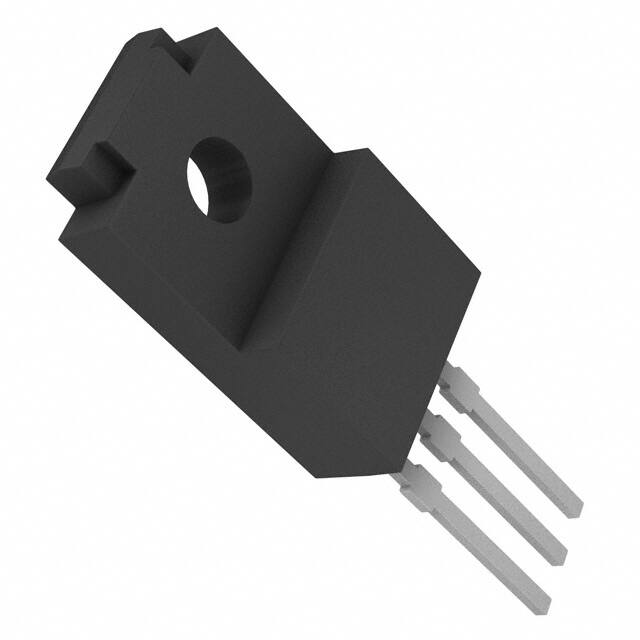
Package TO220FP-3 TO220FP-5 (V5)
Part Number: BA□□JC5□ □ a bc Symbol □□ 15 a 18 25 30 33 50 b c Output voltage (V) 1.5 V typ 1.8 V typ 2.5 V typ 3.0 V typ 3.3 V typ 5.0 V typ Description Output voltage specification □□ 60 63 80 90 J2 00 Output voltage (V) 6.0 V typ 6.3 V typ 8.0 V typ 9.0 V typ 12.0 V typ Variable
Existence of switch With W: A shutdown switch is provided. Without W: No shutdown switch is provided. Package T: TO20FP-5, TO220FP-5V5, TO220FP-3
Absolute Maximum Ratings (Ta = 25℃) Parameter Power supply voltage TO220FP-3 Power dissipation TO220FP-5 TO220FP-5V5 Operating temperature range Ambient storage temperature Maximum junction temperature
*1 *2 Must not exceed Pd Derated at 16mW/℃ at Ta>25℃
Symbol VCC
Ratings 18*1 2000*2
Unit V
Pd
2000*2 2000*2
mW
Topr Tstg Tjmax
−40 to +105 −55 to +150 150
℃ ℃ ℃
Recommended Operating Conditions Parameter Input power supply voltage Input power supply voltage Output current Variable output voltage setting value
*3 *4 When output voltage is 1.5 V, 1.8 V, or 2.5 V. When output voltage is 3.0 V or higher.
Symbol VCC*3 VcC*4 Io Vo
Ratings Min. 3.0 Vo + 1.0 1.5 Max. 16.0 16.0 1.5 12
Unit V V A V
www.rohm.com © 2011 ROHM Co., Ltd. All rights reserved.
2/10
2011.02 - Rev.B
�BA□□JC5 Series,BA00JC5WT
Electrical Characteristics BA□□JC5T(Unless otherwise specified, Ta = 25℃; Vcc = VCCDC*5) Limits Parameter Symbol Min. Typ. Output voltage Minimum I/O voltage difference*6 Output current capacity Input stability*7 Load stability Temperature coefficient of output voltage*8 Vo ∆Vd Io Reg.I Reg.L Tcvo Vo (T) 0.99 1.5 Vo (T) 0.3 5 5 0.02
Technical Note
Max. Vo (T) 1.01 0.5 60 60 -
Unit V V A mV mV %/℃
Conditions Io = 200 mA Io = 200 mA, Vcc = 0.95 Vo
Vcc = Vo + 1.0 V→16 V, Io = 200 mA Io = 5 mA→1.5 A Io = 5 mA, Tj = 0℃ to 125℃
Vo (T): Set output voltage *5 Vo = 1.5 V, 1.8 V, 2.5 V : Vcc = 3.3 V, Vo = 3.0 V, 3.3 V : Vcc = 5 V, Vo = 5.0 V : Vcc : 8 V, Vo = 6.0 V, 6.3 V : Vcc = 9.0 V, Vo = 8.0 V : Vcc = 11 V, Vo = 9.0 V : Vcc = 12 V, Vo = 12 V : Vcc = 15 V *6 Vo ≥ 3.3 V *7 Change Vcc from 3.0 V to 16 V if 1.5 V ≤ Vo ≤ 2.5 V. *8 Operation guaranteed
BA00JC5WT (−V5)(Unless otherwise specified, Ta = 25℃, Vcc = 3.3 V, VCTL = 3 V, R1 = 30 k, R2 = 30 k*9) Limits Parameter Symbol Unit Conditions Min. Typ. Max. Reference voltage Shutdown circuit current Minimum I/O voltage difference Output current capacity Input stability Load stability Temperature coefficient of output voltage*10
*9 *10
Vo Isd ∆Vd Io Reg.I Reg.L Tcvo
1.2375 1.5 -
1.250 0 0.3 5 5 0.02
1.2625 10 0.5 60 60 -
V A V A mV mV %/℃
Io = 50 mA VCTL = 0 V while in OFF mode Io = 500 mA, Vcc = 2.5 V
Vcc = 4.5 V→16 V, Io = 200 mA Io = 5 mA →1.5 A Io = 5 mA, Tj = 0℃ to 125℃
VOUT = Vc (R1 + R2) / R1 (V) Design guarantee (No total shipment inspection is made.)
www.rohm.com © 2011 ROHM Co., Ltd. All rights reserved.
3/10
2011.02 - Rev.B
�BA□□JC5 Series,BA00JC5WT
Technical Note
Electrical Characteristics Curves (Unless otherwise specified, Ta = 25℃; Vcc = 8 V; VCTL = 3 V; IO = 0 mA)
0.6 CI RCUI T CURRENT : Icc [mA] 0.5
6
6
[BA50JC5T] [BA50JC5T]
0.4 0.3 0.2 0.1 0 0 2 4 6 8 10 12 14 SUPPLY VOLTAGE : V cc [V] 16
[BA50JC5T]
OUTPUT VOLTAGE : VOUT [V] 5 4 3 2 1 0
OUTPUT VOLTAGE : VOUT [V]
5 4 3 2 1 0 0 2 4 6 8 10 12 14 SUPPLY VOLTAGE : Vc c [V] 16
0
2
4 6 8 10 12 14 SUPPLY VOLTAGE : Vc c [V]
16
Fig.1 Circuit Current
6
0.6
Fig.2 Input Stability(Io=0mA)
80 RIPPLE REJECTION : R .R. [dB] 70 60 50 40 30 20 10 0
10
.3 Input Stability (Io = 1.5 A)
[BA50JC5T]
DROPOUT VO LTAGE : ΔVd [mV]
[BA50JC5T]
OUTPUT VOLTAGE : VOUT [ V] 5 4 3 2 1 0 0 0.5 1 1.5 2 OUTPUT CURRENT : IOUT [A] 2.5
[BA50JC5T]
0.5
0.4
0.3
0.2
0.1
0
0
500 1000 OUTPUT CURRENT : IOUT [ mA]
15 00
100
1000
10000
100000
1000000
FREQUENCY : f [Hz]
Fig.4 Load Stability
10 9 OUTPUT VOLTAGE : VOUT [ V] 8 7 6 5 4 3 2 1 0 -40 -20 0 20 40 60 80 TEMPERATURE : Ta [℃] 100
Fig.5 I/O Voltage Difference
1 90 CIRCUI T CURRENT : Icc [mA]
Fig.6 Ripple Rejection
[BA50JC5T]
CIRCUI T CURRENT : Icc [mA]
0.9 0.8 0.7 0.6 0.5 0.4 0.3 0.2 0.1 0 -40 -20
[BA50JC5T]
80 70 60 50 40 30 20 10 0
[BA50JC5T]
0 20 40 60 80 TEMPERATURE : Ta [℃]
100
0
500 1 000 OUTPUT CURRENT : IOUT [ A]
150 0
Fig.7 Output Voltage vs Temperature
6 OUTPUT VOLTAGE : VOUT [V] 5 CO NTRO L CURRENT : ICTL [ μA] 0.6
Fig.8 Circuit Current Temperature
Fig.9 Circuit Current Classified by Load
8
[BA50JC5T]
O UTPUT VOLTAG E : VOUT [V]
0.5 0.4 0.3 0.2 0.1 0
7 6 5 4 3 2 1 0 100
[BA50JC5T]
[BA50JC5T]
4 3 2 1 0 0 2 4 6 8 CONTROL VOLTAGE : VCTL [V] 10
0
2
4 6 8 10 12 14 16 CONTROL VOLTAG E : VCTL [V]
18
120 140 160 1 80 TEMPERATURE : Ta [℃ ]
200
Fig.10 CTL Voltage vs Output Voltage
Fig.11 CTL Voltage vs CTL Current
Fig.12 Thermal Shutdown Circuit (Io = 5 mA)
www.rohm.com © 2011 ROHM Co., Ltd. All rights reserved.
4/10
2011.02 - Rev.B
�BA□□JC5 Series,BA00JC5WT
Block Diagrams / Standard Example Application Circuits [BA□□JC5T]
Technical Note
Vref
TOP VW
Driver
Pin No. 1 2 3
Pin name Vcc GND OUT
Function Power supply voltage input GND Voltage output
TSD 1 Vcc 2
OCP 3
Vcc
GND
OUT
123
0.33μF 22μF
PIN Vcc (1 Pin) OUT (3 Pin)
External capacit setting range Approximately 0.33 F 22 F to 1000 F
TO220FP-3
Fig.13
[BA00JC5WT]
Vcc Vref Driver
TOP VIEW
Pin No. 1 2 3 4 5
Pin name CTL Vcc GND OUT C
Function Output voltage on/off control Power supply voltage input GND Voltage output ADJ pin
TSD
OCP
1
CTL
2
Vcc
3
GND
4
OUT R2
5
C
R1
PIN Vcc (2 Pin) OUT (4 Pin)
12345 12345
External capacit setting range Approximately 0.33 F 22 F to 1000 F
Vcc 0.33μF 22μF
TO220FP-5 TO220FP-5 (V5)
Fig.14
Input / Output Equivalent Circuits
Vcc
Vcc
* For the BA00JC5WT, connect R1 and R2 externally between the ADJ and GND pins and between the OUT and ADJ pins.
OUT
CTL
27kΩ
2kΩ 31kΩ
R2 R1
Equation: VOUT = Vc (R1 + R2) / R1 (Vc = 1.25 V (Typ.)) The recommended R1 value is approximately 30 k to 150 k.
Fig.15
www.rohm.com © 2011 ROHM Co., Ltd. All rights reserved.
5/10
2011.02 - Rev.B
�BA□□JC5 Series,BA00JC5WT
Thermal Derating Curve TO220FP-3/TO220FP-5/TO220FP-5 (V5)
25 POWER DISSIPATION:Pd [W] (1)20.0 20 15 10 5 0
( 1) When using an infinite heat sink. j-c = 6.25 (°C/W) (2) During IC without heat sink operation. j-a = 62.5 (°C/W)
Technical Note
(2)2.0 0 25 50 75 100 125 150
AMBIENT TEMPERATURE :Ta [°C]
Fig.17 The characteristics of the IC are greatly influenced by the operating temperature. If the temperature exceeds the maximum junction temperature Tjmax, deterioration or damage may occur. Implement proper thermal designs to ensure that power dissipation is within the permissible range in order to prevent instantaneous damage resulting from heat and maintain the reliability of the IC for long-term operation. The following method is used to calculate the power consumption Pc (W): Pc = (Vcc – Vo) Io + Vcc Icca Power dissipation Pd ≥ Pc The load current Io is calculated: Io ≤ Pd − Vcc Icca Vcc − Vo
Vcc Vo IO Icca
: Input voltage : Output current : Load current : Circuit current
Calculation Example: Vcc = 6.0V and Vo = 5.0V at Ta = 85℃ 1.040 − 6.0 Icca 6.0 − 5.0 Io ≤ 860mA (Icca 30mA) Refer to the above and implement proper thermal designs so that the IC will not be used under excessive power dissipation conditions under the entire operating temperature range. The power consumption Pc of the IC in the event of shorting (i.e. the Vo and GND pins are shorted) can be obtained from the following equation: Pc = Vcc (Icca + Ishort) (Ishort: short current) ja = 62.5°C/W −16.0mW/°C 25°C = 2000mW 85°C = 1040mW
www.rohm.com © 2011 ROHM Co., Ltd. All rights reserved.
6/10
2011.02 - Rev.B
�BA□□JC5 Series,BA00JC5WT
Operation Notes Vcc pin Insert a capacitor (0.33 F approx.) between VCC and GND. The capacitance will vary depending on the application. Use a suitable capacitance and implement designs with sufficient margins.
Technical Note
GND pin Verify that there is no potential difference between the ground of the application board and the IC. If there is a potential difference, the set voltage will not be output accurately, resulting in unstable IC operation. Therefore, lower the impedance by designing the ground pattern as wide and as short as possible. CTL pin The CTL pin turns on at an operating power supply voltage of 2.0 V or higher and turns off at 0.8 V or lower. There is no particular order when turning the power supply and CTL pins on or off.
CTL
27 k
2 k 31 k
Fig.18 Input Equivalent Circuit Vo pin Insert a capacitor between the Vo and GND pins in order to prevent output oscillation. 10.0 Oscillation region 2.0
OUT IC 22 F
ESR []
1.0 0.5 Stable region 0.2
0.1 0.075 0.05 Fig.19 Output Equivalent Circuit
Oscillation region 0 200 400 600 800 1000 Io [mA] Fig. 20 IO vs ESR
The capacitance may vary greatly with temperature changes, thus making it impossible to completely prevent oscillation. Therefore, use a tantalum aluminum electrolytic capacitor with a low ESR (Equivalent Serial Resistance). The output will oscillate if the ESR is too high or too low, so refer to the ESR characteristics in Fig. 20 and operate the IC within the stable region. Use a capacitor within a capacitance between 22F and 1,000F.
www.rohm.com © 2011 ROHM Co., Ltd. All rights reserved.
7/10
2011.02 - Rev.B
�BA□□JC5 Series,BA00JC5WT
Technical Note
Notes for use 1. Absolute maximum ratings An excess in the absolute maximum ratings, such as supply voltage, temperature range of operating conditions, etc., can break down the devices, thus making impossible to identify breaking mode, such as a short circuit or an open circuit. If any over rated values will expect to exceed the absolute maximum ratings, consider adding circuit protection devices, such as fuses. 2. 3. 4. GND voltage The potential of GND pin must be minimum potential in all operating conditions. Thermal design Use a thermal design that allows for a sufficient margin in light of the power dissipation (Pd) in actual operating conditions. Inter-pin shorts and mounting errors Use caution when positioning the IC for mounting on printed circuit boards. The IC may be damaged if there is any connection error or if pins are shorted together. Actions in strong electromagnetic field Use caution when using the IC in the presence of a strong electromagnetic field as doing so may cause the IC to malfunction. Testing on application boards When testing the IC on an application board, connecting a capacitor to a pin with low impedance subjects the IC to stress. Always discharge capacitors after each process or step. Always turn the IC's power supply off before connecting it to or removing it from a jig or fixture during the inspection process. Ground the IC during assembly steps as an antistatic measure. Use similar precaution when transporting or storing the IC. Regarding input pin of the IC This monolithic IC contains P+ isolation and P substrate layers between adjacent elements in order to keep them isolated.P-N junctions are formed at the intersection of these P layers with the N layers of other elements, creating a parasitic diode or transistor. For example, the relation between each potential is as follows: When GND > Pin A and GND > Pin B, the P-N junction operates as a parasitic diode. When GND > Pin B, the P-N junction operates as a parasitic transistor. Parasitic diodes can occur inevitable in the structure of the IC. The operation of parasitic diodes can result in mutual interference among circuits, operational faults, or physical damage. Accordingly, methods by which parasitic diodes operate, such as applying a voltage that is lower than the GND (P substrate) voltage to an input pin, should Ground Wiring Pattern When using both small signal and large current GND patterns, it is recommended to isolate the two ground patterns, placing a single ground point at the ground potential of application so that the pattern wiring resistance and voltage variations caused by large currents do not cause variations in the small signal ground voltage. Be careful not to change the GND wiring pattern of any external components, either. Thermal shutdown circuit The IC incorporates a built-in thermal shutdown circuit (TSD circuit). The thermal shutdown circuit (TSD circuit) is designed only to shut the IC off to prevent thermal runaway. It is not designed to protect the IC or guarantee its operation. Do not continue to use the IC after operating this circuit or use the IC in an environment where the operation of this circuit is assumed.
5. 6.
7.
8.
9.
10. Overcurrent Protection Circuit An overcurrent protection circuit is incorporated in order to prevention destruction due to short-time overload currents. Continued use of the protection circuits should be avoided. Please note that the current increases negatively impact the temperature. 11. Damage to the internal circuit or element may occur when the polarity of the Vcc pin is opposite to that of the other pins in applications. (I.e. Vcc is shorted with the GND pin while an external capacitor is charged.) Use a maximum capacitance of 1000μF for the output pins. Inserting a diode to prevent back-current flow in series with Vcc or bypass diodes between Vcc and each pin is recommended.
Resistor 抵抗
Bypass Diode
Transistor (NPN) ) トランジスタ(NPN
(端子 B) (Pin B) C
(端子 ) (Pin AA)
Back current prevention diode
~ ~
B
(Pin B) C
~ ~
E GND N
~ ~
P+ N N
P substrate P 基板
B E GND
VCC
P+
O utput pin
P N
P+
N N
P P
N
P+ N N
Parasitic elements or transistors
P substrate P 基板
Parasitic element
寄生素子
Parasitic element
GND
Parasitic element
GND
GND
Fig. 21 Bypass Diode
Fig. 22 Example of Simple Bipolar IC Architecture
www.rohm.com © 2011 ROHM Co., Ltd. All rights reserved.
8/10
2011.02 - Rev.B
~ ~
N
(Pin A)
�BA□□JC5 Series,BA00JC5WT
●Ordering part number
Technical Note
B
A
0
0
J
C
5
W
Shutdown switch
W : Include
T
Packaging and forming specification None:Tube Contener
Part number
Output voltage 00:Variable Other:Fixed
Current capacity 1.5A
Package T :TO220FP-3 TO220FP-5 TO220FP-5(V5)
TO220FP-3
+0.3 10.0 −0.1
1.8±0.2
+0.3 4.5 −0.1 φ3.2±0.1 +0.2 2.8 −0.1
Container Quantity Direction of feed Tube 500pcs Direction of products is fixed in a container tube
7.0 +0.3 −0.1
+0.4 17.0 −0.2
12.0±0.2
13.5Min.
5.0±0.2
8.0±0.2
1.3 0.8 2.54±0.5 0.55 +0.1 −0.05 2.6±0.5
2.54±0.5
123
(Unit : mm)
∗ Order quantity needs to be multiple of the minimum quantity.
TO220FP-5
1.8±0.2
+0.3 10.0−0.1 +0.3 7.0 −0.1
+0.3 4.5 −0.1 φ3.2±0.1 +0.2 2.8 −0.1
Container Quantity Direction of feed Tube 500pcs Direction of products is fixed in a container tube
+0.4 17.0 −0.2
12.0±0.2
13.5Min.
8.0±0.2 0.7
1.2 0.8
1.778
0.5±0.1 2.85
12345
(Unit : mm)
∗ Order quantity needs to be multiple of the minimum quantity.
www.rohm.com © 2011 ROHM Co., Ltd. All rights reserved.
9/10
2011.02 - Rev.B
�BA□□JC5 Series,BA00JC5WT
Technical Note
TO220FP-5(V5)
1.8±0.2
+ 0.3 10.0 − 0.1 7.0 + 0.3 − 0.1 φ3.2±0.1
+0.3 4.5 −0.1
+0.2 2.8 −0.1
Container Quantity Direction of feed
Tube 500pcs Direction of products is fixed in a container tube
+0.4 17.0 −0.2
12.0±0.2
31.5Max.
8.0±0.2 0.7
(2.0)
17.5
1.2 0.8 0.5±0.1 1.778 4.25 8.15
12345
23.4
(2.85)
25.8
(Unit : mm)
∗ Order quantity needs to be multiple of the minimum quantity.
www.rohm.com © 2011 ROHM Co., Ltd. All rights reserved.
10/10
2011.02 - Rev.B
�Notice
Notes
No copying or reproduction of this document, in part or in whole, is permitted without the consent of ROHM Co.,Ltd. The content specified herein is subject to change for improvement without notice. The content specified herein is for the purpose of introducing ROHM's products (hereinafter "Products"). If you wish to use any such Product, please be sure to refer to the specifications, which can be obtained from ROHM upon request. Examples of application circuits, circuit constants and any other information contained herein illustrate the standard usage and operations of the Products. The peripheral conditions must be taken into account when designing circuits for mass production. Great care was taken in ensuring the accuracy of the information specified in this document. However, should you incur any damage arising from any inaccuracy or misprint of such information, ROHM shall bear no responsibility for such damage. The technical information specified herein is intended only to show the typical functions of and examples of application circuits for the Products. ROHM does not grant you, explicitly or implicitly, any license to use or exercise intellectual property or other rights held by ROHM and other parties. ROHM shall bear no responsibility whatsoever for any dispute arising from the use of such technical information. The Products specified in this document are intended to be used with general-use electronic equipment or devices (such as audio visual equipment, office-automation equipment, communication devices, electronic appliances and amusement devices). The Products specified in this document are not designed to be radiation tolerant. While ROHM always makes efforts to enhance the quality and reliability of its Products, a Product may fail or malfunction for a variety of reasons. Please be sure to implement in your equipment using the Products safety measures to guard against the possibility of physical injury, fire or any other damage caused in the event of the failure of any Product, such as derating, redundancy, fire control and fail-safe designs. ROHM shall bear no responsibility whatsoever for your use of any Product outside of the prescribed scope or not in accordance with the instruction manual. The Products are not designed or manufactured to be used with any equipment, device or system which requires an extremely high level of reliability the failure or malfunction of which may result in a direct threat to human life or create a risk of human injury (such as a medical instrument, transportation equipment, aerospace machinery, nuclear-reactor controller, fuelcontroller or other safety device). ROHM shall bear no responsibility in any way for use of any of the Products for the above special purposes. If a Product is intended to be used for any such special purpose, please contact a ROHM sales representative before purchasing. If you intend to export or ship overseas any Product or technology specified herein that may be controlled under the Foreign Exchange and the Foreign Trade Law, you will be required to obtain a license or permit under the Law.
Thank you for your accessing to ROHM product informations. More detail product informations and catalogs are available, please contact us.
ROHM Customer Support System
http://www.rohm.com/contact/
www.rohm.com © 2011 ROHM Co., Ltd. All rights reserved.
R1120A
�