TECHNICAL NOTE
Power Management LSI Series for Automotive Body Control
Regulator with Voltage
Detector IC
BD3951F
●Description
BD3951F is a 5V LDO system regulator particularly developed for automotive applications. The output current of the
regulator can be drawn up to 150mA, and it has built-in power-on reset and input voltage sense. This device can withstand
50V surge input voltage as well as wide ambient temperature operations from -40℃ to +125℃. The adjustable reset
delay time and detection input voltage allow to meet with wide range of design requirements.
●Features
1) Micro processor power supply 5.0V, Adjustable Reset, Adjustable Comparator.
2) 5V is Pch DMOS type low drop out voltage regulator. Iomax=150mA.
3) Low ESR capacitor (Ceramic Capacitor) is available for the Output Capacitor.
4) Over Current Protection built in to prevent the destruction of IC.
5) Thermal Shut Down is built in to prevent the heat runaway.
6) VCC absolute Maximum Ratings 36V.
7) Vcc peak input voltage 50V (*1)
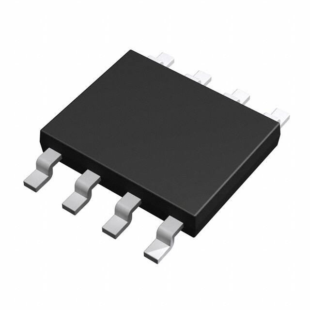
8) Small surface mount package SOP8.
●Applications
·Automotive application (Rain Sensor and Cluster Panel etc.) and all other electronics application.
●Absolute Maximum Ratings (Ta=25℃)
Parameter
Symbol
Limit
Unit
Vcc
-0.3~+36
V
Out Terminal Voltage
Vout
-0.3~+7
V
RES Terminal Voltage
Vres
-0.3~+7
V
SOUT Terminal Voltage
Vsout
-0.3~+7
V
Vcc Input Voltage
RES Output Current
Ires
0.2
mA
SOUT Output Current
Isout
2.5
mA
SIN Input Voltage
Vsin
-0.3~+36 *3
V
Power Dissipation
Pd
687 *2
mV
Topr
-40~+125
℃
Tstg
-55~+150
℃
Vccpeak
50
V
Operating Temperature Range
Storage Temperature Range
Vcc Peak Input Voltage
*1
tr (rising time) is over 1msec, applied voltage is less than 400msec
*2
Pd is derated at 5.5mW/℃ for temperature above Ta=25℃, mounted on 70mm×70mm×1.6mm PCB.
*3
Input current from Vcc to SIN PIN has to be equal and less than 5mA when Vcc voltage is less than SIN PIN voltage.
Dec. 2006
�●Operating Conditions (Ta=-40℃~+125℃)
Symbol
Min.
Typ.
Max.
Unit
Recommended Supply Voltage *4
Parameter
Vcc
6.0
13.5
20
V
Operatinal Supply Voltage *5
Vcc
5.5
13.5
36
V
Reset Adjustable Range
Vdet
4
-
4.7
V
Reset Delay Time Controllable Range
Cct
-
-
10
µF
Vcc Detection Adjustable Range
Vcc
5
-
-
V
*4
The range within test condition of the electrical characteristics.
*5
The range exceeding the test condition of the electrical characteristics.
●Electrical Characteristics(Unless otherwise specified Ta=-40℃~+125℃,Vcc=13.5V)
Parameter
Symbol
Limit
Unit
Condition
Min.
Typ.
Max.
Icc
-
135
210
µA
Iout=0.3mA
Vout
4.90
5.00
5.10
V
Vcc=6~20V,Iout=1~100mA
[Whole Device]
Input Current
[Regulator Block]
Output Voltage
Line Regulation
Lin.Reg
-
10
20
mV
Vcc=6~20V
Load Regulation
Load.Reg
-
15
30
mV
Iout=1~100mA
Dropout Voltage
∆Vd
-
0.31
0.50
V
Iomax
150
-
-
mA
Threshold Voltage
Vdet
Vout
×0.92
Vout
×0.94
Vout
×0.96
V
Hysteresis Voltage
Vhys
50
100
150
mV
Reset Delay Time L->H
TdLH
17
30
-
mS
CT=0.1µF *6
Reset Delay Time H->H
TdHL
-
4
-
µS
CT=0.1µF
RES Pull Up Resistor
Rrst
10
20
40
kΩ
RES Low Output Voltage
VrL
-
0.08
0.40
V
Reset Adjustable Voltage
Vradj
1.18
1.26
1.34
V
Threshold Voltage
Vsdet
1.19
1.26
1.33
V
Hysteresis Voltage
Vsdet off
1.240
1.335
1.430
V
SOUT Pull Up Resistor
Rso
10
20
40
kΩ
SOUT Low Output Voltage
VsL
-
0.06
0.40
V
Vout>4V, Vsin
很抱歉,暂时无法提供与“BD3951F-E2”相匹配的价格&库存,您可以联系我们找货
免费人工找货- 国内价格 香港价格
- 1+26.635551+3.30483
- 10+17.6558610+2.19067
- 25+15.3210225+1.90097
- 100+12.70258100+1.57609


 工商网监
湘ICP备2023018690号
工商网监
湘ICP备2023018690号
