Datasheet
LIN Transceiver for Automotive
BD41030FJ-C BD41030HFN-C
General Description
Key Specifications
◼
◼
◼
BD41030FJ-C,BD41030HFN-C is the best transceiver
for BUS system which need LIN (Local Interconnect
Network) master and slave protocol.
BD41030FJ-C,BD41030HFN-C is low standby electricity
consumption in sleep mode.
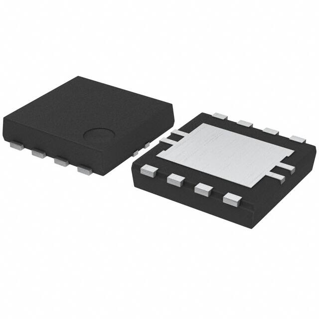
BD41030FJ-C:SOP-J8
BD41030HFN-C:HSON8
◼
◼
Supply Voltage:
Supply Current (Sleep mode):
Supply Current:
(Standby mode; Recessive)
Supply Current:
(Normal mode; Recessive)
Supply Current:
(Normal mode; Dominant)
5V to 27V
1μA to 8μA
100μA to 1000μA
100μA to 1000μA
200μA to 2000μA
Features
◼
◼
◼
◼
◼
◼
◼
◼
Package(s)
Compliant with LIN2.0,LIN2.1,LIN2.2,LIN2.2A
AEC-Q100 Qualified(Note 1)
Absolute maximum ratings of LIN pin is -27V to+40V
Max transmission rate 20kbps
Low Electro Magnetic Emission (EME)
High Electro Magnetic Immunity (EMI)
High impedance at power off for bus
Interface (RXD/TXD) with protocol layer
corresponds to 3.3V/5.0V logic.
◼ Built-in terminator for LIN slave
◼ Standby power consumption in sleep mode
◼ Transmit data(TXD) dominant time-out function
◼ Resistant to LIN-BAT/GND short-circuit
◼ Built-in Thermal Shut Down(TSD)
(Note1:Grade1)
W(Typ) x D(Typ) x H(Max)
4.90mm x 6.00mm x 1.65mm
■SOP-J8
SOP-J8(BD41030FJ-C)
■HSON8
2.90mm x 3.00mm x 0.60mm
Applications
◼ LIN communication for Automotive networks.
HSON8(BD41030HFN-C)
Typical Application Circuit(s)
VECU
LIN
Bus line
5V/3.3V
VIN
Regulator
100nF
100nF
EN
Only
Master node
2.4kΩ
INH
VDD
BAT
RXD
Micro
Controller
10kΩ
BD41030FJ-C
BD41030HFN-C
TXD
33kΩ
1kΩ
NWAKE
NSLP
LIN
GND
GND
(1)
(1) Master:C=1nF; Slave:C=220pF
Figure 1. Typical Application Circuit
〇Product structure : Silicon monolithic integrated circuit
.www.rohm.com
© 2015 ROHM Co., Ltd. All rights reserved.
TSZ22111 • 14 • 001
〇This product has no designed protection against radioactive rays
1/21
TSZ02201-0E2E0H500640-1-2
06.Jan.2021 Rev.003
�BD41030FJ-C BD41030HFN-C
Contents
General Description ........................................................................................................................................................................ 1
Features.......................................................................................................................................................................................... 1
Applications .................................................................................................................................................................................... 1
Key Specifications .......................................................................................................................................................................... 1
Package(s)...................................................................................................................................................................................... 1
Typical Application Circuit(s) ........................................................................................................................................................... 1
Contents ......................................................................................................................................................................................... 2
Pin Configuration(s) ........................................................................................................................................................................ 3
Pin Description(s) ........................................................................................................................................................................... 3
Block Diagram(s) ............................................................................................................................................................................ 3
Description of Block(s) .................................................................................................................................................................... 4
Absolute Maximum Ratings ............................................................................................................................................................ 6
Recommended Operating Conditions ............................................................................................................................................. 6
Electrical Characteristics................................................................................................................................................................. 7
Timing Chart ................................................................................................................................................................................. 11
Application Example(s) ................................................................................................................................................................. 13
Power Dissipation ......................................................................................................................................................................... 14
I/O equivalent circuit(s) ................................................................................................................................................................. 15
Operational Notes ....................................................................................................................................................................... 16
Ordering Information ..................................................................................................................................................................... 18
Marking Diagrams ......................................................................................................................................................................... 18
Physical Dimension, Tape and Reel Information ........................................................................................................................... 19
Revision History ............................................................................................................................................................................ 21
.www.rohm.com
© 2015 ROHM Co., Ltd. All rights reserved.
TSZ22111 • 15 • 001
2/21
TSZ02201-0E2E0H500640-1-2
06.Jan.2021 Rev.003
�BD41030FJ-C BD41030HFN-C
Pin Configuration(s)
SOP-J8
HSON8
(TOP VIEW)
(TOP VIEW)
RXD
1
8
INH
NSLP
2
7
BAT
NWAKE
3
6
LIN
TXD
4
5
GND
RXD
1
8
INH
NSLP
2
7
BAT
NWAKE
3
6
LIN
TXD
4
5
GND
Figure 2. Pin Configuration
Pin Description(s)
4
TXD
Table 1. Pin Description
Function
Received data output pin (Open Drain).
“L” is output at standby mode.
Sleep control input pin (“L” Active mode).
Shift to sleep mode by “L” input in normal mode.
Local wake-up input pin (“L” Active mode).
Active at leading edge.
Transmission data input pin
5
GND
Ground
6
LIN
LIN bus input and output pin.
7
BAT
8
INH
Power supply pin.
Sleep status indicator.
“Hi-z” at sleep mode and “H” in the other modes.
Pin No.
Pin Name
1
RXD
2
NSLP
3
NWAKE
Block Diagram(s)
Figure 3. Block diagram
.www.rohm.com
© 2015 ROHM Co., Ltd. All rights reserved.
TSZ22111 • 15 • 001
3/21
TSZ02201-0E2E0H500640-1-2
06.Jan.2021 Rev.003
�BD41030FJ-C BD41030HFN-C
Description of Block(s)
1. Sleep mode
In sleep mode, the transmit/receive function is not available and BD41030FJ-C is under the condition of low power
consumption mode. In this mode BD41030FJ-C shifts to sleep mode at startup of power supply (VBAT) when NSLP is “L”
or in normal mode also when pin NSLP is “L”.
During sleep mode, one of the following wake-up events triggers a shift of state:
・Pin NWAKE “H”→“L” (Shift to standby mode)
・Pin LIN “H”→“L”→“H” (Shift to standby mode)
・Pin NSLP “L”→“H” (Shift to normal mode)
The above-mentioned wake-up events shift the mode when a state remains for a given period of time (t NWAKE, tBUS,
tgotonorm). Hereinafter, a wake-up event on pin NWAKE is defined as Local wake-up, and a wake-up event on pin LIN is
defined as Remote wake-up.
2. Standby mode
When a wake-up event occurs on pin NWAKE or pin LIN in sleep mode, BD41030FJ-C shifts to standby mode.
In standby mode, pins become the following state:
・Pin INH “H” (≒VBAT voltage)
・Pin RXD “L” (Informs the microcontroller of being in standby mode.)
・Pin LIN Slave resistor ON
BD41030FJ-C shifts from standby mode to normal mode when pin NSLP input switches to “H”.
3. Normal mode
BD41030FJ-C shifts to normal mode when pin NSLP switches to “H” in sleep mode or standby mode. In normal mode,
data can be transmitted or received through the bus line. When receiving data, the transceiver informs a LIN bus input
from pin RXD to the microcontroller. When transmitting data, the transceiver converts a TXD input signal to a
slew-rate-controlled LIN bus signal and informs the bus line of the converted signal. The maximum operating frequency
in this mode is 10 kHz.
From this mode, BD41030FJ-C shifts to sleep mode when pin NSLP input switches to “L” and this state remains for a
given period of time (tgotosleep).
unpower
state
*VPOR =reset Voltage
VBAT>VPOR
and
NSLP=H : after L to H > tgotonorm
VBAT>VPOR
and
NSLP=L
Standby mode
VBAT t gotonorm
L
L
H (ON)
30kΩ
OFF
VBAT t NWAKE
or
LIN=L to H : after LIN=L > t BUS
Normal mode
NSLP
RXD
INH
Termination
Transmitter
Sleep mode
H
LIN bus data
H (ON)
30kΩ
ON
NSLP=H : after L to H > tgotonorm
NSLP=L : after H to L > t gotosleep while TXD=H
NSLP
RXD
INH
Termination
Transmitter
L
Hi-z
Hi-z
Weak pullup
OFF
Figure 4. State Transition Chart
Table 2. The state of the pin in each mode
MODE
NSLP
TXD
RXD
INH
TRANSMITTER
Sleep mode
L
pull-down
Hi-z
Hi-z
OFF
Standby mode
L
pull-down
L
H
OFF
pull-down
H:recessive state
L:dominant state
H
ON
Normal mode
H
.www.rohm.com
© 2015 ROHM Co., Ltd. All rights reserved.
TSZ22111 • 15 • 001
4/21
TSZ02201-0E2E0H500640-1-2
06.Jan.2021 Rev.003
�BD41030FJ-C BD41030HFN-C
4. TXD dominant time-out counters Fail-safe function
A TXD dominant time-out counter prevents the bus line from being driven to a permanent dominant state (blocking all
network communication) in case pin TXD input is forced permanently low by a hardware and/or software application
failure. The timer is trigged by a negative edge on pin TXD and in case the value exceeds the internal timer value (tdom),
the transmitter becomes disabled and drives the bus line into a recessive state. The timer is reset by a positive edge on
pin TXD input.
5. Fail-safe function
・Pin TXD provides a pull-down to GND in order to force a predefined level on input pin TXD in case the pin TXD is not
connected.
・Pin NSLP provides a pull-down to GND in order to force the transceiver into sleep mode in case the pin NSLP is not
connected.
・Pin RXD is “Hi-z” in case of lost power supply on pin VBAT.
・The output driver at pin LIN will be off when junction temperature exceeds T J activating the TSD circuit without relation
to input signal at pin TXD. Because the thermal shut down circuitry has a hysteresis band, junction temperature
depends on TXD terminal input signal for the LIN terminal output driver again when 15 degrees Celsius (Typ) degree
falls from detective temperature.
.www.rohm.com
© 2015 ROHM Co., Ltd. All rights reserved.
TSZ22111 • 15 • 001
5/21
TSZ02201-0E2E0H500640-1-2
06.Jan.2021 Rev.003
�BD41030FJ-C BD41030HFN-C
Absolute Maximum Ratings (Ta = 25°C)
Table 3. Absolute Maximum Ratings
Parameter
Symbol
Supply voltage on pin BAT(Note 1)
Rating
Unit
-0.3 to +40.0
V
-0.3 to +7.0
V
DC voltage on pin LIN
VBAT
VTXD,
VRXD,
VNSLP
VLIN
-27 to +40
V
DC voltage on pin NWAKE
VNWAKE
-1 to VBAT + 0.3
V
DC voltage on pin TXD, RXD, NSLP
Current on pin
NWAKE(Note 2)
INWAKE
-15
mA
DC voltage on pin INH
VINH
-0.3 to VBAT + 0.3
V
Output current at pin INH
IINH
-50 to +15
mA
(SOP-J8)(Note 3)
Pd
674
mW
Power dissipation (HSON8)(Note 4)
Pd
630
mW
Storage temperature range
Tstg
-55 to +150
°C
Junction Max temperature
Tjmax
+150
°C
VESD
4000
V
Power dissipation
Electro static discharge
(HBM)(Note 4)
(Note 1) Pd, ASO should not be exceeded.
(Note 2) Available only when VNWAKE < VGND-0.3V. Current flow to pin GND.
(Note 3) Regarding above Ta=25°C, Pd decreased at 5.40mW/°C for temperatures when mounted on 70x70x1.6mm Glass-epoxy PCB.
(Note 4) Regarding above Ta=25°C, Pd decreased at 5.04mW/°C for temperatures when mounted on 70x70x1.6mm Glass-epoxy PCB.
(Note 5) JEDEC qualified.
Caution: Operating the IC over the absolute maximum ratings may damage the IC. The damage can either be a short circuit between pins or an open circuit
between pins and the internal circuitry. Therefore, it is important to consider circuit protection measures, such as adding a fuse, in case the IC is operated over
the absolute maximum ratings.
Recommended Operating Conditions
Table 4. Recommended Operating Conditions
Parameter
Symbol
Range
Unit
Supply voltage
VBAT
5.0 to 27.0
V
Operating temperature range
Topr
-40 to +125
°C
.www.rohm.com
© 2015 ROHM Co., Ltd. All rights reserved.
TSZ22111 • 15 • 001
6/21
TSZ02201-0E2E0H500640-1-2
06.Jan.2021 Rev.003
�BD41030FJ-C BD41030HFN-C
Electrical Characteristics (Ta= -40 to +125°C; VBAT =5 to 27V; RL(LIN-BAT) =500Ω; typical values are given at
Ta=25°C; VBAT =12V; unless otherwise specified)
Table 5. Electrical Characteristics
Parameter
Symbol
Min
Typ
Max
Unit
Conditions
BAT
Supply current 1 on pin BAT
(Sleep mode)
IBAT1
1
3
8
μA
Supply current 2 on pin BAT
(Standby mode, Recessive)
IBAT2
100
400
1000
μA
Supply current 3 on pin BAT (Note 1)
(Standby mode, Dominant)
IBAT3
300
900
2000
μA
Supply current 4 on pin BAT
(Normal mode, Recessive)
IBAT4
100
400
1000
μA
Supply current 5 on pin BAT (Note 1)
(Normal mode, Dominant)
IBAT5
200
1000
2000
μA
UVLO threshold voltage
VUVLO
-
-
4.9
V
POR threshold voltage
VPOR
-
-
4.3
V
VIH
2.0
-
7.0
V
Sleep mode.
VLIN = VBAT
VNWAKE = VBAT
VTXD = 0V
VNSLP = 0V
Standby mode.
VLIN = VBAT (bus: Recessive)
VINH = VBAT
VNWAKE = VBAT
VTXD = 0V
VNSLP = 0V
Standby mode.
VBAT = 12V
VLIN = 0V (bus: Dominant)
VINH = VBAT
VNWAKE = VBAT
VTXD = 0V
VNSLP = 0V
Normal mode.
VLIN = VBAT (bus: Recessive)
VINH = VBAT
VNWAKE = VBAT
VTXD = 5V
VNSLP = 5V
Normal mode.
VBAT = 12V (bus: Dominant)
VINH = VBAT
VNWAKE = VBAT
VTXD = 0V
VNSLP = 5V
TXD
High level input voltage
Low level input voltage
VIL
-0.3
-
+0.8
V
Hysteresis voltage
Vhys
0.03
-
0.50
V
Pull-down resistor
RTXD
125
350
800
kΩ
VTXD = 5V
IIL
-5.0
0.0
+5.0
μA
VTXD = 0V
Low level input current
NSLP
High level input voltage
VIH
2.0
-
7.0
V
Low level input voltage
VIL
-0.3
-
+0.8
V
Hysteresis voltage
Vhys
0.03
-
0.50
V
Pull-down resistor
RNSLP
125
350
800
kΩ
VNSLP = 5V
IIL
-5.0
0.0
+5.0
μA
VNSLP = 0V
Low level input current
(Note 1) When VBAT is 12V or more, add to the circuit current the value calculated by the following expression because IBAT depends on pull-up resistor inside
LIN terminal.
I BAT(increase) =
VBAT − 12V
20k
.www.rohm.com
© 2015 ROHM Co., Ltd. All rights reserved.
TSZ22111 • 15 • 001
(20kΩ is the minimum value of pull-up resistor inside LIN terminal)
7/21
TSZ02201-0E2E0H500640-1-2
06.Jan.2021 Rev.003
�BD41030FJ-C BD41030HFN-C
Electrical Characteristics (Ta= -40 to +125°C; VBAT =5 to 27V; RL(LIN-BAT) =500Ω; typical values are given at
Ta=25°C; VBAT =12V; unless otherwise specified)
Table 6. Electrical Characteristics
Parameter
Symbol
Min
Typ
Max
Unit
Conditions
Low level output current
IOL
1.3
3.5
-
mA
High level leakage current
IOZH
-5.0
0.0
+5.0
μA
High level input voltage
VIH
VBAT 1.0
-
Low level input voltage
VIL
-0.3
-
High level leakage current
IIH
-5.0
0.0
+5.0
μA
VNWAKE = 27V
VBAT = 27V
Pull-up current
IIL
-30
-10
-3
μA
VNWAKE = 0V
Switch-on resistance between pins
BAT and INH
RINH
-
30
50
Ω
High level leakage current
IOZH
-5.0
0.0
+5.0
μA
Standby mode, Normal mode.
IINH = -15mA, VBAT = 12V
Sleep mode.
VINH = VBAT = 27V
-
VBAT
V
VTXD = 5V, ILIN = 0mA
-
1.2
V
VTXD = 0V, VBAT = 7.3V
RXD (open-drain)
Normal mode.
VLIN = 0V
VRXD = 0.4V
Normal mode.
VLIN = VBAT
VRXD = 5V
NWAKE
VBAT +
0.3
VBAT 3.3
V
V
INH
LIN
VO_dom1
VBAT x
0.9
-
VO_dom2
0.6
-
-
V
VTXD = 0V, VBAT = 7.3V
RL(LIN-BAT) = 1kΩ
VO_dom3
-
-
2.0
V
VTXD = 0V, VBAT = 18V
VO_dom4
0.8
-
-
V
VTXD = 0V, VBAT = 18V
RL(LIN-BAT) = 1kΩ
High level leakage current
IIH
-5.0
0.0
+5.0
μA
LIN pull-up current
IIL
-10.0
-5.0
-2.0
μA
RSLAVE
20
30
47
kΩ
CLIN
-
-
30
pF
IO_SC0
40
-
200
mA
Input leakage current at the receiver
operating (included pull-up resistor)
IBUS_PAS_dom
-1
-
-
mA
Input leakage current at the receiver
operating
IBUS_PAS_rec
-
-
20
μA
Loss of ground leakage current
IBUS_NO_GND
-1
-
1
mA
Loss of battery leakage current
IBUS_NO_BAT
-
-
100
μA
LIN recessive output voltage
LIN dominant output voltage
Pull-up resistance (Slave termination
resistance to pin BAT)
Capacitance of pin LIN (Note 2)
Short-circuit output current
VO_rec
Receiver threshold voltage
Vth_rx
Receiver center voltage (Note 3)
Vcn_rx
Receiver
threshold
voltage (Note 3)
Vth_hys
hysteresis
VBAT x
VBAT x
0.4
0.6
VBAT x VBAT x VBAT x
0.475
0.500
0.525
VBAT x VBAT x VBAT x
0.100
0.140
0.175
VLIN = VBAT
Sleep mode.
VLIN = VNSLP = 0V
Standby mode, Normal mode.
VLIN = 0V, VBAT = 12V
VLIN = VBAT = 18V, VTXD = 0V
t < tdom
VLIN = 0V
VBAT = 12V
VTXD = 5V
VLIN = 18V
VBAT = 8V
VTXD = 5V
VBAT = VGND = 12V
VLIN = 0V to 18V
VBAT = 0V
VLIN = 18V
V
VBAT = 7.3V to 27.0V
V
VBAT = 7.3V to 27.0V
Vcn_rx = (Vth_dom + Vth_rec)/2
V
VBAT = 7.3V to 27.0V
Vth_hys = Vth_rec - Vth_dom
(Note 2) It is a design guarantee parameter, and is not production tested.
.www.rohm.com
© 2015 ROHM Co., Ltd. All rights reserved.
TSZ22111 • 15 • 001
8/21
TSZ02201-0E2E0H500640-1-2
06.Jan.2021 Rev.003
�BD41030FJ-C BD41030HFN-C
Electrical Characteristics (Ta= -40 to +125°C; VBAT =5 to 27V; RL(LIN-BAT) =500Ω; typical values are given at
Ta=25°C; VBAT =12V; unless otherwise specified)
Table 7. Electrical Characteristics
Parameter
Symbol
Min
Typ
Max
Unit
tPropRxDom
-
-
6.0
μs
tPropRxRec
-
-
6.0
μs
⊿td_(BUS-RXD)
-2.0
0.0
+2.0
μs
Duty cycle 1 (Note 4, Note 5)
D1
0.396
-
-
Duty cycle 2 (Note 4, Note 6)
D2
-
-
0.581
Duty cycle 3 (Note 4, Note 5)
D3
0.417
-
-
Duty cycle 4 (Note 4, Note 6)
D4
-
-
0.590
Dominant time for wake-up via bus
tBUS
30
70
150
μs
tNWAKE
7
20
50
μs
tgotonorm
2
5
10
μs
Shift
from
Sleep/Standby
mode to Normal mode
tgotosleep
2
5
10
μs
tdom
6
12
20
ms
Shift from Normal mode to
Sleep mode
VTXD = 0V
AC characteristics
Conditions
(Note 7)
RXD propagation delay
RXD propagation delay failure
Dominant time for wake-up via pin
NWAKE
Time period for mode change from
sleep or standby mode into normal
mode
Time period for mode change from
normal mode into sleep mode
TXD dominant time out
Normal mode
CL(LIN-GND) = 0nF
RL(LIN-BAT) = ∞
Voltage on LIN
externally forced.
LIN tf, tr < 20ns
CRXD = 20pF
RRXD = 2.4kΩ
⊿td_(BUS-RXD)=
tPropRxDom-tPropRxRec
Normal mode
THRec(max) = 0.744 x VBAT
THDom(max) = 0.581 x VBAT
VBAT=7.0 to 18.0V
tBit=50μs
Normal mode
THRec(min) = 0.422 x VBAT
THDom(min) = 0.284 x VBAT
VBAT=7.6 to 18.0V
tBit=50μs
Normal mode
THRec(max) = 0.778 x VBAT
THDom(max) = 0.616 x VBAT
VBAT=7.0 to 18.0V
tBit=96μs
Normal mode
THRec(min) = 0.389 x VBAT
THDom(min) = 0.251 x VBAT
VBAT=7.6 to 18.0V
tBit=96μs
Sleep mode
(Remote wake-up)
Sleep mode
(Local wake-up)
(Note 3)
(Note 4) Load condition at bus ( CL(LIN-GND);RL(LIN-BAT) ) : 1nF;1kΩ / 6.8nF;660Ω / 10nF;500Ω
(Note 5)
D1, D3 =
t Bus_rec (min)
.www.rohm.com
© 2015 ROHM Co., Ltd. All rights reserved.
TSZ22111 • 15 • 001
2 xt Bit
9/21
TSZ02201-0E2E0H500640-1-2
06.Jan.2021 Rev.003
�BD41030FJ-C BD41030HFN-C
(Note 6)
D 2, D 4 =
t Bus_rec (max)
2 xt Bit
(Note 7) AC characteristic evaluation circuit diagram
VCC
2.4kΩ
100nF
RXD
BAT
INH
RL
20pF
NSLP
NWAKE
LIN
CL
TXD
.www.rohm.com
© 2015 ROHM Co., Ltd. All rights reserved.
TSZ22111 • 15 • 001
GND
10/21
TSZ02201-0E2E0H500640-1-2
06.Jan.2021 Rev.003
�BD41030FJ-C BD41030HFN-C
Timing Chart
0.5xVBAT
LIN
0.5xVBAT
0%
TPropRXDom
TPropRXRec
50%
RXD
50%
Figure 5. AC characteristic timing chart
tBit
tBit
TXD
tBus_dom(max)
tBus_rec(min)
THRec(max)
THDom(max)
LIN
VBAT
THRec(min)
THDom(min)
tBus_dom(min)
tBus_rec(max)
Figure 6. Bus timing chart
LIN
t Pin B, the P-N junction operates as a parasitic diode.
When GND > Pin B, the P-N junction operates as a parasitic transistor.
Parasitic diodes inevitably occur in the structure of the IC. The operation of parasitic diodes can result in mutual
interference among circuits, operational faults, or physical damage. Therefore, conditions that cause these diodes to
operate, such as applying a voltage lower than the GND voltage to an input pin (and thus to the P substrate) should
be avoided.
Resistor
Transistor (NPN)
Pin A
Pin B
C
E
Pin A
N
P+
P
N
N
P+
N
Pin B
B
Parasitic
Elements
N
P+
N P
N
P+
B
N
C
E
Parasitic
Elements
P Substrate
P Substrate
GND
GND
Parasitic
Elements
GND
Parasitic
Elements
GND
N Region
close-by
Figure 101. Example of monolithic IC structure
13. Ceramic Capacitor
When using a ceramic capacitor, determine the dielectric constant considering the change of capacitance with
temperature and the decrease in nominal capacitance due to DC bias and others.
14. Area of Safe Operation (ASO)
Operate the IC such that the output voltage, output current, and power dissipation are all within the Area of Safe
Operation (ASO).
15. Thermal Shutdown Circuit(TSD)
This IC has a built-in thermal shutdown circuit that prevents heat damage to the IC. Normal operation should always
be within the IC’s power dissipation rating. If however the rating is exceeded for a continued period, the junction
temperature (Tj) will rise which will activate the TSD circuit that will turn OFF all output pins. When the Tj falls below
the TSD threshold, the circuits are automatically restored to normal operation.
Note that the TSD circuit operates in a situation that exceeds the absolute maximum ratings and therefore, under no
circumstances, should the TSD circuit be used in a set design or for any purpose other than protecting the IC from
heat damage.
.www.rohm.com
© 2015 ROHM Co., Ltd. All rights reserved.
TSZ22111 • 15 • 001
17/21
TSZ02201-0E2E0H500640-1-2
06.Jan.2021 Rev.003
�BD41030FJ-C BD41030HFN-C
Ordering Information
B
D
4
1
0
3
0
Part Number
x
x
Package
FJ: SOP-J8
HFN: HSON8
x
-
CGxx
Product Rank
C: for Automotive
Packaging and forming specification
G: Halogen free
E2 (SOP-J8): Embossed tape and reel
TR (HSON8): Embossed tape and reel
Marking Diagrams
SOP-J8(TOP VIEW)
Part Number Marking
4 1 0 3 0
LOT Number
1PIN MARK
HSON8(TOP VIEW)
Part Number Marking
D 4 1
0
3
0
LOT Number
1PIN MARK
.www.rohm.com
© 2015 ROHM Co., Ltd. All rights reserved.
TSZ22111 • 15 • 001
18/21
TSZ02201-0E2E0H500640-1-2
06.Jan.2021 Rev.003
�BD41030FJ-C BD41030HFN-C
Physical Dimension, Tape and Reel Information
Package Name
.www.rohm.com
© 2015 ROHM Co., Ltd. All rights reserved.
TSZ22111 • 15 • 001
SOP-J8
19/21
TSZ02201-0E2E0H500640-1-2
06.Jan.2021 Rev.003
�BD41030FJ-C BD41030HFN-C
Physical Dimension, Tape and Reel Information
Package Name
.www.rohm.com
© 2015 ROHM Co., Ltd. All rights reserved.
TSZ22111 • 15 • 001
HSON8
20/21
TSZ02201-0E2E0H500640-1-2
06.Jan.2021 Rev.003
�BD41030FJ-C BD41030HFN-C
Revision History
Date
Revision
Changes
12.Jun.2015
001
18.Aug.2016
002
6.Jan.2021
003
New Release
・HSON8 Full-scale revision by the package lineup addition
・Typical Performance Curves deletion
・P1 Modified Typical Application Circuit
・P3 Modified Pin Description
・P3 Modified Block diagram
・P4 Modified State Transition Chart
・P5 Modified Fail-safe function
・P6 Absolute Maximum Ratings Modified DC voltage on pin NWAKE
・P7 Electrical Characteristics Added「UVLO threshold voltage」
「POR threshold voltage」
・P8 Electrical Characteristics Modified「Capacitance of pin LIN」
・P13 Modified Application Example
・P14 Modified Power Dissipation
・P15 Modified I/O equivalent circuit(s)
Updated packages and part numbers P.21-2,P21-3
.www.rohm.com
© 2015 ROHM Co., Ltd. All rights reserved.
TSZ22111 • 15 • 001
21/21
TSZ02201-0E2E0H500640-1-2
06.Jan.2021 Rev.003
�BD41030FJ-C BD41030HFN-C
Ordering Information
B
D
4
1
0
Part Number
3
0
F
J
-
Package
FJ: SOP-J8A
CGZE2
Product Rank
C: for Automotive
Packaging and forming specification
G: Halogen free
Z: Production site added
E2 : Embossed tape and reel
Marking Diagrams
SOP-J8A(TOP VIEW)
Part Number Marking
4 1 0 3 0
LOT Number
1PIN MARK
.www.rohm.com
© 2015 ROHM Co., Ltd. All rights reserved.
TSZ22111 • 15 • 001
21-2/21
TSZ02201-0E2E0H500640-1-2
06.Jan.2021 Rev.003
�BD41030FJ-C BD41030HFN-C
Physical Dimension and Packing Information
Package Name
.www.rohm.com
© 2015 ROHM Co., Ltd. All rights reserved.
TSZ22111 • 15 • 001
SOP-J8A
21-3/21
TSZ02201-0E2E0H500640-1-2
06.Jan.2021 Rev.003
�Notice
Precaution on using ROHM Products
1.
If you intend to use our Products in devices requiring extremely high reliability (such as medical equipment (Note 1),
aircraft/spacecraft, nuclear power controllers, etc.) and whose malfunction or failure may cause loss of human life,
bodily injury or serious damage to property (“Specific Applications”), please consult with the ROHM sales
representative in advance. Unless otherwise agreed in writing by ROHM in advance, ROHM shall not be in any way
responsible or liable for any damages, expenses or losses incurred by you or third parties arising from the use of any
ROHM’s Products for Specific Applications.
(Note1) Medical Equipment Classification of the Specific Applications
JAPAN
USA
EU
CHINA
CLASSⅢ
CLASSⅡb
CLASSⅢ
CLASSⅢ
CLASSⅣ
CLASSⅢ
2.
ROHM designs and manufactures its Products subject to strict quality control system. However, semiconductor
products can fail or malfunction at a certain rate. Please be sure to implement, at your own responsibilities, adequate
safety measures including but not limited to fail-safe design against the physical injury, damage to any property, which
a failure or malfunction of our Products may cause. The following are examples of safety measures:
[a] Installation of protection circuits or other protective devices to improve system safety
[b] Installation of redundant circuits to reduce the impact of single or multiple circuit failure
3.
Our Products are not designed under any special or extraordinary environments or conditions, as exemplified below.
Accordingly, ROHM shall not be in any way responsible or liable for any damages, expenses or losses arising from the
use of any ROHM’s Products under any special or extraordinary environments or conditions. If you intend to use our
Products under any special or extraordinary environments or conditions (as exemplified below), your independent
verification and confirmation of product performance, reliability, etc, prior to use, must be necessary:
[a] Use of our Products in any types of liquid, including water, oils, chemicals, and organic solvents
[b] Use of our Products outdoors or in places where the Products are exposed to direct sunlight or dust
[c] Use of our Products in places where the Products are exposed to sea wind or corrosive gases, including Cl2,
H2S, NH3, SO2, and NO2
[d] Use of our Products in places where the Products are exposed to static electricity or electromagnetic waves
[e] Use of our Products in proximity to heat-producing components, plastic cords, or other flammable items
[f] Sealing or coating our Products with resin or other coating materials
[g] Use of our Products without cleaning residue of flux (Exclude cases where no-clean type fluxes is used.
However, recommend sufficiently about the residue.); or Washing our Products by using water or water-soluble
cleaning agents for cleaning residue after soldering
[h] Use of the Products in places subject to dew condensation
4.
The Products are not subject to radiation-proof design.
5.
Please verify and confirm characteristics of the final or mounted products in using the Products.
6.
In particular, if a transient load (a large amount of load applied in a short period of time, such as pulse, is applied,
confirmation of performance characteristics after on-board mounting is strongly recommended. Avoid applying power
exceeding normal rated power; exceeding the power rating under steady-state loading condition may negatively affect
product performance and reliability.
7.
De-rate Power Dissipation depending on ambient temperature. When used in sealed area, confirm that it is the use in
the range that does not exceed the maximum junction temperature.
8.
Confirm that operation temperature is within the specified range described in the product specification.
9.
ROHM shall not be in any way responsible or liable for failure induced under deviant condition from what is defined in
this document.
Precaution for Mounting / Circuit board design
1.
When a highly active halogenous (chlorine, bromine, etc.) flux is used, the residue of flux may negatively affect product
performance and reliability.
2.
In principle, the reflow soldering method must be used on a surface-mount products, the flow soldering method must
be used on a through hole mount products. If the flow soldering method is preferred on a surface-mount products,
please consult with the ROHM representative in advance.
For details, please refer to ROHM Mounting specification
Notice-PAA-E
© 2015 ROHM Co., Ltd. All rights reserved.
Rev.004
�Precautions Regarding Application Examples and External Circuits
1.
If change is made to the constant of an external circuit, please allow a sufficient margin considering variations of the
characteristics of the Products and external components, including transient characteristics, as well as static
characteristics.
2.
You agree that application notes, reference designs, and associated data and information contained in this document
are presented only as guidance for Products use. Therefore, in case you use such information, you are solely
responsible for it and you must exercise your own independent verification and judgment in the use of such information
contained in this document. ROHM shall not be in any way responsible or liable for any damages, expenses or losses
incurred by you or third parties arising from the use of such information.
Precaution for Electrostatic
This Product is electrostatic sensitive product, which may be damaged due to electrostatic discharge. Please take proper
caution in your manufacturing process and storage so that voltage exceeding the Products maximum rating will not be
applied to Products. Please take special care under dry condition (e.g. Grounding of human body / equipment / solder iron,
isolation from charged objects, setting of Ionizer, friction prevention and temperature / humidity control).
Precaution for Storage / Transportation
1.
Product performance and soldered connections may deteriorate if the Products are stored in the places where:
[a] the Products are exposed to sea winds or corrosive gases, including Cl 2, H2S, NH3, SO2, and NO2
[b] the temperature or humidity exceeds those recommended by ROHM
[c] the Products are exposed to direct sunshine or condensation
[d] the Products are exposed to high Electrostatic
2.
Even under ROHM recommended storage condition, solderability of products out of recommended storage time period
may be degraded. It is strongly recommended to confirm solderability before using Products of which storage time is
exceeding the recommended storage time period.
3.
Store / transport cartons in the correct direction, which is indicated on a carton with a symbol. Otherwise bent leads
may occur due to excessive stress applied when dropping of a carton.
4.
Use Products within the specified time after opening a humidity barrier bag. Baking is required before using Products of
which storage time is exceeding the recommended storage time period.
Precaution for Product Label
A two-dimensional barcode printed on ROHM Products label is for ROHM’s internal use only.
Precaution for Disposition
When disposing Products please dispose them properly using an authorized industry waste company.
Precaution for Foreign Exchange and Foreign Trade act
Since concerned goods might be fallen under listed items of export control prescribed by Foreign exchange and Foreign
trade act, please consult with ROHM in case of export.
Precaution Regarding Intellectual Property Rights
1.
All information and data including but not limited to application example contained in this document is for reference
only. ROHM does not warrant that foregoing information or data will not infringe any intellectual property rights or any
other rights of any third party regarding such information or data.
2.
ROHM shall not have any obligations where the claims, actions or demands arising from the combination of the
Products with other articles such as components, circuits, systems or external equipment (including software).
3.
No license, expressly or implied, is granted hereby under any intellectual property rights or other rights of ROHM or any
third parties with respect to the Products or the information contained in this document. Provided, however, that ROHM
will not assert its intellectual property rights or other rights against you or your customers to the extent necessary to
manufacture or sell products containing the Products, subject to the terms and conditions herein.
Other Precaution
1.
This document may not be reprinted or reproduced, in whole or in part, without prior written consent of ROHM.
2.
The Products may not be disassembled, converted, modified, reproduced or otherwise changed without prior written
consent of ROHM.
3.
In no event shall you use in any way whatsoever the Products and the related technical information contained in the
Products or this document for any military purposes, including but not limited to, the development of mass-destruction
weapons.
4.
The proper names of companies or products described in this document are trademarks or registered trademarks of
ROHM, its affiliated companies or third parties.
Notice-PAA-E
© 2015 ROHM Co., Ltd. All rights reserved.
Rev.004
�Datasheet
General Precaution
1. Before you use our Products, you are requested to carefully read this document and fully understand its contents.
ROHM shall not be in any way responsible or liable for failure, malfunction or accident arising from the use of any
ROHM’s Products against warning, caution or note contained in this document.
2. All information contained in this document is current as of the issuing date and subject to change without any prior
notice. Before purchasing or using ROHM’s Products, please confirm the latest information with a ROHM sales
representative.
3.
The information contained in this document is provided on an “as is” basis and ROHM does not warrant that all
information contained in this document is accurate and/or error-free. ROHM shall not be in any way responsible or
liable for an y damages, expenses or losses incurred b y you or third parties resulting from inaccuracy or errors of or
concerning such information.
Notice – WE
© 2015 ROHM Co., Ltd. All rights reserved.
Rev.001
�


 工商网监
湘ICP备2023018690号
工商网监
湘ICP备2023018690号
