System LED Drivers for Mobile phones
Chopper type
for Flash
BD6062GU
No.11041EBT13
●Description
The BD6062GU is 1A Flash LED Driver ICs that can drive 1LED. It is possible to select how to control, 2wired control mode
(Direct Control Mode) or 3wired mode (Register Control Mode). The BD6062GU has original Timer function in 3wired mode
and easily set pre-flash timer and flash timer.
●Features
1) 400mA ~ 800mA selectable in Flash mode (Register Control Mode)
2) 50 ~ 200mA Torch mode (Register Control Mode)
3) 800mA in Flash mode (Direct control Mode)
4) 200mA in Torch mode (Direct control Mode)
5) Maximum current of LED is 1A in both Flash and Torch mode
6) 3Wired Mode and Direct control Mode selectable
7) In 3Wired Mode, Pre-Flash Timer and Flash Timer controllable
8) In 3Wired Mode, Flash current and Torch current is controllable
9) Over voltage protection
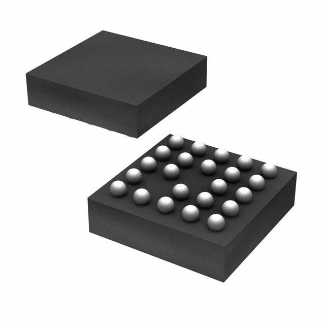
10) CSP 23pin Small and Thin package
●Applications
Flash and torch of camera for mobile phone
●Line up matrix
Parameter
BD6062GU
Input voltage
2.7 ~ 5.5V
Switching Frequency
480 ~ 720kHz
Maximum LED Current
1A
Package
VCSP85H2
●Absolute maximum ratings (Ta=25℃)
Parameter
Symbol
Ratings
Unit
VMAX
7
V
Pd
1100 *1
mW
Operating temperature range
Topr
-30~+85
℃
Storage temperature range
Tstg
-55~+150
℃
Maximum applied voltage
Power dissipation
Condition
VBAT, VIO
*1 50mm × 58mm × 1.75mm At glass epoxy board mounting. When it’s used by more than Ta=25℃, it’s reduced by 11mW/℃
●Recommended operating range (Ta= -30℃ ~ +85℃)
Parameter
Symbol
Ratings
Min.
Typ.
Max.
Unit
Condition
Power Supply Voltage
VDD
2.7
3.6
5.5
V
*2
IO Supply Voltage
VIO
1.62
1.8
3.3
V
*2
*2
VBAT ≥ VIO
www.rohm.com
© 2011 ROHM Co., Ltd. All rights reserved.
1/15
2011.05 - Rev.B
�Technical Note
BD6062GU
●Electrical characteristics
(Unless otherwise noted, Ta = +25℃, VBAT=3.6V, VIO=1.8V)
Limits
Parameter
Symbol
Min.
Typ.
Max.
Units
Condition
[Logic control terminal (IFMODE=’L’, 3wired control mode)]
Low threshold voltage1
VthL1
-
-
VIO* 0.25
V
High threshold voltage1
VthH1
VIO* 0.75
-
-
V
High level Input current1
IinH1
-
-
5
μA
Vin=VIO
Low level Input current1
IinL1
-5
-
-
μA
Vin=0V
[Logic control terminal (IFMODE=’H’, Direct control mode)]
Low threshold voltage2
VthL2
-
-
0.4
V
High threshold voltage2
VthH2
1.4
-
-
V
High level Input current2
IinH2
-
18.3
30
μA
FLASH=TORCH=5.5V
Low level Input current2
IinL2
-2
-0.1
-
μA
FLASH=TORCH=0V
Input voltage range
Vin
3.1
-
5.5
V
VBAT input range
Quiescent Current
Iq
-
5
10
μA
Torch=Flash= OFF
Current Consumption
Idd1
-
1.8
2.5
mA
VFB=1.0V, Vin=3.6V,
Torch mode
Inductor current limit
Icoil
1.5
2.0
2.5
A
Switching frequency
fSW
480
600
720
kHz
SW ON resistance
Ron
-
0.07
0.15
Ω
Iin=200mA
Duty cycle limit
Duty
60
65
-
%
VFB=0V
Output voltage range
Vo
-
-
5.4
V
Over voltage limit
Ovl
5.4
5.5
5.6
V
Start up time
Ts
0.5
1.0
ms
0mA to 200mA(Torch)
[Others]
Vin=3.6V *3
VFB=0V
R torch terminal voltage 1
Vrt1
45
50
55
mV
Itorch[1:0]=00 (50mA)
R torch terminal voltage 2
Vrt2
90
100
110
mV
Itorch[1:0]=01 (100mA)
R torch terminal voltage 3
Vrt3
135
150
165
mV
Itorch[1:0]=10 (150mA)
R torch terminal voltage 4
Vrt4
180
200
220
mV
Itorch[1:0]=11 (200mA)
R flash terminal voltage 1
Vrf1
43
48
53
mV
Iflash[1:0]=00 (400mA)
R flash terminal voltage 2
Vrf2
54
60
66
mV
Iflash[1:0]=01 (500mA)
R flash terminal voltage 3
Vrf3
65
72
79
mV
Iflash[1:0]=10 (600mA)
R flash terminal voltage 4
Vrf4
86
96
106
mV
Iflash[1:0]=11 (800mA)
*3 This parameter is tested with dc measurement.
www.rohm.com
© 2011 ROHM Co., Ltd. All rights reserved.
2/15
2011.05 - Rev.B
�Technical Note
BD6062GU
0.08
0.06
0.04
Ta=85°C
Ta=25°C
Ta=-30°C
0.02
0
3
0.08
0.06
0.04
(VBAT)
0
0
1.8
Ta=-30°C
1.2
0.6
2
VBAT=3.0V VBAT=2.7V
70
Fig.6 Switching Frequency
VBAT=3.6V
VBAT=4.2V
VBAT=3.0V
80
VBAT=2.7V
70
200 400 600 800 1000
LED CURRENT : ILED[mA]
85
Taiyo Yuden Coil
80
Panasonic Coil
75
EFFICIENCY [%]
TDK Coil
90
100
95
95
90
Taiyo Yuden Coil
85
TDK Coil
80
Panasonic Coil
200 400 600 800 1000
LED CURRENT : ILED[mA]
Fig.10 Each Coil Efficiency
(Ta = 25°C, VBAT = 3.6V)
www.rohm.com
© 2011 ROHM Co., Ltd. All rights reserved.
90
TDK Coil
85
Taiyo Yuden Coil
Panasonic Coil
80
75
70
0
200 400 600 800 1000
LED CURRENT : ILED[mA]
Fig.9 1A appli. Efficiency
(Ta = -30°C)
100
75
70
0
EFFICIENCY [%]
95
VBAT=2.7V
70
200 400 600 800 1000
LED CURRENT : ILED[mA]
Fig.8 1A appli. Efficiency
(Ta = 85°C)
100
VBAT=3.0V
50
0
Fig.7 1A appli. Efficiency
(Ta = 25°C)
80
VBAT=4.2V
60
50
0
VBAT=3.6V
90
60
50
2.5 3 3.5 4 4.5 5 5.5
INPUT VOLTAGE : VBAT[V]
100
90
60
Ta=-30°C
2
EFFICIENCY [%]
80
VBAT=4.2V
Ta=25°C
500
3.5
4
4.5
5
5.5
INPUT VOLTAGE : VBAT[V]
Fig.5 Over-Current Limiter
EFFICIENCY [%]
VBAT=3.6V
Ta=85°C
550
100
90
EFFICIENCY [%]
Ta=-30°C
3
100
1
2
3
4
5
INPUT VOLTAGE : VBAT[V]
600
Ta=85°C
1.75
Fig.4 Current consumption(VBAT)
0
650
Ta=25°C
7
Ta=85°C
Ta=25°C
Ta=-30°C
0.02
700
1.5
1
2
3
4
5
6
INPUT VOLTAGE : VBAT[V]
0.04
Fig.3 Quiescent current consumption
(OVP)
2.25
0
0.06
SWITCHING FREQUENCY :
FSW[kHz]
CURRENT LIMIT : llimit[A]
Ta=85°C
Ta=25°C
0.08
0
2.5
2.4
0.1
1
2
3
4
5
INPUT VOLTAGE : VBAT[V]
Fig.2 Quiescent current consumption
(VIO)
3
0
EFFICIENCY [%]
Ta=85°C
Ta=25°C
Ta=-30°C
0.02
3.5
4
4.5
5
5.5
INPUT VOLTAGE : VBAT[V]
Fig.1 Quiescent current consumption
CURRENT CONSUMPTION: ldd[mA]
0.1
STAND-BY CURRENT: lstb_VIO[μA]
STAND-BY CURRENT : lstb[μA]
0.1
STAND-BY CURRENT : lstb_OVP[μA]
●Electrical characteristic curves (Reference data)
70
0
200 400 600 800 1000
LED CURRENT : ILED[mA]
Fig.11 Each Coil Efficiency
(Ta = 85°C, VBAT = 3.6V)
3/15
0
200 400 600 800 1000
LED CURRENT : ILED[mA]
Fig.12 Each Coil Efficiency
(Ta = -30°C, VBAT = 3.6V)
2011.05 - Rev.B
�Technical Note
BD6062GU
●Electrical characteristic curves (Reference data) – Continued
0.22
0.2
0.19
0.18
Ta=85°C
Ta=25°C
Ta=-30°C
0.21
0.2
0.19
0.18
0
50
100 150 200 250
TFB CURRENT : ITFB[mA]
Fig.13 TORCH Load Regulation
(VBAT = 5.5V)
Ta=85°C
90
85
80
100
95
Ta=-30°C
90
Ta=85°C
Ta=25°C
85
80
0
300
600
900
1200
FFB CURRENT : IFFB[mA]
Fig.16 FLASH Load Regulation
(VBAT = 5.5V)
50
100 150 200 250
TFB CURRENT : ITFB[mA]
Fig.15 TORCH Load Regulation
(VBAT = 2.7V)
FFB VOLTAGE: VFFB[mV]
Ta=25°C
0.19
0
Fig.14 TORCH Load Regulation
(VBAT = 3.6V)
FFB VOLTAGE: VFFB[mV]
Ta=-30°C
0.2
50
100 150 200 250
TFB CURRENT : ITFB[mA]
100
95
Ta=85°C
Ta=25°C
Ta=-30°C
0.21
0.18
0
100
FFB VOLTAGE : VFFB[mV]
0.22
TFB VOLTAGE: VTFB[V]
Ta=85°C
Ta=25°C
Ta=-30°C
0.21
TFB VOLTAGE: VTFB[V]
TFB VOLTAGE : VTFB[V]
0.22
Ta=85°C
95
Ta=-30°C Ta=25°C
90
85
80
0
300
600
900
1200
FFB CURRENT : IFFB[mA]
0
Fig.17 FLASH Load Regulation
(VBAT = 3.6V)
300
600
900
1200
TFB CURRENT : ITFB[mA]
Fig.18 FLASH Load Regulation
(VBAT = 2.7V)
TORCH/FLASH Terminal
(VBAT) [500mV/div]
OUTPUT VOLTAGE [500mV/div]
OUTPUT VOLTAGE
[500mV/div]
TORCH/FLASH Terminal
(VBAT) [500mV/div]
TORCH/FLASH Terminal
(VBAT) [1V/div]
INPUT CURRENT [200mA/div]
LED CURRENT
[200mA/div]
0V, 0A
200µs/div
Fig.19 500mA Input rush current
(VBAT=3.0V)
0V, 0A
INPUT CURRENT
[200mA/div]
OUTPUT VOLTAGE [1A/div]
LED CURRENT
[200mA/div]
LED CURRENT [200mA/div]
200µs/div
Fig.20 500mA Input rush current
(VBAT=3.6V)
INPUT CURRENT [200mA/div]
0V, 0A
200µs/div
Fig.21 500mA Input rush current
(VBAT=4.5V)
OUTPUT VOLTAGE [500mV/div]
TORCH/FLASH Terminal
(VBAT) 500mV/div]
LED CURRENT
[200mA/div]
INPUT CURRENT
[500mA/div]
Fig.22 1A Input rush current
(200mA 1A)
www.rohm.com
© 2011 ROHM Co., Ltd. All rights reserved.
4/15
2011.05 - Rev.B
�Technical Note
BD6062GU
●Block diagram and pin configuration
VBAT
Battery
2.2µF
VBAT
GND
GND
VIO
VIO
4.7µH
4.7µH
SBD
SBD
SW1
SW1
osc
R
Q
S
Q
47µF
(6.3V)
SW2
osc
R
Q
S
Q
47µF
PGND1
CLK
slope
PGND2
CURDRV
TORCH
TORCH (CS)
CURDRV
FLASH
VFB
RFLASH
RFLASH
FFB
Control
CURDRV
TORCH
TORCH (CS)
OVP
FFB
Control
TFB
1Ω
CURDRV
FLASH
RTORCH
CLK
CSDI
IFMODE
PGND2
VFB
RTORCH
FLASH
(RSTB)
TFB
CSDI
0.12Ω
GNDSENS
RSTB
(FLASH)
OVP
IFMODE
1Ω
0.12Ω
GNDSENS
OVP
OVP
TEST
TEST
OPEN
OPEN
Fig.24 1A application Block diagram of
3wired control Mode
Fig.23 1A application Block diagram of
Direct control Mode
VBAT
Battery
4.7µF
VBAT
(6.3V)
GND
VIO
VIO
4.7µH
4.7µH
SBD
SBD
SW1
osc
R
Q
S
Q
SW1
22µF
(6.3V)
SW2
osc
R
Q
S
Q
PGND1
slope
PGND2
VFB
RFLASH
CURDRV
TORCH
CURDRV
FLASH
RFLASH
FFB
CURDRV
TORCH
TORCH (CS)
RTORCH
Control
Control
TFB
2Ω
IFMODE
OVP
CURDRV
FLASH
FFB
RTORCH
CLK
CSDI
FLASH
(RSTB)
22µF
(6.3V)
SW2
PGND1
slope
PGND2
VFB
TORCH (CS)
Battery
4.7µF
(6.3V)
GND
CLK
(6.3V)
SW2
PGND1
slope
Battery
2.2µF
(6.3V)
(6.3V)
TFB
CSDI
0.24Ω
GNDSENS
FLASH
(RSTB)
OVP
IFMODE
2Ω
OVP
TEST
0.24Ω
GNDSENS
OVP
TEST
OPEN
OPEN
Fig.25 500mA application Block diagram of
Direct control Mode
A
Fig.26 500mA application Block diagram of
3wired control Mode
B
C
D
E
5
N.C.
SW2
VIO
PGND2
N.C.
4
GND
SENS
SW1
CSDI
PGND1
CLK
3
FTB
IFMODE
OVP
VBAT
2
RSTB/
FLASH
TFB
CS/
TORCH
GND
1
TEST
VFB
RTORCH
N.C.
RFLASH
Fig.27 pin location diagram (TOP VIEW)
www.rohm.com
© 2011 ROHM Co., Ltd. All rights reserved.
5/15
2011.05 - Rev.B
�Technical Note
BD6062GU
●Pin assignment table
No.
Pin Name
A1
TEST
In/
Out
In
A2
RSTB/FLASH
In
A3
A4
A5
B1
B3
B4
B5
C1
C2
C4
C5
D1
FFB
GNDSENS
N.C
RFLASH
IFMODE
SW1
SW2
VFB
TFB
CSDI
VIO
RTORCH
In
In
Out
In
In
In
In
In
In
Out
D2
CS/TORCH
In
D3
D4
D5
E1
E2
E3
E4
E5
OVP
PGND1
PGND2
N.C
GND
In
In
-
VBAT
CLK
N.C
Functions
Digital test select pin
Reset (“L”:Reset) (IFMODE=’0’)
FLASH enable (“H”) (IFMODE=’1’)
Flash current driver feedback pin
Sense GND pin for current driver
open
Flash current adjustment resistor pin
Interface mode select
Switching terminal 1
Switching terminal 2
Voltage feedback pin
Torch current driver feedback pin
Data input
I/O power supply pin
Torch current adjustment resistor pin
Chip select
(IFMODE=’0’)
TORCH enable (IFMODE=’1’)
Boost voltage feedback input pin
Power GND pin 1
Power GND pin 2
Open
GND pin
Battery power supply pin
Clock
Open
Total : 23 Pin
●Description of function
1) CPU I/F
The Control Serial I/F provides access to Flash LED driver control registers.
Write timing show following timing chart.
CLK
Duty
tsFS thFS
Tcyc
CS
tsDI
CSDI
thDI
A7
A6
A0
D7
D6
D0
Fig.28 Control Serial Port Timing
www.rohm.com
© 2011 ROHM Co., Ltd. All rights reserved.
6/15
2011.05 - Rev.B
�Technical Note
BD6062GU
Control Serial Port Specifications
Limits
Symbol
Parameter
Min.
Typ.
Max.
Unit
CS Input Setup
tsFS
50
-
-
ns
CS Input Hold
thFS
50
-
-
ns
CSDI Input Setup
tsDI
50
-
-
ns
CSDI Input Hold
thDI
50
-
-
ns
Clock Cycle Time
Tcyc
133.3
-
-
ns
Duty Ratio
Duty
40
50
60
%
Condition
MAX 7.5 MHz
Performance specifications are guaranteed, but not production tested.
2) Register map
ENA
Address
[7:0]
01 (H)
-
-
-
-
-
-
Flash
Torch
TIME
02 (H)
-
Tmode
Tdelay2
Tdelay1
Tdelay0
Tflash2
Tflash1
Tflash0
CURR
03 (H)
-
-
-
CLMT
Iflash1
Iflash0
Itorch1
Itorch0
TEST
04 (H)
-
-
-
-
Test3
Test2
Test1
Test0
TEST2
05 (H)
-
-
-
TEST24
TEST23
TEST22
TEST21
TEST20
Symbol
D[7]
D[6]
D[5]
D[4]
D[3]
D[2]
D[1]
D[0]
*Note: Write access is prohibited in TEST and TEST2 registers.
Address”00(H)”, Enable control
2-1) Enable control
Flash
Torch
Output
Default
*
0
0
off
0
1
Itorch
1
0
Iflash
1
1
Itorch + Iflash
*When IFMODE=H, each enable signal are controlled by CPU directly from Pin.
Address”01(H)”, Timer mode setting and Flash timer period control
2-2) Timer mode control
Tmode
Timer mode
Default
0
disable
1
enable
www.rohm.com
© 2011 ROHM Co., Ltd. All rights reserved.
*
7/15
2011.05 - Rev.B
�Technical Note
BD6062GU
2-3) Flash delay timer setting
Tdelay[2:0]
tFlash1
000
0ms
001
5ms
010
10ms
011
15ms
100
20ms
101
25ms
110
30ms
111
35ms
Default
*
tFLASH1 : Flash on delay timer
It control the period from flash enable to
light up.
2-4) Flash ON timer setting
Tflash[2:0]
TFlash2
000
50ms
001
100ms
010
150ms
011
200ms
100
400ms
101
600ms
110
800ms
111
1000ms
tFLASH2 : Flash on timer
It control the period from light up to off.
Default
*
*When IFMODE=H, it does not use timer function. Flash period is controlled by CPU directly.
Address”02(H)”, Flash and Torch current setting
2-5) Output current setting for the Torch current driver
Itorch[1:0]
Output current
Default
00
50mA
*
01
100mA
10
150mA
11
200mA
2-6) Output current setting for the Flash current driver
Iflash[1:0]
Output current
Default
00
400mA
*
01
500mA
10
600mA
11
800mA
2-7) Over power protection enable
CLMT
Current Limit
0
disable
1
enable
www.rohm.com
© 2011 ROHM Co., Ltd. All rights reserved.
Default
*
IFMODE=H
*
IFMODE=H
*
IFMODE=H
*
8/15
2011.05 - Rev.B
�Technical Note
BD6062GU
It depends on battery or external components condition, internal power consumption will be large at flash action and there is
a possibility that it will over Power dissipation of IC.
BD6062GU can limit drive current on over power condition, and protect to over Power dissipation.
When this mode is enable, BD6062GU limit maximum current automatically as below.
Torch
Flash
Max200mA
Max800mA
Max200mA
400mA
3) Power Control
BD6062GU can be controlled the status of activation using Enable control resistor.
4) LED drive current (Torch Mode)
The LED current is decided by the voltage of RTORCH terminal. (Rtorch=1.0Ω)
ILED is given as follows,
ILED= I(Torch Current Driver)=VRTORCH / 1.0(Ω)
Rtorch =1.0Ω, ILED=50mA
: Itorch [1:0] = 00
VRTORCH =0.05V,
VRTORCH =0.2V,
Rtorch =1.0Ω, ILED=200mA : Itorch [1:0] = 11
VRTORCH is controlled 0.05V~0.2V by resistor setting.
5) LED drive current (Flash Mode)
The LED current is decided by the voltage of RFLASH terminal and RTORCH terminal.
(Rflash=0.12Ω, Rtorch=1.0Ω)
ILED is given as follows,
ILED= I(Flash Current Driver)+I(Torch Current Driver) =VRFLASH/0.12(Ω)+VRTORCH / 1.0(Ω)
VRFLASH=0.096V,
Rflash =0.12Ω,
Itorch[1:0]=11
ILED=200mA+800mA=1000mA
VRTORCH=0.2V,
Rtorch =1.0Ω,
Iflash[1:0]=11
VRFLASH is controlled 0.048V~0.096V by resistor setting.
6) Basic function
i) Register control interface(3wired) mode (timer enable)
Torch
(Address : 00 (H), D[0])
Flash
(Address : 00 (H), D[1])
tFLASH1
tFLASH2
ILED2
ILED
(0mA)
ILED1
ILED1 : Torch Current Driver
ILED2 : Forch Current Driver
tFLASH1,2 : Flash time is controlled by timer resistor setting.
Fig.29 3wired mode Torch and Flash Timing (Timer enable)
www.rohm.com
© 2011 ROHM Co., Ltd. All rights reserved.
9/15
2011.05 - Rev.B
�Technical Note
BD6062GU
ii) Register control interface(3wired) mode (timer disable)
Torch
(Address : 00 (H), D[0])
Flash
(Address : 00 (H), D[1])
tFLASH2
ILED2
ILED
(0mA)
ILED1
ILED1 : Torch Current Driver
ILED2 : Flash Current Driver
tFLASH2
: Flash period protect
Fig.30 3wired mode Torch and Flash Timing (Timer disable)
If flash period is over tFLASH2 setting, flash current driver will enable to turn off.
Protect time is controlled by flash ON timer resister setting.
iii) Direct control interface mode
TORCH (Pin)
FLASH (Pin)
500ms
800mA
ILED
(0mA)
200mA
There is LED protect function in this mode.
Flash period is over 500ms, then this mode turn off flash.
Fig.31 Direct Control mode Torch and Flash Timing
iv) The voltage of VFB is as follows, (in DC/DC on)
Torch mode 350mV
Flash mode 350mV
www.rohm.com
© 2011 ROHM Co., Ltd. All rights reserved.
10/15
2011.05 - Rev.B
�Technical Note
BD6062GU
7) Soft start
BD6062GU has soft start function.
Soft start function will prevent the big peak current from IC and coil.
The detail of soft start is as follows.
L
A
ERRAMP
VOUT
SW
B
R
Q
S
Q
C
PGND
OSC
EN
VOUT
A
B (dashed)
C
duty width increase little by little
Fig.32 Soft start Diagram and Timing
8) Soft Current Limiter
BD6062GU has Soft Current Limiter function.
Soft current limiter function will change the value of current gradually.
It has four steps. And the steps are as follows;
4Step of soft current limiter
Action
Time
Current Limit (DC)
Current Limit “H (peak)
Current Limit “L (peak)
Start
0~500us
0A* always
1.125A
0.675A
2nd step
500~700us
0.5A
1.75A
1.05A
3rd step
700~800us
1A
2.375A
1.425A
4th step
800~900us
1.5A
3.0A
1.8A
Normal
900us~
2A
3.625A
2.175A
Peak current of BD6062GU depends on only soft current limiter.
Switching frequency or VBAT voltage does not affect Peak current of BD6062GU.
9) Thermal shut down
BD6062GU has a thermal shut down function.
It works above 175℃, and while, IC will change the status from active to inactive.
When the temperature will be under 175℃, IC will return to normal operation.
www.rohm.com
© 2011 ROHM Co., Ltd. All rights reserved.
11/15
2011.05 - Rev.B
�Technical Note
BD6062GU
10) Safety functions
10-1) Over voltage detect function (OVP)
When OVP become more than 5.5V, IC stop the switching.
When OVP become less than detect voltage, the status of switching will restart.
10-2) Open detect function (ODF)
When OVP pin is not connected any components, IC will stop the switching.
Absolute voltage
stop the switching
5.5V(typ)
OVP
Normal operation
normal voltage
0.7V(typ)
stop the switching
OPEN
0V
Fig.33 Safety Voltage range
●Selection of external parts
Recommended external parts are as shown below.
When to use other parts than these, select the following equivalent parts.
Coil(L1)
Size
Value
Vendor
Parts number
X
Y
Z
DCR
(ohm)
4.7μH
Taiyou Yuden
NR4018T4R7M
4.0
4.0
1.8
0.09
4.7μH
TDK
VLF3012AT-4R7MR74*
2.6
2.8
1.2
0.13
*) for under 500mA application
Capacitor
Value
Vendor
Parts number
MURATA
47μF
22μF
Size
X
Y
Z
GRM188B30J225KE
1.6
0.8
0.8
MURATA
GRM32EB31A476KE20
3.2
3.2
2.5
MURATA
GRM21BB30J226ME38B*
2.0
1.25
1.25
Cin
2.2μF
Cout
*) for under 500mA application
Resistance
Value
Vendor
Parts number
Size
X
Y
Z
class
Rflash
0.12ohm
ROHM
MCR10EZHFLR120
2.0
1.25
0.55
±1%
0.24ohm
ROHM
MCR10EZHFLR240*
2.0
1.25
0.55
±1%
Rtorch
1.0ohm
ROHM
MCR10EZHFL1R00
2.0
1.25
0.55
±1%
2.0ohm
ROHM
MCR10EZHFL2R00*
2.0
1.25
0.55
±1%
*) for under 500mA application
Shotkey Diode(D1)
VF
Vendor
Parts number
0.43V
ROHM
RB160M-30
www.rohm.com
© 2011 ROHM Co., Ltd. All rights reserved.
12/15
Size
X
Y
Z
2.6
1.6
0.80
2011.05 - Rev.B
�Technical Note
BD6062GU
●Recommended layout pattern
BD6062GU
+
R2
D1
L1
+
LED
COUT
A1
R1
CIN
GND
VBAT
Fig.34 Frontal surface (TOP VIEW)
Fig.35 Middle surface1 (TOP VIEW)
Fig.36 Middle surface2 (TOP VIEW)
Fig.37 Rear surface (TOP VIEW)
●Notes for use
( 1 ) Absolute Maximum Ratings
An excess in the absolute maximum ratings, such as supply voltage, temperature range of operating conditions, etc.,
can break down devices, thus making impossible to identify breaking mode such as a short circuit or an open circuit. If
any special mode exceeding the absolute maximum ratings is assumed, consideration should be given to take physical
safety measures including the use of fuses, etc.
(2)
Operating conditions
These conditions represent a range within which characteristics can be provided approximately as expected. The
electrical characteristics are guaranteed under the conditions of each parameter.
(3)
Reverse connection of power supply connector
The reverse connection of power supply connector can break down ICs. Take protective measures against the
breakdown due to the reverse connection, such as mounting an external diode between the power supply and the IC’s
power supply terminal.
(4)
Power supply line
Design PCB pattern to provide low impedance for the wiring between the power supply and the GND lines. In this
regard, for the digital block power supply and the analog block power supply, even though these power supplies has
the same level of potential, separate the power supply pattern for the digital block from that for the analog block, thus
suppressing the diffraction of digital noises to the analog block power supply resulting from impedance common to the
wiring patterns. For the GND line, give consideration to design the patterns in a similar manner.
Furthermore, for all power supply terminals to ICs, mount a capacitor between the power supply and the GND terminal.
At the same time, in order to use an electrolytic capacitor, thoroughly check to be sure the characteristics of the
capacitor to be used present no problem including the occurrence of capacity dropout at a low temperature, thus
determining the constant.
(5)
GND voltage
Make setting of the potential of the GND terminal so that it will be maintained at the minimum in any operating state.
Furthermore, check to be sure no terminals are at a potential lower than the GND voltage including an actual electric
transient.
www.rohm.com
© 2011 ROHM Co., Ltd. All rights reserved.
13/15
2011.05 - Rev.B
�Technical Note
BD6062GU
(6)
Short circuit between terminals and erroneous mounting
In order to mount ICs on a set PCB, pay thorough attention to the direction and offset of the ICs. Erroneous mounting
can break down the ICs. Furthermore, if a short circuit occurs due to foreign matters entering between terminals or
between the terminal and the power supply or the GND terminal, the ICs can break down.
(7)
Operation in strong electromagnetic field
Be noted that using ICs in the strong electromagnetic field can malfunction them.
(8)
Inspection with set PCB
On the inspection with the set PCB, if a capacitor is connected to a low-impedance IC terminal, the IC can suffer stress.
Therefore, be sure to discharge from the set PCB by each process. Furthermore, in order to mount or dismount the set
PCB to/from the jig for the inspection process, be sure to turn OFF the power supply and then mount the set PCB to
the jig. After the completion of the inspection, be sure to turn OFF the power supply and then dismount it from the jig. In
addition, for protection against static electricity, establish a ground for the assembly process and pay thorough attention
to the transportation and the storage of the set PCB.
(9)
Input terminals
In terms of the construction of IC, parasitic elements are inevitably formed in relation to potential. The operation of the
parasitic element can cause interference with circuit operation, thus resulting in a malfunction and then breakdown of
the input terminal. Therefore, pay thorough attention not to handle the input terminals, such as to apply to the input
terminals a voltage lower than the GND respectively, so that any parasitic element will operate. Furthermore, do not
apply a voltage to the input terminals when no power supply voltage is applied to the IC. In addition, even if the power
supply voltage is applied, apply to the input terminals a voltage lower than the power supply voltage or within the
guaranteed value of electrical characteristics.
( 10 ) Ground wiring pattern
If small-signal GND and large-current GND are provided, It will be recommended to separate the large-current GND
pattern from the small-signal GND pattern and establish a single ground at the reference point of the set PCB so that
resistance to the wiring pattern and voltage fluctuations due to a large current will cause no fluctuations in voltages of
the small-signal GND. Pay attention not to cause fluctuations in the GND wiring pattern of external parts as well.
( 11 ) External capacitor
In order to use a ceramic capacitor as the external capacitor, determine the constant with consideration given to a
degradation in the nominal capacitance due to DC bias and changes in the capacitance due to temperature, etc.
( 12 ) Thermal shutdown circuit (TSD)
When junction temperatures become 175℃ (typ) or higher, the thermal shutdown circuit operates and turns a switch
OFF. The thermal shutdown circuit, which is aimed at isolating the LSI from thermal runaway as much as possible, is
not aimed at the protection or guarantee of the LSI. Therefore, do not continuously use the LSI with this circuit
operating or use the LSI assuming its operation.
( 13 ) Thermal design
Perform thermal design in which there are adequate margins by taking into account the permissible dissipation (Pd) in
actual states of use.
( 14 ) Selection of coil
Select the low DCR inductors to decrease power loss for DC/DC converter.
www.rohm.com
© 2011 ROHM Co., Ltd. All rights reserved.
14/15
2011.05 - Rev.B
�Technical Note
BD6062GU
●Ordering part number
B
D
6
Part No.
0
6
2
G
Part No.
6062
U
-
E
Package
GU : VCSP85H2
2
Packaging and forming specification
E2: Embossed tape and reel
VCSP85H2 (BD6062GU)
2.86±0.1
1.0MAX
0.25± 0.1
2.86± 0.1
1PIN MARK
(φ0.15)INDEX POST
B
1
0.43±0.1
E2
The direction is the 1pin of product is at the upper left when you hold
( reel on the left hand and you pull out the tape on the right hand
)
0.43± 0.1
A
E
D
C
B
A
2500pcs
P=0.5 × 4
0.08 S
0.05 A B
Embossed carrier tape
Quantity
Direction
of feed
S
23- φ 0.30±0.05
Tape
2 3 4 5
1pin
P=0.5×4
Reel
(Unit : mm)
www.rohm.com
© 2011 ROHM Co., Ltd. All rights reserved.
15/15
Direction of feed
∗ Order quantity needs to be multiple of the minimum quantity.
2011.05 - Rev.B
�Datasheet
Notice
Precaution on using ROHM Products
1.
Our Products are designed and manufactured for application in ordinary electronic equipments (such as AV equipment,
OA equipment, telecommunication equipment, home electronic appliances, amusement equipment, etc.). If you
(Note 1)
, transport
intend to use our Products in devices requiring extremely high reliability (such as medical equipment
equipment, traffic equipment, aircraft/spacecraft, nuclear power controllers, fuel controllers, car equipment including car
accessories, safety devices, etc.) and whose malfunction or failure may cause loss of human life, bodily injury or
serious damage to property (“Specific Applications”), please consult with the ROHM sales representative in advance.
Unless otherwise agreed in writing by ROHM in advance, ROHM shall not be in any way responsible or liable for any
damages, expenses or losses incurred by you or third parties arising from the use of any ROHM’s Products for Specific
Applications.
(Note1) Medical Equipment Classification of the Specific Applications
JAPAN
USA
EU
CHINA
CLASSⅢ
CLASSⅡb
CLASSⅢ
CLASSⅢ
CLASSⅣ
CLASSⅢ
2.
ROHM designs and manufactures its Products subject to strict quality control system. However, semiconductor
products can fail or malfunction at a certain rate. Please be sure to implement, at your own responsibilities, adequate
safety measures including but not limited to fail-safe design against the physical injury, damage to any property, which
a failure or malfunction of our Products may cause. The following are examples of safety measures:
[a] Installation of protection circuits or other protective devices to improve system safety
[b] Installation of redundant circuits to reduce the impact of single or multiple circuit failure
3.
Our Products are designed and manufactured for use under standard conditions and not under any special or
extraordinary environments or conditions, as exemplified below. Accordingly, ROHM shall not be in any way
responsible or liable for any damages, expenses or losses arising from the use of any ROHM’s Products under any
special or extraordinary environments or conditions. If you intend to use our Products under any special or
extraordinary environments or conditions (as exemplified below), your independent verification and confirmation of
product performance, reliability, etc, prior to use, must be necessary:
[a] Use of our Products in any types of liquid, including water, oils, chemicals, and organic solvents
[b] Use of our Products outdoors or in places where the Products are exposed to direct sunlight or dust
[c] Use of our Products in places where the Products are exposed to sea wind or corrosive gases, including Cl2,
H2S, NH3, SO2, and NO2
[d] Use of our Products in places where the Products are exposed to static electricity or electromagnetic waves
[e] Use of our Products in proximity to heat-producing components, plastic cords, or other flammable items
[f] Sealing or coating our Products with resin or other coating materials
[g] Use of our Products without cleaning residue of flux (even if you use no-clean type fluxes, cleaning residue of
flux is recommended); or Washing our Products by using water or water-soluble cleaning agents for cleaning
residue after soldering
[h] Use of the Products in places subject to dew condensation
4.
The Products are not subject to radiation-proof design.
5.
Please verify and confirm characteristics of the final or mounted products in using the Products.
6.
In particular, if a transient load (a large amount of load applied in a short period of time, such as pulse. is applied,
confirmation of performance characteristics after on-board mounting is strongly recommended. Avoid applying power
exceeding normal rated power; exceeding the power rating under steady-state loading condition may negatively affect
product performance and reliability.
7.
De-rate Power Dissipation (Pd) depending on Ambient temperature (Ta). When used in sealed area, confirm the actual
ambient temperature.
8.
Confirm that operation temperature is within the specified range described in the product specification.
9.
ROHM shall not be in any way responsible or liable for failure induced under deviant condition from what is defined in
this document.
Precaution for Mounting / Circuit board design
1.
When a highly active halogenous (chlorine, bromine, etc.) flux is used, the residue of flux may negatively affect product
performance and reliability.
2.
In principle, the reflow soldering method must be used; if flow soldering method is preferred, please consult with the
ROHM representative in advance.
For details, please refer to ROHM Mounting specification
Notice - GE
© 2014 ROHM Co., Ltd. All rights reserved.
Rev.002
�Datasheet
Precautions Regarding Application Examples and External Circuits
1.
If change is made to the constant of an external circuit, please allow a sufficient margin considering variations of the
characteristics of the Products and external components, including transient characteristics, as well as static
characteristics.
2.
You agree that application notes, reference designs, and associated data and information contained in this document
are presented only as guidance for Products use. Therefore, in case you use such information, you are solely
responsible for it and you must exercise your own independent verification and judgment in the use of such information
contained in this document. ROHM shall not be in any way responsible or liable for any damages, expenses or losses
incurred by you or third parties arising from the use of such information.
Precaution for Electrostatic
This Product is electrostatic sensitive product, which may be damaged due to electrostatic discharge. Please take proper
caution in your manufacturing process and storage so that voltage exceeding the Products maximum rating will not be
applied to Products. Please take special care under dry condition (e.g. Grounding of human body / equipment / solder iron,
isolation from charged objects, setting of Ionizer, friction prevention and temperature / humidity control).
Precaution for Storage / Transportation
1.
Product performance and soldered connections may deteriorate if the Products are stored in the places where:
[a] the Products are exposed to sea winds or corrosive gases, including Cl2, H2S, NH3, SO2, and NO2
[b] the temperature or humidity exceeds those recommended by ROHM
[c] the Products are exposed to direct sunshine or condensation
[d] the Products are exposed to high Electrostatic
2.
Even under ROHM recommended storage condition, solderability of products out of recommended storage time period
may be degraded. It is strongly recommended to confirm solderability before using Products of which storage time is
exceeding the recommended storage time period.
3.
Store / transport cartons in the correct direction, which is indicated on a carton with a symbol. Otherwise bent leads
may occur due to excessive stress applied when dropping of a carton.
4.
Use Products within the specified time after opening a humidity barrier bag. Baking is required before using Products of
which storage time is exceeding the recommended storage time period.
Precaution for Product Label
QR code printed on ROHM Products label is for ROHM’s internal use only.
Precaution for Disposition
When disposing Products please dispose them properly using an authorized industry waste company.
Precaution for Foreign Exchange and Foreign Trade act
Since our Products might fall under controlled goods prescribed by the applicable foreign exchange and foreign trade act,
please consult with ROHM representative in case of export.
Precaution Regarding Intellectual Property Rights
1.
All information and data including but not limited to application example contained in this document is for reference
only. ROHM does not warrant that foregoing information or data will not infringe any intellectual property rights or any
other rights of any third party regarding such information or data. ROHM shall not be in any way responsible or liable
for infringement of any intellectual property rights or other damages arising from use of such information or data.:
2.
No license, expressly or implied, is granted hereby under any intellectual property rights or other rights of ROHM or any
third parties with respect to the information contained in this document.
Other Precaution
1.
This document may not be reprinted or reproduced, in whole or in part, without prior written consent of ROHM.
2.
The Products may not be disassembled, converted, modified, reproduced or otherwise changed without prior written
consent of ROHM.
3.
In no event shall you use in any way whatsoever the Products and the related technical information contained in the
Products or this document for any military purposes, including but not limited to, the development of mass-destruction
weapons.
4.
The proper names of companies or products described in this document are trademarks or registered trademarks of
ROHM, its affiliated companies or third parties.
Notice - GE
© 2014 ROHM Co., Ltd. All rights reserved.
Rev.002
�Datasheet
General Precaution
1. Before you use our Pro ducts, you are requested to care fully read this document and fully understand its contents.
ROHM shall n ot be in an y way responsible or liabl e for fa ilure, malfunction or acci dent arising from the use of a ny
ROHM’s Products against warning, caution or note contained in this document.
2. All information contained in this docume nt is current as of the issuing date and subj ect to change without any prior
notice. Before purchasing or using ROHM’s Products, please confirm the la test information with a ROHM sale s
representative.
3.
The information contained in this doc ument is provi ded on an “as is” basis and ROHM does not warrant that all
information contained in this document is accurate an d/or error-free. ROHM shall not be in an y way responsible or
liable for an y damages, expenses or losses incurred b y you or third parties resulting from inaccur acy or errors of or
concerning such information.
Notice – WE
© 2014 ROHM Co., Ltd. All rights reserved.
Rev.001
�


 工商网监
湘ICP备2023018690号
工商网监
湘ICP备2023018690号
