Datasheet
DC Brushless Fan Motor Driver
Multifunction Single-phase Full-wave
Fan Motor Driver
BD61250MUV
General Description
BD61250MUV is pre-driver IC to drive single phase H bridge output composed of external MOS FET.
The power supply input terminal and the drive output have voltage rating of 40V, so it can be used in a 24V power supply
without using voltage drop down circuit.
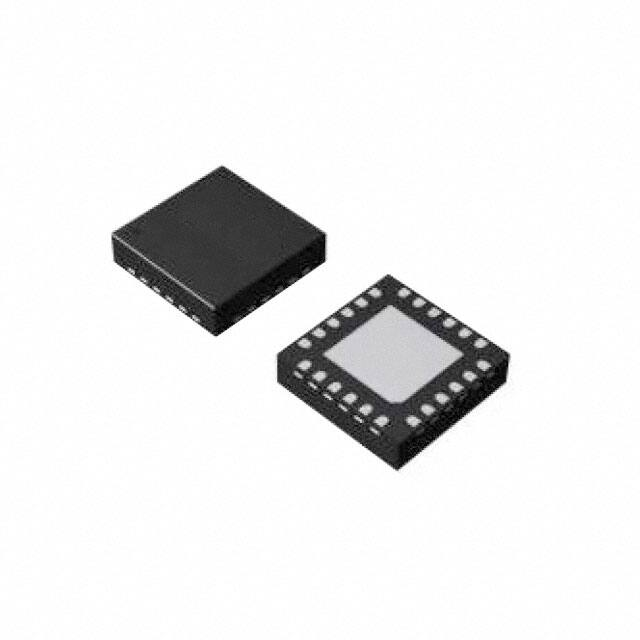
Package
Features
� Pre driver for external power MOS FET
� Speed controllable by PWM / DC voltage
� Minimum output duty limit
� Input / output duty slope adjustment
� Silent drive by the PWM soft switching
� Lead angle setting
� Soft start
� Standby mode
� Current limit
� Lock protection and automatic restart
� Rotation speed pulse signal(FG), Lock alarm
signal(AL) selectable
� Drive PWM frequency selectable (50kHz/25kHz)
VQFN024V4040
Application
� General consumer equipment of Desktop PC, Server,
etc.
� Office equipment, Copier, FAX, Laser Printer, etc.
Absolute Maximum Ratings
Parameter
Supply Voltage
Power Dissipation
Operating Temperature Range
Storage Temperature Range
Maximum Junction Temperature
High Side Output Voltage
Low Side Output Voltage
Output Current
Signal Output Voltage
Signal Output Current
Reference Voltage (REF) Output Current
Input Voltage1 (PWMIN, CS, FSEL, SSEL, STBEN)
Input Voltage2 (HP, HM, ADC input terminal)
Symbol
VCC
Pd
Topr
Tstr
Tjmax
VOH
VOL
IOMAX
VSIG
ISIG
IREF
VIN1
VIN2
W (Typ) x D (Typ) x H (Max)
4.00mm x 4.00mm x 1.00mm
VQFN024V4040
Rating
40
0.83(Note 1)
-40 to +105
-55 to +150
+150
VCC-7 to VCC
0 to 7
10
40
10
10
5.3
3.3
Unit
V
W
°C
°C
°C
V
V
mA
V
mA
mA
V
V
(Note 1) Derate by 6.64mW/°C when operating above Ta=25°C. (Mounted on 114.3mm×76.2mm×1.57mm 1layer board)
Caution 1: Operating the IC over the absolute maximum ratings may damage the IC. The damage can either be a short circuit between pins or an open circuit
between pins and the internal circuitry. Therefore, it is important to consider circuit protection measures, such as adding a fuse, in case the IC is
operated over the absolute maximum ratings.
Caution 2: Should by any chance the maximum junction temperature rating be exceeded the rise in temperature of the chip may result in deterioration of the
properties of the chip. In case of exceeding this absolute maximum rating, design a PCB boards with power dissipation and thermal resistance
taken into consideration by increasing board size and copper area so as not to exceed the maximum junction temperature rating.
○Product structure:Silicon monolithic integrated circuit ○This product has no designed protection against radioactive rays
www.rohm.com
TSZ02201-0H1H0B101660-1-2
© 2016 ROHM Co., Ltd. All rights reserved.
1/26
TSZ22111・14・001
20.Jul.2017 Rev.003
�Datasheet
BD61250MUV
Thermal Resistance(Note 1)
Parameter
Thermal Resistance (Typ)
Symbol
1s(Note 3)
2s2p(Note 4)
Unit
VQFN024V4040
Junction to Ambient
θJA
150.6
37.9
°C/W
Junction to Top Characterization Parameter(Note 2)
ΨJT
20
9
°C/W
(Note 1)Based on JESD51-2A(Still-Air)
(Note 2)The thermal characterization parameter to report the difference between junction temperature and the temperature at the top center of the outside
surface of the component package.
(Note 3)Using a PCB board based on JESD51-3.
Layer Number of
Measurement Board
Single
Material
Board Size
FR-4
114.3mm x 76.2mm x 1.57mmt
Top
Copper Pattern
Thickness
Footprints and Traces
70µm
(Note 4)Using a PCB board based on JESD51-7.
Layer Number of
Measurement Board
4 Layers
Material
Board Size
FR-4
114.3mm x 76.2mm x 1.6mmt
Top
2 Internal Layers
Bottom
Copper Pattern
Thickness
Copper Pattern
Thickness
Copper Pattern
Thickness
Footprints and Traces
70µm
74.2mm x 74.2mm
35µm
74.2mm x 74.2mm
70µm
Recommended Operating Conditions
Symbol
Min
Typ
Max
Unit
Supply Voltage
VCC
4.5
12
36
V
Hall Input Voltage
VH
0
-
2
V
PWM Input Frequency
fIN
1
-
100
kHz
Parameter
Input-Output Truth Table
Input
IC Output
Motor Drive Output
HP
HM
PWM
A1H
A1L
A2H
A2L
FG
OUT1
OUT2
H
L
H
L
L
H
L
H
H
H
L
L
H
L
H
H
H
L
H
L
L
H
H
H
L
H
L
H
Hi-Z
L
Hi-Z
L
L
H
L
Hi-Z
H
L
Hi-Z
L
H; High, L; Low, Hi-Z; High impedance
SIG output is open drain output.
www.rohm.com
© 2016 ROHM Co., Ltd. All rights reserved.
TSZ22111・15・001
2/26
TSZ02201-0H1H0B101660-1-2
20.Jul.2017 Rev.003
�Datasheet
BD61250MUV
Pin Configuration
Block Diagram
(TOP VIEW)
14
SIG
15
PWMIN
16
REF
LA
HP
HM
ADJ
17
18
VCC
5V
I/O
I/O
PWMIN
FSEL
5V
5V
13
19
5V
12
VCC
I/O
I/O
SSEL
STBEN
LZ
20
11
A1H
MIN
21
10
A1L
SLP
9
22
A1H
REF
23
8
A2H
SSW
7
A2L
+
COMP
-
A2L
N.C.
4
FSEL
SSEL
STBEN
5
6
N.C.
3
CS
2
GND
ADJ
1
A1L
A2H
HM
24
PREDRIVE
CONTROL
LOGIC
HP
SST
VOLTAGE
REGULATOR
+
COMP
-
LA
LZ
MIN
CS
TSD
A/D
CONVERTER
OSC
SIG
SLP
Pin Description
SST
Pin No.
Pin Name
1
2
3
4
5
6
7
8
9
10
11
12
13
14
15
16
17
18
19
20
21
22
23
24
GND
FSEL
SSEL
STBEN
CS
N.C.
N.C.
A2L
A2H
A1L
A1H
VCC
SIG
PWMIN
REF
HP
HM
ADJ
LA
LZ
MIN
SLP
SST
SSW
Function
GND
Drive PWM frequency select
FG / AL signal select
Standby mode enable select
Current sensing
SSW
GND
Low side output 2
High side output 2
Low side output 1
High side output 1
Power supply
FG / AL signal output
PWM signal input
Reference voltage output
Hall signal input +
Hall signal input Output duty correction
Lead angle setting
Re-circulate angle setting
Minimum output duty setting
Input-output duty slope setting
Soft start time setting
Soft switching angle setting
www.rohm.com
© 2016 ROHM Co., Ltd. All rights reserved.
TSZ22111・15・001
3/26
TSZ02201-0H1H0B101660-1-2
20.Jul.2017 Rev.003
�Datasheet
BD61250MUV
Electrical Characteristics (Unless otherwise specified Ta=25°C, VCC=12V)
Limit
Parameter
Symbol
Min
Typ
Max
Circuit Current
ICC1
2.0
3.3
5
Standby Current
ICC2
0.1
0.3
0.5
Hall Input Hysteresis
VHYS
±5
±10
±15
PWM Input High Level
VPWMH
2
5.3
PWM Input Low Level
VPWML
-0.3
+0.8
IPWMH
-10
0
+10
PWM Input Current
IPWML
-50
-25
-12
PWM Drive Frequency 1
fPWM1
35
50
65
PWM Drive Frequency 2
fPWM2
17.5
25
32.5
Reference Voltage
VREF
2.7
3.0
3.3
Current Limit Voltage
VCL
140
160
180
High Side Output
VOHH
Vcc-0.6 VCC-0.4 Vcc-0.1
High Voltage
High Side Output
VOHL
Vcc-5.2 VCC-4.9 Vcc-4.6
Low Voltage
Low Side Output
4.1
4.5
4.8
VOLH
High Voltage
Low Side Output
VOLL
0.1
0.2
Low Voltage
Unit
mA
mA
mV
V
V
µA
µA
kHz
kHz
V
mV
Conditions
VPWM=5V
VPWM=0V
FSEL open
FSEL GND short
IREF=-1mA
Characteristic
Data
Figure 1
Figure 2
Figure 3
Figure 4
Figure 5
Figure 6, 7
Figure 8
V
IO=-3mA
Figure 9
V
IO=+3mA
Figure 10
V
IO=-3mA
Figure 11
V
IO=+3mA
Figure 12
FSEL Input Low Level
VFSELL
-0.3
-
0.8
V
SSEL Input Low Level
VSSELL
-0.3
-
0.8
V
STBEN Input Low Level
VSTBL
-0.3
-
0.8
V
SIG Output Low Voltage
SIG Output Leak Current
Lock Protection ON Time
Lock Protection OFF Time
VSIGL
ISIGL
tON
tOFF
0.2
4
0.3
6
0.3
10
0.4
8
V
µA
s
s
FSEL=OPEN:
fPWM=50kHz
FSEL=GND:
fPWM=25kHz
SSEL=OPEN:SIG=FG
SSEL=GND:SIG=AL
STBEN=OPEN :
Standby function enable
STBEN=GND :
Standby function disable
Isig=+5mA
Vsig=40V
Figure 13
Figure 14
Figure 15
Figure 16
About a current item, define the inflow current to IC as a positive notation.
www.rohm.com
© 2016 ROHM Co., Ltd. All rights reserved.
TSZ22111・15・001
4/26
TSZ02201-0H1H0B101660-1-2
20.Jul.2017 Rev.003
�Datasheet
BD61250MUV
6
6
5
5
Standby Current: ICC2[mA]
Circuit Current: ICC1[mA]
Typical Performance Curves (Reference Data)
105°C
4
25°C
-40°C
3
2
1
4
3
Operating Supply Voltage Range
2
105°C
25°C
1
Operating Supply Voltage Range
0
-40°C
0
0
10
20
30
40
0
Supply Voltage: VCC[V]
20
30
40
Supply Voltage: VCC[V]
Figure 1. Circuit Current vs Supply Voltage
Figure 2. Standby Current vs Supply Voltage
20
30
15
105°C
25°C
10
-40°C
Operating Supply Voltage Range
0
-40°C
-10
25°C
105°C
-20
PWM Input Current: IPWMH[µA]
20
Hall Input Hysteresis: VHYS[mV]
10
10
5
-40°C
25°C
0
105°C
-5
Operating Supply Voltage Range
-30
-10
0
10
20
30
40
0
10
20
30
40
Supply Voltage: VCC[V]
Supply Voltage: VCC[V]
Figure 3. Hall Input Hysteresis vs Supply Voltage
Figure 4. PWM Input Current vs Supply Voltage
(VPWM=5V)
www.rohm.com
© 2016 ROHM Co., Ltd. All rights reserved.
TSZ22111・15・001
5/26
TSZ02201-0H1H0B101660-1-2
20.Jul.2017 Rev.003
�Datasheet
BD61250MUV
0
3.4
-10
3.2
Reference Voltage: VREF[V]
PWM Input Current: IPWML[µA]
Typical Performance Curves (Reference Data) – continued
-20
-40°C
25°C
-30
105°C
-40
105℃
℃
25℃
℃
-40℃
℃
2.8
2.6
Operating Supply Voltage Range
-50
2.4
0
10
20
30
40
0
2
4
6
8
10
Supply Voltage: VCC[V]
Source Current: IREF[mA]
Figure 5. PWM Input Current vs Supply Voltage
(VPWM=0V)
Figure 6. Reference Voltage vs Source Current
(VCC=12V)
3.4
200
3.2
180
Current Limit Voltage: VCL[mV]
Reference Voltage: VREF[V]
3.0
VCC=12V
3.0
VCC=24V
VCC=4.5V
2.8
2.6
105°C
25°C
160
-40°C
140
120
Operating Supply Voltage Range
2.4
100
0
2
4
6
8
10
0
Source Current: IREF[mA]
20
30
40
Supply Voltage: VCC[V]
Figure 8. Current Limit Voltage vs Supply Voltage
Figure 7. Reference Voltage vs Source Current
(Ta=25°C)
www.rohm.com
© 2016 ROHM Co., Ltd. All rights reserved.
TSZ22111・15・001
10
6/26
TSZ02201-0H1H0B101660-1-2
20.Jul.2017 Rev.003
�Datasheet
BD61250MUV
Typical Performance Curves (Reference Data) – continued
0
-1
High Side Output Low Voltage: VOHL[V]
High Side Output High Voltage: VOHH[V]
0
-40°C
25°C
105°C
-2
-3
-4
-5
-6
-1
-2
-3
105°C
25°C
-40°C
-4
-5
-6
0
2
4
6
8
10
0
2
6
8
10
Output Sink Current: IO[mA]
Figure 9. High Side Output High Voltage vs Source Current
(VCC=12V, differential voltage to Vcc)
Figure 10. High Side Output Low Voltage vs Sink Current
(VCC=12V, differential voltage to Vcc)
6
6
Output Low Side Low Voltage: VOLL[V]
Output Low Side High Voltage: VOLH[V]
Output Source Current: IO[mA]
4
5
-40°C
4
25°C
105°C
3
2
1
0
5
4
3
2
105°C
25°C
-40°C
1
0
0
2
4
6
8
10
0
Output Source Current: IO[mA]
4
6
8
10
Output Sink Current: IO[mA]
Figure 11. Low Side Output High Voltage vs Source Current
(VCC=12V)
www.rohm.com
© 2016 ROHM Co., Ltd. All rights reserved.
TSZ22111・15・001
2
7/26
Figure 12. Low Side Output Low Voltage vs Sink Current
(VCC=12V)
TSZ02201-0H1H0B101660-1-2
20.Jul.2017 Rev.003
�Datasheet
BD61250MUV
Typical Performance Curves (Reference Data) – continued
5
SIG Output Leak Current: ISIGL[µA]
SIG Output Low Voltage: VSIGL[V]
1.0
0.8
0.6
0.4
105°C
25°C
-40°C
0.2
3
2
105°C
25°C
-40°C
1
0
0.0
0
2
4
6
8
0
10
10
20
30
40
SIG Sink Current: ISIG[mA]
SIG Voltage: VSIG[V]
Figure 13. SIG Output Low Voltage vs Sink Current
Figure 14. SIG Output Leak Current vs SIG Voltage
10
Lock Protection OFF time: tOFF[s]
0.5
Lock Protection ON Time: tON[s]
4
0.4
-40°C
25°C
105°C
0.3
0.2
8
-40°C
25°C
105°C
6
4
Operating Supply Voltage Range
Operating Supply Voltage Range
2
0.1
0
10
20
30
0
40
20
30
40
Supply Voltage: VCC[V]
Supply Voltage: VCC[V]
Figure 16. Lock Protection OFF Time vs Supply Voltage
Figure 15. Lock Protection ON Time vs Supply Voltage
www.rohm.com
© 2016 ROHM Co., Ltd. All rights reserved.
TSZ22111・15・001
10
8/26
TSZ02201-0H1H0B101660-1-2
20.Jul.2017 Rev.003
�Datasheet
BD61250MUV
Application circuit Reference
1. Direct PWM Control
This is the application example of direct PWM input into PWM terminal. Minimum rotational speed is set in MIN terminal
voltage.
0.1µF
to 1µF
VCC
5V
PWM
1µF to
4.7µF
5V
I/O
I/O
PWMIN
FSEL
5V
5V
I/O
10kΩ to 100kΩ
I/O
SSEL
STBEN
0Ω to 1kΩ
A1H
REF
OUT1
VOLTAGE
REGULATOR
PREDRIVE
CONTROL
LOGIC
500Ω
to 2kΩ
M
A2H
OUT2
A1L
0Ω to 1kΩ A2L
A2H
HP
HALL
HM
10kΩ to 100kΩ
+
COMP
-
A2L
ADJ
CS
+
COMP
-
LA
LZ
MIN
0Ω to 0.5Ω
TSD
A/D
CONVERTER
OSC
SIG
SLP
SST
STBEN=H or OPEN : Standby mode enable
STBEN=GND : Standby mode disable
SSW
10kΩ to
100kΩ
GND
When a function is not used, do not let the A/D converter input terminal open.
OK
Resistor Pull-up
Resistor Pull-down
Resistor Divider
REF
MIN
www.rohm.com
© 2016 ROHM Co., Ltd. All rights reserved.
TSZ22111・15・001
OK
OK
REF
SOFT
9/26
REF
SOFT
Terminal Open
(Prohibited input)
NG
REF
MIN
TSZ02201-0H1H0B101660-1-2
20.Jul.2017 Rev.003
�Datasheet
BD61250MUV
2. DC Voltage Control
This is the application example of DC voltage into MIN terminal. Minimum rotational speed setting is disable.
1µF to
4.7µF
0.1µF
to 1µF
VCC
5V
5V
I/O
I/O
FSEL
PWMIN
5V
5V
I/O
10kΩ to 100kΩ
I/O
SSEL
STBEN
0Ω to 1kΩ
A1H
REF
OUT1
VOLTAGE
REGULATOR
PREDRIVE
CONTROL
LOGIC
500Ω
to 2kΩ
M
A2H
OUT2
A1L
0Ω to 1kΩ A2L
A2H
HP
HALL
HM
10kΩ to 100kΩ
+
COMP
-
A2L
ADJ
CS
+
COMP
-
LA
LZ
MIN
DC
0Ω to 0.5Ω
TSD
A/D
CONVERTER
OSC
SIG
Stand-by function does not work in DC
SLP
voltage input application. Please short
SST
the PWM and STBEN terminal to GND.
SSW
10kΩ to
100kΩ
GND
When a function is not used, do not let the A/D converter input terminal open.
OK
Resistor Pull-up
Resistor Pull-down
Resistor Divider
REF
MIN
www.rohm.com
© 2016 ROHM Co., Ltd. All rights reserved.
TSZ22111・15・001
OK
OK
REF
SOFT
10/26
REF
SOFT
Terminal Open
(Prohibited input)
NG
REF
MIN
TSZ02201-0H1H0B101660-1-2
20.Jul.2017 Rev.003
�Datasheet
BD61250MUV
Functional Descriptions
1. Speed Control
There are 2 ways to control the speed of motor.
(1) PWM Control (Input PWM pulse into PWM terminal)
(2) Voltage Control (Input DC voltage into MIN terminal)
The resolution of (1) input duty, (2) input voltage are 8bit (256steps) both. Output PWM resolution is 8bit, output PWM
frequency is 50kHz (FSEL=open) or 25kHz (FSEL=GND). When computed duty is less than 2.3%, a driving signal is
not output.
(1) PWM Control
Output PWM duty is changed depending on input PWM duty from PWMIN terminal, and rotational speed is
controlled. Please refer to input voltage 1(P.1) and recommended operating conditions (P.2) for the signal input
condition from a PWMIN terminal. In the case of PWMIN terminal is open, internal voltage (about 5V) is applied to
PWMIN terminal, and output is driven in 100%. Because the PWM signal is filtered inside the IC and is signal
processed, the PWM frequency of the drive output is not same to the input PWM frequency.
PWM
(Internal signal)
5V
High
200kΩ(Typ)
A1H
Low
PWM
I/O
High
PWMIN
REF
REFERENCE
IC output
A1L
Low
High
A2H
Low
High
MIN
A2L
Figure 17. PWM input and minimum
output duty setting
Motor driving voltage
Low
High
OUT1
Low
Motor output ON
: High impedance
High
OUT2
Low
Figure 18. Output PWM operation timing chart
○Minimum Output Duty Setting (MIN)
The voltage which divided REF terminal voltage by resistance like Figure 17 is input into MIN terminal, and
minimum output duty is set. When input duty from a PWM terminal is lower than minimum output duty which is
set by MIN terminal, the output duty does not fall to lower than minimum output duty.
The MIN terminal is the input terminal of the analog-digital converter to have an input voltage range of the REF
voltage, and the resolution is 256 steps (0.39% per step). When minimum output duty is not set, please perform
resistance pull-down of MIN terminal.
Minimum output duty
(256 steps)
100
Output PWM duty [%]
Output PWM duty [%]
100
25
0
0.75
VREF
0
Minimum duty
Input PWM duty [%]
100
MIN input voltage [V]
Figure 19. Relation of MIN input voltage and output
duty
www.rohm.com
© 2016 ROHM Co., Ltd. All rights reserved.
TSZ22111・15・001
11/26
Figure 20. Relation of input and output duty
when minimum duty is set
TSZ02201-0H1H0B101660-1-2
20.Jul.2017 Rev.003
�Datasheet
BD61250MUV
(2) Voltage Control
Output duty is controlled by input voltage from MIN terminal. Output duty is 100% when MIN terminal voltage is
3V (Typ), output duty is 0% when MIN terminal voltage is 0V. (If using SLOP function, it is not like this.)
In voltage control mode, short the PWMIN terminal and STBEN terminal to GND. Standby function is disabled.
*In voltage control mode, the voltage of MIN terminal is read with AD converter, and output duty is decided. AD
converter is off in standby mode, so AD converter cannot read the input voltage. Please set the standby
function disable in voltage control.
Please refer to input voltage 2(P.1) for the input condition of the MIN terminal. Because terminal voltage becomes
unsettled when MIN terminal is in an open state, like application of Figure 21, please be applied some voltage to
MIN terminal. Minimum output duty cannot be set in voltage control.
5V
200kΩ(Typ)
VREF
I/O
PWMIN
5V
200kΩ(Typ)
GND
0.0V
High
I/O
Output
Duty
STBEN
Low
Motor Output ON
MIN
DC
3.3V
VMIN
: High impedance
100%
Motor
Torque
0%
Figure 22. Operation of MIN terminal input
Figure 21. Voltage speed control application
・Minimum output duty cannot be set
・Standby function doesn’t work
*In voltage control mode
2. Input-output Duty Slope Setting (SLP)
Slope properties of input duty and output duty can be set with SLP terminal like Figure 23. SLP setting work in
both mode, PWM control and voltage control. The resolution is 7bit (128 steps).
The voltage of SLP terminal is less than 0.325V (Typ), slope of input-output duty characteristic is fixed to 1. And
fixed to 0.5 in 0.325V to 0.75V (Typ) (refer to Figure 24). When slope setting is not set, pull-down SLP terminal.
Input-output duty slope
(128 steps)
Slope of input-output duty
Output duty [%]
100
Slope=0.5
Slope Setting
Slope=2
0
PWM input duty [%]
100
1.5
1
0.5
0
Figure 23. Properties of input-output duty slope
setting
www.rohm.com
© 2016 ROHM Co., Ltd. All rights reserved.
TSZ22111・15・001
2
12/26
0.325 0.75
1.5
2.25
SLP input voltage [V]
REF
Figure 24. Relations of SLP terminal voltage and the
input-output duty slope characteristics
TSZ02201-0H1H0B101660-1-2
20.Jul.2017 Rev.003
�Datasheet
BD61250MUV
3. Input and Output Duty Properties Adjustment Function (ADJ)
When input duty vs output duty shows the characteristic of the straight line, rotational speed may become the
characteristics that middle duty area swells by the characteristic of fan motor. (Figure 25)
Rotational
speed
Output
duty
Figure 25. Properties curve of input PWM duty vs rotational speed
This IC reduces duty in the middle duty area and can adjust rotational speed characteristics of the motor with a straight
line.
Rotational
speed
Output
duty
Figure 26. Properties curve of input PWM duty vs rotational speed after adjusting
The adjustment to reduce duty is performed by ADJ terminal input voltage. The ADJ terminal is input terminal of A/D
converter and the resolution is 8bit. By input 0 of the ADJ terminal, the characteristic of input duty vs. output duty
becomes straight line (no adjustment). The adjustment become maximum by input 256(max), and output duty in input
duty 50% decreases to about 25%.
Figure 27. Input duty vs output duty characteristics
Please set the voltage of ADJ terminal so that motor rotation speed in input duty 50% is on the diagonal which links the
rotation speed of 0% to 100%. IC corrects output duty so that overall rotation speed properties match a straight line.
When it is used together with SLP function, at first ADJ adjustment is performed in slope=1, and please adjust SLP after
adjusting input duty vs. rotation speed property.
www.rohm.com
© 2016 ROHM Co., Ltd. All rights reserved.
TSZ22111・15・001
13/26
TSZ02201-0H1H0B101660-1-2
20.Jul.2017 Rev.003
�Datasheet
BD61250MUV
4. Soft Switching and Regenerative Angle Setting
(1) Soft switching angle setting (SSW)
Angle of the soft switching can be set by the input voltage of SSW terminal. When one period of the hall signal is
assumed 360°, the angle of the soft switching can be set from 0° to 90° by the input voltage of SSW terminal
(refer to Figure 28). Resolution of SSW terminal is 128 steps. Operational image is shown in Figure 29.
*Soft switching angle means the section where output duty changes between 0% and setting duty at the timing
of output phase change. To smooth off the current waveform, the coefficient table that duty gradually changes
is set inside IC, and the step is 16.
Angle range of soft switching:
:0° -
Max 90°
HP
Soft switching angle
(128 steps)
Angle [°]
HM
Hall signal
90
1cyle 360°
High
67.5
VCOIL1
Low
45
High
VCOIL2
Low
22.5
Motor
Current
0
0.75
1.5
2.25
SSW input voltage [V]
VREF
Soft switching angle (Max 90°)
Figure 29. Soft switching angle
Figure 28. Relations of SSW terminal voltage
and the angle of soft switching
(2) Re-circulate Angle Setting (LZ)
Re-circulate angle at the timing of output phase changes can be set by the input voltage of LZ terminal. When
one period of the hall signal is assumed 360°, the angle of the re-circulate can be set from 0° to 90° by the input
voltage of LZ terminal (refer to Figure 30). Resolution of LZ terminal is 128steps. Operational image is shown in
Figure 31.
*Re-circulate angle means the section where the coil current re-circulate before the timing of output phase
change. If it is set appropriately, it is effective to suppress leaping up of voltage by BEMF, and reduce invalid
electricity consumption. The logic of the output transistor in the section is decided depending on the hall input
logic. As for the output of the H logic, the logic of the motor output in high impedance (Hi-Z). The output of the L
logic remains L.
Angle range of re-circulate:
:0° - Max 90°
HP
LZ re-circulate angle
(128 steps)
Angle [°]
HM
Hall signal 1cycle 360°
90
High
VCOIL1
67.5
Low
High
45
VCOIL2
Low
22.5
Motor
Current
0
0.75
1.5
2.25
LZ input voltage [V]
VREF
Soft switching angle
Figure 30. Relations of LZ terminal voltage
and the angle of re-circulate
www.rohm.com
© 2016 ROHM Co., Ltd. All rights reserved.
TSZ22111・15・001
Re-circulate angle (max 90°)
Figure 31. Re-circulate angle
14/26
TSZ02201-0H1H0B101660-1-2
20.Jul.2017 Rev.003
�Datasheet
BD61250MUV
5. Lead Angle Setting (LA)
Angle of lead/delay of the output phase change timing to the hall signal can be adjusted. When one period of the hall
signal is assumed 360°, lead/delay angle can be set from 0° to 22.5° by LA terminal voltage (refer to Figure 32).
Resolution of LA terminal is 64steps (0.7° per step). Operational image is shown in Figure 33.
Soft switching; 40°
Re-circulate angle; 0
Lead angle; -22.5°
HP
LA lead/delay angle
(64 steps)
Angle [°]
HM
Hall signal 1cycle 360°
+22.5
Delay
OUT1
0
OUT2
Lead
Motor
Current
-22.5
0
0.75
1.5
2.25
LA input voltage [V]
VREF
Figure 32. Relations of LA terminal voltage
and lead/delay angle
Soft switching angle 40°
Lead angle 22.5°
Figure 33. Lead angle operation
LA setting decide the point of output changing timing, PWM soft switching and LZ re-circulate angle are decided based
on that point. When PWM soft switching, re-circulate, lead angle setting are changed each, operational example image
is show in Figure 34.
Soft switching; 40°
Re-circulate angle; 20°
Lead angle; -22.5°
°
HP
HM
Hall signal 1cycle 360°
°
OUT1
Lead angle 22.5°
OUT2
Motor
Current
Soft switching
angle 20°
Re-circulate angle 20°
Figure 34. Motor operation waveform when each
setting are applied
www.rohm.com
© 2016 ROHM Co., Ltd. All rights reserved.
TSZ22111・15・001
15/26
TSZ02201-0H1H0B101660-1-2
20.Jul.2017 Rev.003
�Datasheet
BD61250MUV
6. Soft Start
Soft start function gradually change drive duty to suppress sound noise and peak current when the motor start up etc.
PWM duty resolution is 8bit (256steps, 0.39% per step). SST terminal sets the step up time of duty increment.
Soft Start step up time [ms]
Soft start step up time
(256 steps)
38.4
28.8
19.2
9.6
0
0.75
VREF
1.5
2.25
SST input voltage [V]
Figure 35. Relations of SST terminal voltage and soft start step up time
Duty transition time is
(Difference of current duty and Target duty (output duty after SLP/ADJ calculation)) x (step time)
When soft start time is set for a long time, lock protection may be detected without enough motor torque when motor
start up from 0% duty. Therefore start up duty is set to approximately 20% (50/256).
PWM input
50%
100%
PWM input
100%
50%
DRIVE PWM duty
Drive PWM duty
20%
20%
Soft start section
Soft start section
Start with input duty 100%
Start with input duty 50%
Figure 36. Soft start operation image from motor stop condition
When SST terminal voltage = REF terminal voltage, and 100% duty is input on motor stop condition, output duty arrives
at 100% after progress the time of 38.4ms x (256-50step) = 7.91 seconds
Soft start functions always work when the change of input duty as well as motor start up. In addition, it works when duty
goes down from high duty. Duty step down time is the half of duty step up time.
7. Start duty assist
It is the function that enable the motor to start even if drive duty output is low, when the soft start function is not used.
When input duty is within 50% at motor stop condition, 50% duty is output till four times of hall signal change are
detected. Operational image is shown in Figure 37.
FG
Input duty
10%
50%
Output duty
50%
10%
0%
Hall detect
Power ON
Figure 37. Start duty assist operation at input duty 10%
www.rohm.com
© 2016 ROHM Co., Ltd. All rights reserved.
TSZ22111・15・001
16/26
TSZ02201-0H1H0B101660-1-2
20.Jul.2017 Rev.003
�Datasheet
BD61250MUV
8. Standby Function (only for PWM control application)
When PWMIN terminal input duty is less than 1.5% (input PWM frequency 25kHz), IC shut off the circuit to reduce
current consumption in motor stop state. Because circuit current of IC oneself is cut with the standby mode, and the
voltage output of the REF terminal stops, the power consumption that a hall device uses and the power consumption
to use by resistance for the input setting of the analog-digital converter can be reduced.
Standby function is effective in STBEN = open, and can invalidate standby function in STBEN = GND short.
This IC processes input duty from PWMIN terminal through the filter in logic circuit. Therefore the time to shift standby
mode varies according to input PWM duty before inputting PWM=L. When PWM=L is input, relations of the input duty till
then and the time to detect 0% are shown in Figure 39.
PWM
0%
detection time
Standby signal In operation
(Internal signal)
Standby state
PWM
recognition time
1.2ms
In operation
Figure 38. Standby detection time and recover time
Figure 39. Input PWM DUTY vs 0% detection time
*When the soft start time is set, it takes more time to duty fall down except the filter time of Figure 39.
www.rohm.com
© 2016 ROHM Co., Ltd. All rights reserved.
TSZ22111・15・001
17/26
TSZ02201-0H1H0B101660-1-2
20.Jul.2017 Rev.003
�Datasheet
BD61250MUV
9. Current Limit
Current limit function turns off the output when the current flow through the motor coil is detected exceeding a set value.
The working current value of the limit is determined by current limit voltage VCL and CS terminal voltage.
In Figure 40, current flow in motor coil is Io, resistor to detect Io is RNF, power consumption of RNF is PR, current limit
voltage VCL=160mV (Typ), current limit value and power consumption of RNF can be calculated below expression.
When current limit function is not used, please short CS terminal to GND.
Io[A] = VCL[V] / RNF[Ω]
= 160[mV] / 0.1[Ω]
= 1.6[A]
PR[W] = VCL[V] x Io[A]
= 160[mV] x 1.6[A]
= 0.256[W]
VCC
M
CS
Io
+
-
RNF
CURRENT
LIMIT COMP
GND
Motor current GND line
GND
IC GND line
Figure 40. Current limit setting and GND line
10. Lock Protection and Automatic Restart
Motor rotation is detected by hall signal period. IC detects motor rotation is stop when the period becomes longer than
the time set up at the internal counter, and IC turns off the output. Lock detection ON time (tON) and lock detection OFF
time (tOFF) are set by the digital counter based on internal oscillator. Therefore the ratio of ON/OFF time is always
constant. Timing chart is shown in Figure 41. AL signal is output in SSEL terminal = GND, and FG signal is output in
SSEL terminal = open.
Idring
HM
HP
IC Output
A1H
A1L
A2H
A2L
Motor Output
tON
tOFF
tOFF
tON
tON
tOFF
OUT1
OUT2
FG
AL
Lock Lock Detect
Lock Release
Figure 41. Lock Protection Timing Chart
www.rohm.com
© 2016 ROHM Co., Ltd. All rights reserved.
TSZ22111・15・001
18/26
TSZ02201-0H1H0B101660-1-2
20.Jul.2017 Rev.003
�Datasheet
BD61250MUV
11. High-speed detection protection
When a hall input signal is abnormally fast (more than 1.525kHz, 45,750rpm as 4 pole motor), the lock protection
operation works. When noise is easy to appear in a hall input signal, please put a capacitor between hall input terminals
like C1 of Figure 43.
10. Hall Input Setting
The input voltage of a hall signal is input in "Hall Input Voltage" in P.2 including signal amplitude. In order to detect
rotation of a motor, the amplitude of hall signal more than "Hall Input Hysteresis" is required. Input the hall signal more
than 30mVpp at least.
Hall input voltage range
2V
GND
Figure 42. Hall Input Voltage Range
○Reducing the Noise of Hall Signal
Hall element may be affected by VCC noise or the like depending on the wiring pattern of board. In this case, place a
capacitor like C1 in Figure 43. In addition, when wiring from the hall element output to IC hall input is long, noise may
be loaded on wiring. In this case, place a capacitor like C2 in Figure 43.
HM
HP
REF
C2
R1
C1
RH
Bias current
=VREF/ (R1 + RH)
Hall Element
Figure 43. Application near of Hall Signal
www.rohm.com
© 2016 ROHM Co., Ltd. All rights reserved.
TSZ22111・15・001
19/26
TSZ02201-0H1H0B101660-1-2
20.Jul.2017 Rev.003
�Datasheet
BD61250MUV
I/O Equivalent Circuit
1. Hall signal input
2. PWM signal input
Drive PWM frequency select
FG/AL signal select
Standby mode enable select
INSIDE
REG
HP
HM
PWMIN
FSEL
SSEL
STBEN
1kΩ
3. Current sensing
INSIDE
REG
200kΩ
4. A/D converter input
ADJ
LA
LZ
MIN
SLP
SST
SSW
1kΩ
CS
5. Reference voltage output
6. FG/AL signal output
VCC
SIG
REF
7. High side output
8. Low side output
VCC
INSIDE
REG
A1H
A2H
A1L
A2L
Vcc-5V
www.rohm.com
© 2016 ROHM Co., Ltd. All rights reserved.
TSZ22111・15・001
20/26
TSZ02201-0H1H0B101660-1-2
20.Jul.2017 Rev.003
�Datasheet
BD61250MUV
Safety Measure
1. Reverse Connection Protection Diode
Reverse connection of power results in IC destruction as shown in Figure 44. When reverse connection is possible,
reverse connection protection diode must be added between power supply and VCC.
In normal energization
After reverse connection
destruction prevention
Reverse power connection
VCC
VCC
VCC
I/O
Circuit
Circuit
Block
I/O
Circuit
Block
GND
GND
Internal circuit impedance is high
� Amperage small
I/O
Block
GND
Large current flows
� Thermal destruction
No destruction
Figure 44. Flow of Current When Power is Connected Reversely
2. Problem of GND line PWM Switching
Do not perform PWM switching of GND line because GND terminal potential cannot be kept to a minimum.
VCC
M
Motor
Driver
GND
Controller
PWM Input
Prohibited
Figure 45. GND Line PWM Switching Prohibited
3. SIG Output
SIG is an open drain output and requires pull-up resistor. When SIG pin is directly connected to power supply, over
inflow current may damage the IC. By adding protection resister shown in Figure 46, IC is protected from over current.
Motor Unit
Driver
SIG
Protection
Resistor
Pull-up
Resistor
Connector
Figure 46. Protection of SIG terminal
www.rohm.com
© 2016 ROHM Co., Ltd. All rights reserved.
TSZ22111・15・001
21/26
TSZ02201-0H1H0B101660-1-2
20.Jul.2017 Rev.003
�Datasheet
BD61250MUV
Power Dissipation
1. Power Dissipation
Power dissipation indicates the power that can be consumed by IC at Ta=25°C. IC is heated when it consumes power,
and the temperature of IC chip becomes higher than ambient temperature. The temperature that can be allowed by IC
chip into the package is the absolute maximum rating of the junction temperature. And it depends on circuit configuration,
manufacturing process, etc. Power dissipation is determined by this maximum junction temperature, thermal resistance
of mounting condition, and ambient temperature. Therefore, when the power dissipation exceeds the absolute maximum
rating, the operating temperature range is not a guarantee. The maximum junction temperature is in general equal to the
maximum value in the storage temperature range.
2. Thermal Resistance
Heat generated by consumed power of IC is radiated from the mold resin or lead frame of package. The parameter
which indicates this heat dissipation capability (hardness of heat release) is called thermal resistance. Thermal
resistance from the chip junction to the ambient is represented in θJA [°C/W], and thermal characterization parameter
from junction to the top center of the outside surface of the component package is represented in ΨJT [°C/W]. Thermal
resistance is divide into the package part and the substrate part. Thermal resistance in the package part depends on the
composition materials such as the mold resins and the lead frames. On the other hand, thermal resistance in the
substrate part depends on the substrate heat dissipation capability of the material, the size, and the copper foil area etc.
Therefore, thermal resistance can be decreased by the heat radiation measures like installing a heat sink etc. in the
mounting substrate.
The thermal resistance model is shown in Figure 47, and equation is shown below.
θJA = (Tj – Ta) / P [ºC/W]
ΨJT = (Tj – Tt) / P [ºC/W]
Ambient temperature: Ta[°C]
Package outside surface (top center)
temperature: Tt[°C]
θJA[°C/W]
where:
θJA is the thermal resistance from junction
to ambient [ºC/W]
ΨJT is the thermal characterization parameter from
junction to the top center of the outside surface of the
component package [ºC/W]
Tj is the junction temperature [ºC]
Ta is the ambient temperature [ºC]
Tt is the package outside surface (top center)
temperature [ºC]
P is the power consumption [W]
Junction temperature: Tj[°C]
ΨJT[°C/W]
Mounting Substrate
Figure 47. Thermal Resistance Model of Surface Mount
Even if it uses the same package, θJA and ΨJT are changed depending on the chip size, power consumption, and the
measurement environments of the ambient temperature, the mounting condition, and the wind velocity, etc.
3. Thermal De-rating Curve
Thermal de-rating curve indicates the power that can be consumed by the IC with reference to ambient temperature.
Power that can be consumed by IC begins to attenuate at ambient temperature 25°C, and becomes 0W at the maximum
junction temperature 150°C. The inclination is reduced by the reciprocal of thermal resistance θja. The thermal de-rating
curve under a condition of thermal resistance (P.2) is shown in Figure 48.
Power Dissipation: Pd[W]
1.0
0.8
-1/θJA = -6.64mW/°C
0.6
0.4
Operating temperature range
0.2
0.0
-50
-25
0
25
50
75
100
125
150
Ambient Temperature: Ta[°C]
Figure 48. Power Dissipation vs Ambient Temperature
www.rohm.com
© 2016 ROHM Co., Ltd. All rights reserved.
TSZ22111・15・001
22/26
TSZ02201-0H1H0B101660-1-2
20.Jul.2017 Rev.003
�Datasheet
BD61250MUV
Operational Notes
1.
Reverse Connection of Power Supply
Connecting the power supply in reverse polarity can damage the IC. Take precautions against reverse polarity when
connecting the power supply, such as mounting an external diode between the power supply and the IC’s power supply
pins.
2.
Power Supply Lines
Design the PCB layout pattern to provide low impedance supply lines. Furthermore, connect a capacitor to ground at
all power supply pins. Consider the effect of temperature and aging on the capacitance value when using electrolytic
capacitors.
3.
Ground Voltage
Ensure that no pins are at a voltage below that of the ground pin at any time, even during transient condition. However,
pins that drive inductive loads (e.g. motor driver outputs, DC-DC converter outputs) may inevitably go below ground
due to back EMF or electromotive force. In such cases, the user should make sure that such voltages going below
ground will not cause the IC and the system to malfunction by examining carefully all relevant factors and conditions
such as motor characteristics, supply voltage, operating frequency and PCB wiring to name a few.
4.
Ground Wiring Pattern
When using both small-signal and large-current ground traces, the two ground traces should be routed separately but
connected to a single ground at the reference point of the application board to avoid fluctuations in the small-signal
ground caused by large currents. Also ensure that the ground traces of external components do not cause variations on
the ground voltage. The ground lines must be as short and thick as possible to reduce line impedance.
5.
Recommended Operating Conditions
These conditions represent a range within which the expected characteristics of the IC can be approximately obtained.
The electrical characteristics are guaranteed under the conditions of each parameter.
6.
Inrush Current
When power is first supplied to the IC, it is possible that the internal logic may be unstable and inrush current may flow
instantaneously due to the internal powering sequence and delays, especially if the IC has more than one power supply.
Therefore, give special consideration to power coupling capacitance, power wiring, width of ground wiring, and routing
of connections.
7.
Operation Under Strong Electromagnetic Field
Operating the IC in the presence of a strong electromagnetic field may cause the IC to malfunction.
8.
Testing on Application Boards
When testing the IC on an application board, connecting a capacitor directly to a low-impedance output pin may subject
the IC to stress. Always discharge capacitors completely after each process or step. The IC’s power supply should
always be turned off completely before connecting or removing it from the test setup during the inspection process. To
prevent damage from static discharge, ground the IC during assembly and use similar precautions during transport and
storage.
www.rohm.com
© 2016 ROHM Co., Ltd. All rights reserved.
TSZ22111・15・001
23/26
TSZ02201-0H1H0B101660-1-2
20.Jul.2017 Rev.003
�Datasheet
BD61250MUV
Operational Notes – continued
9.
Inter-pin Short and Mounting Errors
Ensure that the direction and position are correct when mounting the IC on the PCB. Incorrect mounting may result in
damaging the IC. Avoid nearby pins being shorted to each other especially to ground, power supply and output pin.
Inter-pin shorts could be due to many reasons such as metal particles, water droplets (in very humid environment) and
unintentional solder bridge deposited in between pins during assembly to name a few.
10. Unused Input Pins
Input pins of an IC are often connected to the gate of a MOS transistor. The gate has extremely high impedance and
extremely low capacitance. If left unconnected, the electric field from the outside can easily charge it. The small charge
acquired in this way is enough to produce a significant effect on the conduction through the transistor and cause
unexpected operation of the IC. So unless otherwise specified, unused input pins should be connected to the power
supply or ground line.
11. Regarding the Input Pin of the IC
This monolithic IC contains P+ isolation and P substrate layers between adjacent elements in order to keep them
isolated. P-N junctions are formed at the intersection of the P layers with the N layers of other elements, creating a
parasitic diode or transistor. For example (refer to figure below):
When GND > Pin A and GND > Pin B, the P-N junction operates as a parasitic diode.
When GND > Pin B, the P-N junction operates as a parasitic transistor.
Parasitic diodes inevitably occur in the structure of the IC. The operation of parasitic diodes can result in mutual
interference among circuits, operational faults, or physical damage. Therefore, conditions that cause these diodes to
operate, such as applying a voltage lower than the GND voltage to an input pin (and thus to the P substrate) should be
avoided.
Figure 49. Example of monolithic IC structure
12. Ceramic Capacitor
When using a ceramic capacitor, determine a capacitance value considering the change of capacitance with
temperature and the decrease in nominal capacitance due to DC bias and others.
13. Area of Safe Operation (ASO)
Operate the IC such that the output voltage, output current, and power dissipation are all within the Area of Safe
Operation (ASO).
14. Thermal Shutdown (TSD) Circuit
This IC has a built-in thermal shutdown circuit that prevents heat damage to the IC. Normal operation should always be
within the IC’s maximum junction temperature rating. If however the rating is exceeded for a continued period, the
junction temperature (Tj) will rise which will activate the TSD circuit that will turn OFF power output pins. When the Tj
falls below the TSD threshold, the circuits are automatically restored to normal operation.
Note that the TSD circuit operates in a situation that exceeds the absolute maximum ratings and therefore, under no
circumstances, should the TSD circuit be used in a set design or for any purpose other than protecting the IC from heat
damage.
www.rohm.com
© 2016 ROHM Co., Ltd. All rights reserved.
TSZ22111・15・001
24/26
TSZ02201-0H1H0B101660-1-2
20.Jul.2017 Rev.003
�Datasheet
BD61250MUV
Ordering Information
B
D
6
1
2
5
0
Part Number
M
U
V
-
Package
MUV: VQFN024V4040
E2
Package and forming specification
E2: Embossed tape and reel
Marking Diagram
VQFN024V4040 (TOP VIEW)
Part Number Marking
6 1 2 5 0
LOT Number
1PIN MARK
www.rohm.com
© 2016 ROHM Co., Ltd. All rights reserved.
TSZ22111・15・001
25/26
TSZ02201-0H1H0B101660-1-2
20.Jul.2017 Rev.003
�Datasheet
BD61250MUV
Physical Dimension and Packing Information
Package Name
VQFN024V4040
Tape
Embossed carrier tape
Quantity
2500pcs
Direction
of feed
E2
The direction is the 1pin of product is at the upper left when you hold
( reel on the left hand and you pull out the tape on the right hand
Direction of feed
1pin
Reel
www.rohm.com
© 2016 ROHM Co., Ltd. All rights reserved.
TSZ22111・15・001
)
∗ Order quantity needs to be multiple of the minimum quantity.
26/26
TSZ02201-0H1H0B101660-1-2
20.Jul.2017 Rev.003
�Notice
Precaution on using ROHM Products
1.
Our Products are designed and manufactured for application in ordinary electronic equipments (such as AV equipment,
OA equipment, telecommunication equipment, home electronic appliances, amusement equipment, etc.). If you
(Note 1)
intend to use our Products in devices requiring extremely high reliability (such as medical equipment
, transport
equipment, traffic equipment, aircraft/spacecraft, nuclear power controllers, fuel controllers, car equipment including car
accessories, safety devices, etc.) and whose malfunction or failure may cause loss of human life, bodily injury or
serious damage to property (“Specific Applications”), please consult with the ROHM sales representative in advance.
Unless otherwise agreed in writing by ROHM in advance, ROHM shall not be in any way responsible or liable for any
damages, expenses or losses incurred by you or third parties arising from the use of any ROHM’s Products for Specific
Applications.
(Note1) Medical Equipment Classification of the Specific Applications
JAPAN
USA
EU
CHINA
CLASSⅢ
CLASSⅡb
CLASSⅢ
CLASSⅢ
CLASSⅣ
CLASSⅢ
2.
ROHM designs and manufactures its Products subject to strict quality control system. However, semiconductor
products can fail or malfunction at a certain rate. Please be sure to implement, at your own responsibilities, adequate
safety measures including but not limited to fail-safe design against the physical injury, damage to any property, which
a failure or malfunction of our Products may cause. The following are examples of safety measures:
[a] Installation of protection circuits or other protective devices to improve system safety
[b] Installation of redundant circuits to reduce the impact of single or multiple circuit failure
3.
Our Products are designed and manufactured for use under standard conditions and not under any special or
extraordinary environments or conditions, as exemplified below. Accordingly, ROHM shall not be in any way
responsible or liable for any damages, expenses or losses arising from the use of any ROHM’s Products under any
special or extraordinary environments or conditions. If you intend to use our Products under any special or
extraordinary environments or conditions (as exemplified below), your independent verification and confirmation of
product performance, reliability, etc, prior to use, must be necessary:
[a] Use of our Products in any types of liquid, including water, oils, chemicals, and organic solvents
[b] Use of our Products outdoors or in places where the Products are exposed to direct sunlight or dust
[c] Use of our Products in places where the Products are exposed to sea wind or corrosive gases, including Cl2,
H2S, NH3, SO2, and NO2
[d] Use of our Products in places where the Products are exposed to static electricity or electromagnetic waves
[e] Use of our Products in proximity to heat-producing components, plastic cords, or other flammable items
[f] Sealing or coating our Products with resin or other coating materials
[g] Use of our Products without cleaning residue of flux (even if you use no-clean type fluxes, cleaning residue of
flux is recommended); or Washing our Products by using water or water-soluble cleaning agents for cleaning
residue after soldering
[h] Use of the Products in places subject to dew condensation
4.
The Products are not subject to radiation-proof design.
5.
Please verify and confirm characteristics of the final or mounted products in using the Products.
6.
In particular, if a transient load (a large amount of load applied in a short period of time, such as pulse. is applied,
confirmation of performance characteristics after on-board mounting is strongly recommended. Avoid applying power
exceeding normal rated power; exceeding the power rating under steady-state loading condition may negatively affect
product performance and reliability.
7.
De-rate Power Dissipation depending on ambient temperature. When used in sealed area, confirm that it is the use in
the range that does not exceed the maximum junction temperature.
8.
Confirm that operation temperature is within the specified range described in the product specification.
9.
ROHM shall not be in any way responsible or liable for failure induced under deviant condition from what is defined in
this document.
Precaution for Mounting / Circuit board design
1.
When a highly active halogenous (chlorine, bromine, etc.) flux is used, the residue of flux may negatively affect product
performance and reliability.
2.
In principle, the reflow soldering method must be used on a surface-mount products, the flow soldering method must
be used on a through hole mount products. If the flow soldering method is preferred on a surface-mount products,
please consult with the ROHM representative in advance.
For details, please refer to ROHM Mounting specification
Notice-PGA-E
© 2015 ROHM Co., Ltd. All rights reserved.
Rev.003
�Precautions Regarding Application Examples and External Circuits
1.
If change is made to the constant of an external circuit, please allow a sufficient margin considering variations of the
characteristics of the Products and external components, including transient characteristics, as well as static
characteristics.
2.
You agree that application notes, reference designs, and associated data and information contained in this document
are presented only as guidance for Products use. Therefore, in case you use such information, you are solely
responsible for it and you must exercise your own independent verification and judgment in the use of such information
contained in this document. ROHM shall not be in any way responsible or liable for any damages, expenses or losses
incurred by you or third parties arising from the use of such information.
Precaution for Electrostatic
This Product is electrostatic sensitive product, which may be damaged due to electrostatic discharge. Please take proper
caution in your manufacturing process and storage so that voltage exceeding the Products maximum rating will not be
applied to Products. Please take special care under dry condition (e.g. Grounding of human body / equipment / solder iron,
isolation from charged objects, setting of Ionizer, friction prevention and temperature / humidity control).
Precaution for Storage / Transportation
1.
Product performance and soldered connections may deteriorate if the Products are stored in the places where:
[a] the Products are exposed to sea winds or corrosive gases, including Cl2, H2S, NH3, SO2, and NO2
[b] the temperature or humidity exceeds those recommended by ROHM
[c] the Products are exposed to direct sunshine or condensation
[d] the Products are exposed to high Electrostatic
2.
Even under ROHM recommended storage condition, solderability of products out of recommended storage time period
may be degraded. It is strongly recommended to confirm solderability before using Products of which storage time is
exceeding the recommended storage time period.
3.
Store / transport cartons in the correct direction, which is indicated on a carton with a symbol. Otherwise bent leads
may occur due to excessive stress applied when dropping of a carton.
4.
Use Products within the specified time after opening a humidity barrier bag. Baking is required before using Products of
which storage time is exceeding the recommended storage time period.
Precaution for Product Label
A two-dimensional barcode printed on ROHM Products label is for ROHM’s internal use only.
Precaution for Disposition
When disposing Products please dispose them properly using an authorized industry waste company.
Precaution for Foreign Exchange and Foreign Trade act
Since concerned goods might be fallen under listed items of export control prescribed by Foreign exchange and Foreign
trade act, please consult with ROHM in case of export.
Precaution Regarding Intellectual Property Rights
1.
All information and data including but not limited to application example contained in this document is for reference
only. ROHM does not warrant that foregoing information or data will not infringe any intellectual property rights or any
other rights of any third party regarding such information or data.
2.
ROHM shall not have any obligations where the claims, actions or demands arising from the combination of the
Products with other articles such as components, circuits, systems or external equipment (including software).
3.
No license, expressly or implied, is granted hereby under any intellectual property rights or other rights of ROHM or any
third parties with respect to the Products or the information contained in this document. Provided, however, that ROHM
will not assert its intellectual property rights or other rights against you or your customers to the extent necessary to
manufacture or sell products containing the Products, subject to the terms and conditions herein.
Other Precaution
1.
This document may not be reprinted or reproduced, in whole or in part, without prior written consent of ROHM.
2.
The Products may not be disassembled, converted, modified, reproduced or otherwise changed without prior written
consent of ROHM.
3.
In no event shall you use in any way whatsoever the Products and the related technical information contained in the
Products or this document for any military purposes, including but not limited to, the development of mass-destruction
weapons.
4.
The proper names of companies or products described in this document are trademarks or registered trademarks of
ROHM, its affiliated companies or third parties.
Notice-PGA-E
© 2015 ROHM Co., Ltd. All rights reserved.
Rev.003
�Datasheet
General Precaution
1. Before you use our Pro ducts, you are requested to care fully read this document and fully understand its contents.
ROHM shall n ot be in an y way responsible or liabl e for fa ilure, malfunction or acci dent arising from the use of a ny
ROHM’s Products against warning, caution or note contained in this document.
2. All information contained in this docume nt is current as of the issuing date and subj ect to change without any prior
notice. Before purchasing or using ROHM’s Products, please confirm the la test information with a ROHM sale s
representative.
3.
The information contained in this doc ument is provi ded on an “as is” basis and ROHM does not warrant that all
information contained in this document is accurate an d/or error-free. ROHM shall not be in an y way responsible or
liable for an y damages, expenses or losses incurred b y you or third parties resulting from inaccur acy or errors of or
concerning such information.
Notice – WE
© 2015 ROHM Co., Ltd. All rights reserved.
Rev.001
�


 工商网监
湘ICP备2023018690号
工商网监
湘ICP备2023018690号
