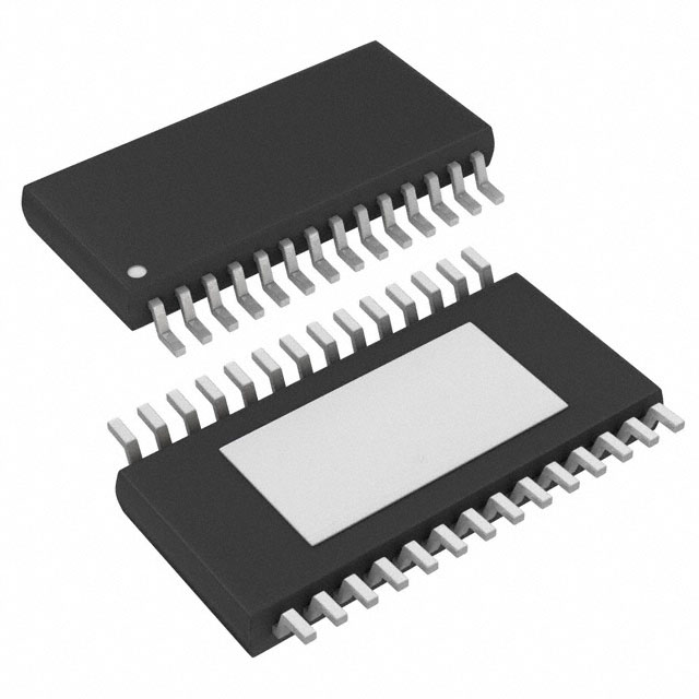
Datasheet
Driver IC for PPC
High Performance, High Reliability
36V 2ch DC Brush Motor Drivers
for PPC's etc.
BD62210AEFV
General Description
BD62210AEFV is a built-in 2 channel H-bridge motor
driver for 2 DC brush motors or 1 stepper motor. This
driver can facilitate low power consumption by direct
PWM or PWM constant current control. There are built in
protection circuits in this IC. It is possible to output an
abnormal detection signal for Wired-OR that notifies each
protection circuit operation, which contributes to set high
reliability.
Key Specifications
Power Supply Voltage Range:
Rated Output Current:
Rated Output Current (Peak):
Operating Temperature Range:
Output ON-Resistance:
(Total of upper and lower resistors)
Package
8 to 28 [V]
1.0 [A]
1.5 [A]
-25 to +85 [°C]
1.90 [Ω] (Typ)
W(Typ) x D(Typ)x H(Max)
Features
Single Power Supply Input (rated voltage of 36V)
Rated Output Current (peak): 1.0A(1.5A)
Low ON-Resistance DMOS Output
Forward, Reverse, Brake, Open
Power Save Function
External PWM Control
PWM Constant Current Control (current limit function)
Built-in Spike Noise Cancel Function (external noise
filter is unnecessary)
Driver for 2 DC Brush Motor
Driver for 1 Stepper motor
FULL STEP, HALF STEP (driving stepper motor)
µSTEP Drive by External DAC (driving stepper motor)
Built-in logic input pull-down resistor
Cross-conduction Prevention Circuit
Output detection signal during abnormal states
(Wired-OR)
Thermal Shutdown Circuit (TSD)
Over-current Protection Circuit (OCP)
Under Voltage Lock out Circuit (UVLO)
Over Voltage Lock out Circuit (OVLO)
Ghost Supply Prevention (protects against malfunction
when power supply is disconnected)
Adjacent Pins Short Protection
Inverted Mounting Protection
Microminiature, ultra-thin and high heat-radiation
(exposed metal type) HTSSOP-B28 package
HTSSOP-B28
9.70mm x 6.40mm x 1.00mm
Figure 1
Typical Application Circuit
9 GND
IN1A 16
IN1B 17
IN2A 19
IN2B 20
15
VREF1 11
VREF2 12
CR
TEST2
TEST1
2
3
4
10
FAILA
7 VCC1
5
Application
Plain Paper Copier (PPC), Multi-function Printer, Laser
Printer, Inkjet Printer, Photo Printer, FAX, Mini Printer and
etc.
13 PS
OUT1A
OUT1B
RNF1
RNF1S
VCC2
OUT2A
24
22
27
18
26
14
25
1
OUT2B
RNF2
RNF2S
GND
Figure 2. Typical Application Circuit
○Product structure:silicon monolithic integrated circuit ○This product has no designed protection against radioactive rays.
www.rohm.com
TSZ02201-0P2P0B301470-1-2
© 2016 ROHM Co., Ltd. All rights reserved.
1/21
TSZ22111・14・001
21.Jun.2016 Rev.001
�BD62210AEFV
Pin Configuration
Block Diagram
[TOP VIEW]
GND
28
1
27
NC
OUT1B
2
RNF1
3
RNF1S
4
25
RNF2S
OUT1A
5
24
OUT2A
NC
6
23
NC
26
OUT2B
11
+
-
12
+
-
+
1/8
-
RNF1S
1/8
15
Regulator
+
-
RNF2S
RNF2
Blank time
PWM control
10
TSD
OCP
UVLO
OVLO
OSC
7
VCC2
16
NC
8
21
NC
GND
9
20
IN2B
CR 10
19
IN2A
17
19
20
VREF1 11
18
TEST2
13
VREF2 12
17
IN1B
18
Forward
Reverse
Brake
Open
Forward
Reverse
Brake
Open
2
3
Predriver
22
7
Control logic
VCC1
5
4
22
24
27
26
25
14
PS 13
16
IN1A
TEST1 14
15
FAILA
1,9
Figure 3. Pin Configuration
Figure 4. Block Diagram
Pin Descriptions
Pin No.
Pin Name
1
GND
2
OUT1B
3
RNF1
4
RNF1S
5
OUT1A
Function
Pin No.
Pin name
Function
Ground terminal
15
FAILA
Output signal to detect abnormal
states
H bridge output terminal
16
IN1A
H bridge control terminal
17
IN1B
H bridge control terminal
18
TEST2
19
IN2A
No connection
20
IN2B
Power supply terminal
21
NC
No connection
22
VCC2
Ground terminal
23
NC
Connection terminal of CR
for setting switching frequency
24
OUT2A
H bridge output terminal
Input terminal of current limit
comparator
Connection terminal of resistor
for output current detection
Input terminal of current limit
comparator
H bridge output terminal
6
NC
7
VCC1
8
NC
9
GND
10
CR
11
VREF1
Current limit value setting terminal
25
RNF2S
12
VREF2
Current limit value setting terminal
26
RNF2
13
PS
Power save terminal
27
OUT2B
14
TEST1
Test terminal
28
NC
www.rohm.com
© 2016 ROHM Co., Ltd. All rights reserved.
TSZ22111・15・001
(Connected to GND)
2/21
Test terminal (Connected to GND)
H bridge control terminal
H bridge control terminal
No connection
Power supply terminal
No connection
Connection terminal of resistor
for output current detection
H bridge output terminal
No connection
TSZ02201-0P2P0B301470-1-2
21.Jun.2016 Rev.001
�BD62210AEFV
Absolute Maximum Ratings (Ta=25°C)
Parameter
Symbol
Rating
VCC1,2
-0.2 to +36.0
Supply Voltage
Unit
V
1.45
(Note 1)
W
4.70
(Note 2)
W
Power Dissipation
Pd
Input Voltage for Control Pin
VIN
-0.2 to +5.5
V
VRNF
0.7
V
RNF Maximum Voltage
IOUT
1.0
(Note 3)
IOUTPEAK
1.5
(Note 4)
Output Current
Output Current (peak)
A/ch
A/ch
Operating Temperature Range
Topr
-25 to +85
°C
Storage Temperature Range
Tstg
-55 to +150
°C
(Note 1) 70mm×70mm×1.6mm glass epoxy board. Derate by11.6mW/°C when operating above Ta=25°C.
(Note 2) 4-layer recommended board. Derate by 37.6mW/°C when operating above Ta=25°C.
(Note 3) Do not, however exceed Pd, ASO and Tjmax=150°C.
(Note 4)Pulse width tw ≤1ms, duty 20ms
Caution: Operating the IC over the absolute maximum ratings may damage the IC. The damage can either be a short circuit between pins or an open circuit
between pins and the internal circuitry. Therefore, it is important to consider circuit protection measures, such as adding a fuse, in case the IC is operated
over the absolute maximum ratings.
Recommended Operating Conditions (Ta= -25 to +85°C)
Parameter
Supply Voltage
Maximum Output Current (Continuous)
Symbol
VCC1,2
IOUT
Range
8 to 28
0.7
(Note 5)
Unit
V
A/ch
(Note 5) Do not, however exceed Pd, ASO and Tjmax=150°C.
www.rohm.com
© 2016 ROHM Co., Ltd. All rights reserved.
TSZ22111・15・001
3/21
TSZ02201-0P2P0B301470-1-2
21.Jun.2016 Rev.001
�BD62210AEFV
Electrical Characteristics (Unless otherwise specified Ta=25°C, VCC1.2=24V)
Parameter
Symbol
Limit
Unit
Conditions
Min
Typ
Max
ICCST
-
-
10
µA
PS=L
ICC
-
2.5
5.0
mA
PS=H, VREFx=2V
H Level Input Voltage
VIN2H
2.0
-
-
V
L Level Input Voltage
VIN2L
-
-
0.8
V
H Level Input Current
IIN2H
35
50
100
µA
VIN2=5V
L Level Input Current
IIN2L
-10
0
-
µA
VIN2=0V
IOUT =±1.0A
(Sum of upper and lower)
【Whole】
Circuit Current at Standby
Circuit Current
【Control Input】
【Output (OUT1A, OUT1B, OUT2A, OUT2B)】
Output ON-Resistance
RON
-
1.90
2.50
Ω
Output Leak Current
ILEAK
-
-
10
µA
IRNF
-80
-40
-
µA
RNFx=0V
VREFx Input Current
IVREF
-2.0
-0.1
-
µA
VREFx=0V
VREFx Input Voltage Range
Minimum on Time
(Blank Time)
Current Limit
Comparator Threshold
VVREF
0
-
2.0
V
tONMIN
0.7
1.5
3.0
µs
VCTH
0.23
0.25
0.27
V
【Current Control】
RNFX Input Current
www.rohm.com
© 2016 ROHM Co., Ltd. All rights reserved.
TSZ22111・15・001
4/21
VREFx=2V
TSZ02201-0P2P0B301470-1-2
21.Jun.2016 Rev.001
�BD62210AEFV
Application Information
1. Points to Notice for Terminal Description and PCB Layout
(1) PS/ Power Save Terminal
PS can make circuit into standby state and make motor outputs OPEN.
Please be careful because there is a delay of 40μs (max) before it returns from OFF state to normal state.
PS
State
L
H
POWER SAVE (STANDBY)
ACTIVE
(2) IN1A,I N1B, IN2A, IN2B/ H Bridge Control Terminal
It decides output logic for H bridge.
Input
Output
IN1A
IN1B
OUT1A
OUT1B
PS
IN2A
IN2B
OUT2A
OUT2B
L
X
X
OPEN
OPEN
H
L
L
OPEN
OPEN
H
H
L
H
L
H
L
H
L
H
H
H
H
L
L
X: H or L
State
POWER SAVE (STANDBY)
STOP
FORWARD
REVERSE
BRAKE
(3) TEST1,TEST2/ Terminal for Testing
This is the terminal used at the time of distribution test. Please connect to GND. Please be careful because there is a
possibility of malfunction if it is not connected to GND.
(4) VCC1,VCC2/ Power Supply Terminal
Motor’s drive current is flowing in it, so please connect it in such a way that the wire is thick & short and has low
impedance. VCC voltage may have great fluctuation, so please connect the bypass capacitor (100uF to 470uF) as
close as possible to the terminal. Adjust in such a way that the VCC voltage is stable. Please increase the
capacitance if needed, especially when large current or motors that have great back electromotive force are used. In
addition, to reduce the power supply’s impedance in wide frequency bandwidth, parallel connection of multi-layered
ceramic capacitor (0.01µF to 0.1µF) is recommended. Extreme care must be observed to make sure that the VCC
voltage does not exceed the rating even for a moment. VCC1 & VCC2 are shorted inside IC, so please be sure to
short VCC1 & VCC2 externally when using. If used without shorting, malfunction or destruction may occur because of
concentration of current routes etc., so please make sure that they are shorted when in use. Moreover, there is a
built-in clamp component in the output terminal to prevent electrostatic destruction. If sudden pulse or surge voltage
of more than the maximum absolute rating is applied, the clamp component operates which can result to destruction.
Please be sure to not exceed the maximum absolute rating. It is effective to mount a Zener diode with maximum
absolute rating. Also, diode is inserted between VCC terminal and GND terminal to prevent electrostatic destruction.
If reverse voltage is applied between VCC terminal and GND terminal, there is a danger of IC destruction so please
be careful.
(5) GND/ Ground Terminal
In order to reduce the noise caused by switching current and to stabilize the internal reference voltage of IC, please
connect it in such a way that the wiring impedance from this terminal is made as low as possible to achieve the
lowest electrical potential no matter what operating state it may be.
(6) OUT1A,OUT1B,OUT2A,OUT2B/ H Bridge Output Terminal
Motor’s drive current is flowing in it, so please connect it in such a way that the wire is thick & short and has low
impedance. It is also effective to add a Schottky diode if output has great positive or negative fluctuation when large
current is applied. For example, a counter electromotive voltage etc. is great. Moreover, there is a built-in clamp
component in the output terminal to prevent electrostatic destruction. If sudden pulse or surge voltage of more than
the maximum absolute rating is applied, the clamp component operates which can result to destruction. Please be
sure to not exceed the maximum absolute rating.
(7) RNF1,RNF2/ Connection Terminal of Resistor for Detecting of Output Current
Please connect the resistor of 0.1Ω to 0.3Ω for current detection between this terminal and GND according to
application circuits (Figure 3,4) and consider the power consumption of the current-detecting resistor. Determine the
2
resistor in such a way that W=IOUT ・R[W] does not exceed the power dissipation of the resistor. In addition, please
connect it in such a way that it has low impedance and does not have impedance in common with other GND
patterns. This is because motor’s drive current flows in the pattern through RNF terminal to current-detecting resistor
to GND. Please do not exceed the rating because there is the possibility of circuits’ malfunction etc. if the RNF
voltage has exceeded the maximum rating (0.7V). Moreover, please be careful not to short RNF terminal to GND
because there is the danger that OCP or TSD will operate when large current flows without normal PWM constant
current control.. However, if RNF terminal is open, there is also the possibility of malfunction because output current
does not flow either. Please do not let it open.
www.rohm.com
© 2016 ROHM Co., Ltd. All rights reserved.
TSZ22111・15・001
5/21
TSZ02201-0P2P0B301470-1-2
21.Jun.2016 Rev.001
�BD62210AEFV
(8) RNF1S,RNF2S/ Input Terminal of Current Limit Comparator
In this series, RNFS terminal, which is the input terminal of current limit comparator, is independently arranged in
order to decrease the lowering of current-detection accuracy caused by the wire impedance inside the IC of RNF
terminal. Therefore, please make sure to connect RNF terminal and RNFS terminal together when using PWM
constant current control. In addition, in case of interconnection, the lowering of current-detection accuracy caused by
the impedance of board pattern between RNF terminal and the current-detecting resistor can be decreased because
the wires from RNFS terminal is connected near the current-detecting resistor. Moreover, please design the pattern in
such a way that there is no noise spike.
(9) VREF1,VREF2/ Output Current Value-setting Terminal
This is the terminal to set the output current value for PWM constant current control or motor locking.
The output current value can be set by VREF voltage and current-detecting resistor (RNF resistor).
Output current IOUT[A ] = {VREF[V ] / 8(division ratio inside IC )} / RNF [Ω]
Please avoid using it with VREF terminal open. If VREF terminal is open, there is possibility of malfunctions as the
setting current increases and a large current flows etc. This is caused by unstable input and increasing VREF voltage.
Please take note of the input voltage range because if voltage of over 2V is applied on VREF terminal, there is also a
danger that large current flows in the output and OCP or TSD will operate. Also, when selecting the resistance value
please take into consideration the outflow current (max 2μA) produced by resistance division. The minimum current,
which can be controlled by VREF voltage, is determined by motor coil’s L & R values and minimum ON time. There is
a minimum ON time in PWM drive.
(10) CR/ Connection terminal of CR for Setting Switching Frequency
This is the terminal to set the switching frequency of the output. Please connect the external C (330pF to 680pF) and
R (10kΩ to 150kΩ) between this terminal and GND. Please refer to page 8.
Please connect the external components to GND in such a way that the interconnection does not have impedance in
common with other GND patterns. In addition, please create the pattern design in such a way to keep such sudden
pulses as square wave etc. away and that there is no noise spike. Please mount the two components of C and R if
PWM constant current control is being used. This is because normal PWM constant current control cannot be used if
CR terminal is open or it is biased externally. When not using PWM constant current control, connect this terminal to
GND.
(11) FAILA/ Fault Signal Output Terminal
FAILA outputs low signal when Over-Current Protection (OCP) or Thermal Shutdown (TSD) operates.
Even if Under Voltage Lock Out (UVLO) or Over Voltage Lock Out (OVLO) operates, FAILA signal doesn’t turn low
(i.e. high).
This terminal is an open drain type, so please set the pull up resistor (5kΩ to 100kΩ) to power supply less than 7V
(i.e. 5V or 3.3V). If not using this terminal, please connect it to GND.
OCP
TSD
FAILA
OFF
OFF
ON
ON
OFF
ON
OFF
ON
H (OFF)
M (ON)
L (ON)
L (ON)
(12) NC Terminal
This terminal is unconnected electrically with IC internal circuit.
(13) IC Back Metal
For HTSSOP-B28 package, the metal heat sink is mounted on IC’s back side. It becomes a prerequisite to use this
metal as heat sink so please secure the heat sink area sufficiently by soldering it to the GND plane on the board. Get
as wide GND pattern as possible. Please be careful because the allowable power dissipation as shown in page 14
cannot be attained if the metal heat sink is not connected by solder. Moreover, the back side metal is shorted with IC
chip’s back side and it becomes the GND potential, so there is adanger of malfunction and destruction if it is shorted
with potentials other than GND. Therefore; please do not design patterns other than GND through the IC’s back side.
www.rohm.com
© 2016 ROHM Co., Ltd. All rights reserved.
TSZ22111・15・001
6/21
TSZ02201-0P2P0B301470-1-2
21.Jun.2016 Rev.001
�BD62210AEFV
Protection Circuits
(14) Thermal Shutdown (TSD)
This IC has a built-in Thermal Shutdown circuit for thermal protection. When the IC’s chip temperature rises above
175°C (Typ), the motor output becomes OPEN. Also, when the temperature returns to under 150°C (Typ), it
automatically returns to normal operation. However, even when TSD is in operation, if heat is continued to be applied
externally, heat overdrive can lead to destruction.
(15) Over-Current Protection (OCP)
This IC has a built in Over-Current Protection circuit as a provision against destruction when the motor outputs are
shorted to each other or VCC-motor output or motor output-GND is shorted. This circuit latches the motor output to
OPEN condition when the regulated threshold current flows for 4μs (typ). It returns with power reactivation or a reset
of the PS terminal. The over-current protection circuit aims to prevent the destruction of the IC only from abnormal
situations such as when motor output is shorted and it is not meant to be used as protection or security for the device.
Therefore, the device should not be designed to make use of the function of this circuit. After OCP operation, if
abnormal situations continues and returned by power reactivation or reset of the PS terminal happens repeatedly,
then OCP operates constantly. The IC may generate heat or otherwise deteriorate. When the L value of the wiring is
great due to the long wiring and the over-current flows, the output terminal voltage increases and the absolute
maximum values may be exceeded. As a result, there is a possibility of destruction. Also, when a current flows, which
is over the output current rating and under the OCP detection current, the IC can heat up to over Tjmax=150°C. This
can deteriorate the IC. Therefore, current which exceeds the output rating should not be applied.
(16) Under Voltage Lock Out (UVLO)
This IC has a built-in Under Voltage Lock Out function to prevent false operation such as IC output during power
supply under voltage. When the applied voltage to the VCC terminal goes under 5V (Typ), the motor output is set to
OPEN. This switching voltage has a 1V (Typ) hysteresis to prevent false operation by noise etc. Please be aware that
this protection circuit does not operate during power save mode.
(17) Over Voltage Lock Out (OVLO)
This IC has a built-in Over Voltage Lock Out function to protect the IC output and the motor during power supply over
voltage. When the applied voltage to the VCC terminal goes over 32V (Typ), the motor output is set to OPEN. This
switching voltage has a 1V (Typ) hysteresis and a 4μs (Typ) mask time to prevent false operation by noise etc.
Although this over voltage locked out circuit is built-in, there is a possibility of destruction if the absolute maximum
value for power supply voltage is exceeded. Therefore, the absolute maximum value should not be exceeded. Please
be aware that this protection circuit does not operate during power save mode.
(18) Ghost Supply Prevention (protects against malfunction when power supply is disconnected)
If a control signal (IN1A, IN1B, IN2A, IN2B, PS, VREF1, VREF2) is applied when there is no power supplied to the IC,
there is a function which prevents false operation by voltage applied via the electrostatic destruction prevention diode
from the control input terminal to the VCC, to this IC or to another IC’s power supply. Therefore, there is no
malfunction in the circuit even when voltage is supplied to these input terminals while there is no power supply.
www.rohm.com
© 2016 ROHM Co., Ltd. All rights reserved.
TSZ22111・15・001
7/21
TSZ02201-0P2P0B301470-1-2
21.Jun.2016 Rev.001
�BD62210AEFV
2. External PWM Control
This series can drive motors by IN1A, IN1B, IN2A, and IN2B input directly from the microcomputer (up to100kHz).
Decay mode can be SLOW DECAY or FAST DECAY.
SLOW DECAY (forward rotation)
PS
H
H
H
H
H
Input
IN1A
IN2A
H
H
H
H
H
Output
OUT1A
OUT1B
OUT2A
OUT2B
H
L
L
L
H
L
L
L
H
L
IN1B
IN2B
L
H
L
H
L
FAST DECAY (synchronous rectification, forward rotation)
Input
Output
IN1B
OUT1A
OUT1B
IN1A
PS
IN2A
IN2B
OUT2A
OUT2B
H
H
L
H
L
H
L
H
L
H
H
H
L
H
L
H
L
H
L
H
H
H
L
H
L
ON
SLOW DECAY
ON
SLOW DECAY
ON
State
ON
FAST DECAY
ON
FAST DECAY
ON
FAST DECAY
SLOW DECAY
OFF to OFF
ON to OFF
State
OFF to ON
ON to OFF
M
M
ON to ON
OFF to ON
ON to OFF
OFF to ON
Output ON
Current decay
Figure 5. Route of Regenerative Current during Current Decay
www.rohm.com
© 2016 ROHM Co., Ltd. All rights reserved.
TSZ22111・15・001
8/21
TSZ02201-0P2P0B301470-1-2
21.Jun.2016 Rev.001
�BD62210AEFV
3. PWM Constant Current Control
This function can limit the peak current or switching current in driving DC brush motor.
In addition, it can drive bipolar stepper motor by PWM constant current control.
(1) Current Control Operation
When the output transistor is turned on, the output current increases which raises the voltage over the current sense
resistor. When the voltage on the RNF pin reaches the voltage value set by the VREF input voltage, the current limit
comparator operates and enters current decay mode. The output is then held OFF for a period of time determined by
the RC time constant connected to the CR pin. The process repeats itself constantly for PWM operation.
(2) Blank Time (Fixed in Internal Circuit)
In order to avoid misdetection of output current due to RNF spikes that may occur when the output turns ON, the IC
employs an automatic current detection-masking period (tONMIN 1.5µs typ). During this period, the current detection is
disabled immediately after the output transistor is turned on. This allows for constant-current drive without the need
for an external filter.
(3) CR Timer
The CR component connected to the CR pin is repeatedly charged and discharged between the VCRH and VCRL
levels. The CR continues to discharge during this period until it reaches VCRL, at which point the IC output is
switched back ON.
The CR charge time (tcharge) and discharge time (tdischarge) are set by external components, according to the following
formulas. The total of tcharge and tdischarge yield the switching period, tswitch.
t ch arg e [s] = C ⋅ R'⋅ R / (R'+R ) ⋅ In [(VCR − 0.4 ) / (VCR − 1.0 )]
0.35
0.30
0.25
where:
V is the internal regulator voltage 5V(typ)
R' is the CR internal impedance 5kΩ(typ)
t disch arg e [s] = C ⋅ R ⋅ ⋅In [(1 + a ) / 0.4]
α [V]
VCR = V ⋅ R / (R'+R )
0.20
0.15
0.10
0.05
0.00
200
α: See the right graph
400
600
800
C [pF]
t CHOP [s] = t ch arg e + t disch arg e
Setting range: C (330pF to 680pF), R (10kΩ to 150kΩ)
Spike noise
Output current
Current limit value
0mA
RNF voltage
Current limit value
GND
VCRH(1.0+α typ)
CR voltage
VCRL(0.4V typ)
GND
Switching period tswitch
Figure 6. Timing Chart of CR Voltage, RNF Voltage and Output Current
www.rohm.com
© 2016 ROHM Co., Ltd. All rights reserved.
TSZ22111・15・001
9/21
TSZ02201-0P2P0B301470-1-2
21.Jun.2016 Rev.001
�BD62210AEFV
4. Control Sequence of Stepper Motor
The following sequence can control the stepper motor by FULL STEP or HALF STEP mode.
Example of control sequence and torque vector
FULL STEP
①
②
③
④
OUT1A
100%
IN1A
IN1B
4
1
IN2A
OUT2A
OUT2B
IN2B
100%
-100%
100%
IOUT(CH1)
IOUT(CH2)
3
-100%
IN1A
2
OUT1B
IN1B
IN2A
IN2B
OUT1A
OUT1B
OUT2A
OUT2B
①
H
L
H
L
H
L
H
L
②
L
H
H
L
L
H
H
L
③
L
H
L
H
L
H
L
H
④
H
L
L
H
H
L
L
H
Figure 7. FULL STEP Control Sequence
HALF STEP
①
②
③
④
⑤
⑥
⑦
⑧
OUT1A
100%
IN1A
1
IN1B
8
2
IN2A
OUT2B
IN2B
7
100%
-100%
100%
IOUT(CH1)
IOUT(CH2)
3
OUT2A
4
6
5
-100%
OUT1B
IN1A
IN1B
IN2A
IN2B
OUT1A
OUT1B
OUT2A
OUT2B
①
H
L
L
L
H
L
OPEN
OPEN
②
H
L
H
L
H
L
H
L
③
L
L
H
L
OPEN
OPEN
H
L
④
L
H
H
L
L
H
H
L
⑤
L
H
L
L
L
H
OPEN
OPEN
⑥
L
H
L
H
L
H
L
H
⑦
L
L
L
H
OPEN
OPEN
L
H
⑧
H
L
L
H
H
L
L
H
Figure 8. HALF STEP Control Sequence
www.rohm.com
© 2016 ROHM Co., Ltd. All rights reserved.
TSZ22111・15・001
10/21
TSZ02201-0P2P0B301470-1-2
21.Jun.2016 Rev.001
�BD62210AEFV
5. µSTEP Drive for Stepper Motor
Output current of channel 1 and channel 2 can be determined by VREF1, VREF2. Output logic can be done by IN1A,
IN1B, IN2A, IN2B. Therefore, linear voltage input by external DAC to VREF1, VREF2 enables to drive stepper motor in
µSTEP mode.
IN1A
IN1B
IN2A
IN2B
VREF1
VREF2
OUT(ch1)
OUT(ch2)
Figure 9. µSTEP Control Sequence and Output Current
6. Power Dissipation
Please confirm that the IC’s chip temperature Tj is not over 150°C. Consider the IC’s power consumption (W), package
power (Pd) and ambient temperature (Ta). When Tj=150°C is exceeded, the functions as a semiconductor do not
operate and problems such as parasitic and leaks occur. Constant use under these conditions leads to deterioration and
eventually destruction of the IC. Tjmax=150°C must be strictly obeyed under all circumstances.
(1) Thermal Calculation
The IC’s consumed power can be estimated roughly with the power supply voltage (VCC), circuit current (ICC), output
ON-Resistance (RONH, RONL) and motor output current value (IOUT).
The calculation method during external PWM drive, SLOW DECAY, driving channel 1 only is shown here:
When using both channel 1 and channel 2, calculate for each H bridge.
Consumed power of the VCC [W ] = VCC [V ]⋅ ICC [A ] ・・・・・・・①
Consumed power of the output DMOS [W ] =
(RONH[W] + RONL[W]) ⋅ IOUT[A ]2 ⋅ on _ duty[%] / 100
During output ON
(2 ⋅ RONL[W]) ⋅ IOUT[A ]2 ⋅ (100 − on _ duty[%] / 100 )
・・・②
During current decay
However, on duty: PWM on duty [%]
Upper P-Channel DMOS
Model Number
ON-Resistance RONH[Ω] (Typ)
BD62210AEFV
1.25
Lower N-Channel DMOS
ON-Resistance RONL[Ω] (Typ)
0.65
Consumed total power of IC W_total [W] = ① + ②
Junction temperatur e Tj = Ta[°C] + θja[°C / W ] ⋅ W _ total[W ]
However, the thermal resistance value θja [°C/W] differs significantly depending on circuit board conditions. Refer to the
Power Dissipation curve on page 14. Also, we are taking measurements of thermal resistance value θja of the actual
boards used. Please feel free to contact our salesman. The calculated values above are only theoretical. For actual
thermal design, please perform sufficient thermal evaluation for the application board used, and create the thermal design
with enough margin to not exceed Tjmax=150°C. Although not normally used, if the IC is to be used under specific or
strict heat conditions, please consider attaching an external Schottky diode between the motor output terminal and GND
to decrease heat from the IC.
www.rohm.com
© 2016 ROHM Co., Ltd. All rights reserved.
TSZ22111・15・001
11/21
TSZ02201-0P2P0B301470-1-2
21.Jun.2016 Rev.001
�BD62210AEFV
(2) Temperature Monitoring
There is a way to directly measure the approximate chip temperature by using the TEST2 terminal. However,
temperature monitor using TEST2 terminal is only for evaluation and experimenting, and must not be used in actual
usage conditions. TEST2 terminal has a protection diode to prevent electrostatic discharge. The temperature may be
monitored using this protection diode.
(a) Measure the terminal voltage when a current of IDIODE=50μA flows from the TEST2 terminal to the GND, without
supplying VCC to the IC. This measurement is the VF voltage inside the diode.
(b) Measure the temperature characteristics of this terminal voltage. (VF has a linear negative temperature factor
against the temperature.) With the results of these temperature characteristics, chip temperature may be
calibrated from the TEST terminal voltage.
(c) Supply VCC, confirm the TEST2 terminal voltage while running the motor, and the chip temperature can be
approximated from the results of (b).
VCC
-Vf [mV]
Circuitry
TEST2
Circuitry
IDIODE
V
25
150
Chip temperature Tj [°C]
Figure 10. Model Diagram for Measuring Chip Temperature
www.rohm.com
© 2016 ROHM Co., Ltd. All rights reserved.
TSZ22111・15・001
12/21
TSZ02201-0P2P0B301470-1-2
21.Jun.2016 Rev.001
�BD62210AEFV
7. Application Circuit Diagram
(1) Constant Voltage Control or External PWM Control
VREF1 11
+
-
1/8
+
-
3.3V or 5.0V
15
Regulator
FAILA
When using the fault output function
⇒Pull up resistor 5kΩ to 100kΩ.
When not using the fault output
function
⇒Connect to GND.
Refer to page 5.
10kΩ
RNF1S
VREF2 12
+
-
1/8
+
-
RNF2S
Blank time
PWM control
CR 10
Control input terminal.
Input PWM signal (~100kHz) at
external PWM control.
Refer to page 4 for detail.
TSD
OCP
UVLO
OVLO
OSC
Bypass capacitor.
Setting range is
100µF to 470µF (electrolytic)
0.01µF to 0.1µF(multilayer ceramic
etc.)
Refer to page 4 for detail.
Be sure to short VCC1 & VCC2.
7 VCC1
5
IN1B 17
Power save terminal
Refer to page 4 for detail.
Forward
Reverse
Brake
Open
IN2A 19
IN2B 20
3
Predriver
IN1A 16
2
Control logic
Forward
Reverse
Brake
Open
TEST2
TEST1
22
24
27
26
PS 13
Terminal for testing
Connect to GND.
4
25
18
14
1,9
OUT1A
M
OUT1B
RNF1
100µF
0.1µF
RNF1S
VCC2
OUT2A
M
OUT2B
RNF2
RNF2S
GND
Figure 11. Block Diagram & Application Circuit Diagram
(a) Input/Output table
PS
L
H
H
H
H
Input
IN1A
IN2A
X
L
H
L
H
IN1B
IN2B
X
L
L
H
H
X: H or L
(b) Example of external PWM control sequence
SLOW DECAY (forward rotation)
Input
IN1A
IN1B
PS
IN2A
IN2B
H
H
L
H
H
H
H
H
L
H
H
H
H
H
L
Output
OUT1A
OUT1B
OUT2A
OUT2B
OPEN
OPEN
OPEN
OPEN
H
L
L
H
L
L
Output
OUT1A
OUT1B
OUT2A
OUT2B
H
L
L
L
H
L
L
L
H
L
State
POWER SAVE (STANDBY)
STOP
FORWARD
REVERSE
BRAKE
State
ON
SLOW DECAY
ON
SLOW DECAY
ON
FAST DECAY (forward rotation)
PS
H
H
H
H
H
Input
IN1A
IN2A
H
L
H
L
H
www.rohm.com
© 2016 ROHM Co., Ltd. All rights reserved.
TSZ22111・15・001
IN1B
IN2B
L
H
L
H
L
Output
OUT1A
OUT1B
OUT2A
OUT2B
H
L
L
H
H
L
L
H
H
L
13/21
State
ON
FAST DECAY
ON
FAST DECAY
ON
TSZ02201-0P2P0B301470-1-2
21.Jun.2016 Rev.001
�BD62210AEFV
(2) PWM Constant Current Control
Sets the current limit value.
Input range: 0V to 2V
Refer to page 5 for detail.
3.3V or 5.0V
3.3V or 5.0V
4.7kΩ
3.3V or 5.0V
VREF1
11
+
-
12
+
-
4.7kΩ
4.7kΩ
When using the fault output function
⇒Pull up resistor 5kΩ to 100kΩ.
When not using the fault output
function
⇒Connect to GND.
Refer to page 5.
1/8
15
Regulator
+
-
FAILA
10kΩ
RNF1S
VREF2
1.2kΩ
1/8
+
-
RNF2S
Blank time
PWM control
CR 10
TSD
OCP
UVLO
OVLO
OSC
Bypass capacitor.
Setting range is
100µF to 470µF(electrolytic)
0.01uF to 0.1µF(multilayer ceramic
etc.)
Refer to page 4 for detail.
Be sure to short VCC1 & VCC2.
470pF
82kΩ
7 VCC1
Sets the switching frequency.
Setting range is
C:330pF to 680pF
R:10kΩ to 150kΩ
Refer to page 5, 8 for detail.
5
Control logic input terminal.
Refer to page 4.
IN2A 19
IN2B 20
PS 13
TEST2
Power save terminal
Refer to page 4 for detail.
Forward
Reverse
Brake
Open
3
Predriver
IN1B 17
2
Control logic
IN1A 16
Forward
Reverse
Brake
Open
4
22
24
27
26
25
18
14
1,9
TEST1
OUT1A
M
OUT1B
RNF1
0.2Ω
100µF
0.1µF
RNF1S
VCC2
Current
detection
setting
resistor.
0.1Ω to 0.3Ω
Refer to page 4, 5 for detail.
OUT2A
M
OUT2B
RNF2
0.2Ω
RNF2S
Current
detection
setting
resistor
0.1Ω to 0.3Ω
Refer to page 4, 5 for detail.
GND
Figure 12. Application Circuit Diagram of
Constant Voltage Control or External PWM Control
Terminal for testing
Connect to GND.
(a) Input/Output table
PS
L
H
H
H
H
Input
IN1A
IN2A
X
L
H
L
H
IN1B
IN2B
X
L
L
H
H
Output
OUT1A
OUT1B
OUT2A
OUT2B
OPEN
OPEN
OPEN
OPEN
H
L
L
H
L
L
State
POWER SAVE (STANDBY)
STOP
FORWARD
REVERSE
BRAKE
X: H or L
www.rohm.com
© 2016 ROHM Co., Ltd. All rights reserved.
TSZ22111・15・001
14/21
TSZ02201-0P2P0B301470-1-2
21.Jun.2016 Rev.001
�BD62210AEFV
I/O Equivalent Circuits
VCC
Circuitry
VREF1
VREF2
10kΩ
Control
input
RNF1S
RNF2S
500Ω
5kΩ
100kΩ
VCC
VREG(internal regulator)
VCC
OUT1B
OUT2B
OUT1A
OUT2A
5kΩ
5kΩ
CR
10kΩ
RNF1, RNF2
Circuitry
5kΩ
FAILA
Figure 14. I/O Equivalent Circuits
www.rohm.com
© 2016 ROHM Co., Ltd. All rights reserved.
TSZ22111・15・001
15/21
TSZ02201-0P2P0B301470-1-2
21.Jun.2016 Rev.001
�BD62210AEFV
Operation Notes
1. Reverse Connection of Power Supply
Connecting the power supply in reverse polarity can damage the IC. Take precautions against reverse polarity when
connecting the power supply, such as mounting an external diode between the power supply and the IC’s power supply
terminals.
2. Power Supply Lines
Design the PCB layout pattern to provide low impedance supply lines. Separate the ground and supply lines of the digital
and analog blocks to prevent noise in the ground and supply lines of the digital block from affecting the analog block.
Furthermore, connect a capacitor to ground at all power supply pins. Consider the effect of temperature and aging on the
capacitance value when using electrolytic capacitors.
3. Ground Voltage
Ensure that no pins are at a voltage below that of the ground pin at any time, even during transient condition.
4. Ground Wiring Pattern
When using both small-signal and large-current ground traces, the two ground traces should be routed separately but
connected to a single ground at the reference point of the application board to avoid fluctuations in the small-signal
ground caused by large currents. Also ensure that the ground traces of external components do not cause variations on
the ground voltage. The ground lines must be as short and thick as possible to reduce line impedance.
5. Thermal Consideration
Should by any chance the power dissipation rating be exceeded, the rise in temperature of the chip may result in
deterioration of the properties of the chip. The absolute maximum rating of the Pd stated in this specification is when the
IC is mounted on a 70mm x 70mm x 1.6mm glass epoxy board. In case of exceeding this absolute maximum rating,
increase the board size and copper area to prevent exceeding the Pd rating.
6. Recommended Operating Conditions
These conditions represent a range within which the expected characteristics of the IC can be approximately obtained.
The electrical characteristics are guaranteed under the conditions of each parameter.
7. Inrush Current
When power is first supplied to the IC, it is possible that the internal logic may be unstable and inrush current may flow
instantaneously due to the internal powering sequence and delays, especially if the IC has more than one power supply.
Therefore, give special consideration to power coupling capacitance, power wiring, width of ground wiring, and routing of
connections.
8. Operation Under Strong Electromagnetic Field
Operating the IC in the presence of a strong electromagnetic field may cause the IC to malfunction.
9. Testing on Application Boards
When testing the IC on an application board, connecting a capacitor directly to a low-impedance output pin may subject
the IC to stress. Always discharge capacitors completely after each process or step. The IC’s power supply should
always be turned OFF completely before connecting or removing it from the test setup during the inspection process. To
prevent damage from static discharge, ground the IC during assembly and use similar precautions during transport and
storage.
10. Inter-pin Short and Mounting Errors
Ensure that the direction and position are correct when mounting the IC on the PCB. Incorrect mounting may result in
damaging the IC. Avoid nearby pins being shorted to each other especially to ground, power supply and output pin.
Inter-pin shorts could be due to many reasons such as metal particles, water droplets (in very humid environment) and
unintentional solder bridge deposited in between pins during assembly to name a few.
11. Unused Input Terminals
Input terminals of an IC are often connected to the gate of a MOS transistor. The gate has extremely high impedance
and extremely low capacitance. If left unconnected, the electric field from the outside can easily charge it. The small
charge acquired in this way is enough to produce a significant effect on the conduction through the transistor and cause
unexpected operation of the IC. So unless otherwise specified, unused input terminals should be connected to the power
supply or ground line.
www.rohm.com
© 2016 ROHM Co., Ltd. All rights reserved.
TSZ22111・15・001
16/21
TSZ02201-0P2P0B301470-1-2
21.Jun.2016 Rev.001
�BD62210AEFV
Operation Notes – continued
12. Regarding Input Pins of the IC
This monolithic IC contains P+ isolation and P substrate layers between adjacent elements in order to keep them isolated.
P-N junctions are formed at the intersection of the P layers with the N layers of other elements, creating a parasitic diode or
transistor. For example (refer to figure below):
When GND > Pin A and GND > Pin B, the P-N junction operates as a parasitic diode.
When GND > Pin B, the P-N junction operates as a parasitic transistor.
Parasitic diodes inevitably occur in the structure of the IC. The operation of parasitic diodes can result in mutual
interference among circuits, operational faults, or physical damage. Therefore, conditions that cause these diodes to
operate, such as applying a voltage lower than the GND voltage to an input pin (and thus to the P substrate) should be
avoided.
Figure 15. Example of Monolithic IC Structure
13. Area of Safe Operation (ASO)
Operate the IC such that the output voltage, output current, and power dissipation are all within the Area of Safe Operation
(ASO).
14. Thermal Shutdown Circuit(TSD)
This IC has a built-in thermal shutdown circuit that prevents heat damage to the IC. Normal operation should always be
within the IC’s power dissipation rating. If however the rating is exceeded for a continued period, the junction temperature
(Tj) will rise which will activate the TSD circuit that will turn OFF all output pins. When the Tj falls below the TSD threshold,
the circuits are automatically restored to normal operation.
Note that the TSD circuit operates in a situation that exceeds the absolute maximum ratings and therefore, under no
circumstances, should the TSD circuit be used in a set design or for any purpose other than protecting the IC from heat
damage.
15. Over-Current Protection Circuit (OCP)
This IC has a built-in over-current protection circuit that activates when the output is accidentally shorted. However, it is
strongly advised not to subject the IC to prolonged shorting of the output.
16. Operation Under Strong Electromagnetic Field (BD62210AEFV)
Operating the IC in the presence of a strong electromagnetic field may cause the IC to malfunction.
17. The Back Side of the IC Package (Define the side where product markings are printed as front) (BD62210AEFV)
There is an exposed central pad on the back side of the IC package. Please mount by footprint dimensions described in the
Jisso Information for WSOF5. Connect it to ground. If it is not connected to ground, there is a possibility that the device
malfunctions or a large current is generated.
18. TEST Terminal (BD62210AEFV)
Be sure to connect TEST pin to GND.
www.rohm.com
© 2016 ROHM Co., Ltd. All rights reserved.
TSZ22111・15・001
17/21
TSZ02201-0P2P0B301470-1-2
21.Jun.2016 Rev.001
�BD62210AEFV
Power Dissipation
HTSSOP-B28
HTSSOP-B28 has exposed metal on the back. It is possible to dissipate heat using the through holes in the back of board
as well as the surfaces with large areas of copper foil heat dissipation patterns which greatly increases power dissipation.
The back metal is shorted to the back side of the IC chip, being a GND potential, therefore there is a possibility for
malfunction if it is shorted with any potential other than GND. It should be avoided. Also, it is recommended that the back
metal is soldered onto the GND. Please note that it has been assumed that this product will be used in the condition
wherein this back metal has undergone heat dissipation treatment to increase heat dissipation efficiency.
5.0
Measurement machine:TH156 (Kuwano Electric)
Measurement condition:ROHM board
Board size:70mm*70mm*1.6mm
(With through holes on the board)
The exposed metal of the backside is connected to the board with
solder.
4.70W
4
Board①:1-layer board (Copper foil on the back 0mm)
Board②:2-layer board (Copper foil on the back 15mm*15mm)
Board③:2-layer board (Copper foil on the back 70mm*70mm)
Board④:4-layer board (Copper foil on the back 70mm*70mm)
4.0
Power Dissipation:Pd [W]
3.30W
3
3.0
2.0
1.0
Board①:θja=86.2°C/W
Board②:θja=67.6°C/W /W
Board③:θja=37.9°C/W
Board④:θja=26.6°C/W
1.85W
2
1.45W
1
0
25
50
75
85 100
125
150
Ambient Temperature : Ta [°C]
Figure 13. HTSSOP-B28 Power Dissipation
www.rohm.com
© 2016 ROHM Co., Ltd. All rights reserved.
TSZ22111・15・001
18/21
TSZ02201-0P2P0B301470-1-2
21.Jun.2016 Rev.001
�BD62210AEFV
Selecting a model name when ordering
B
D
6
2
2
1
ROHM Model
0
A
E
F
V
Package type
EFV
HTSSOP-B28
-
E2
:
Packing, Forming specification
E2: Reel-wound embossed taping
● Marking Diagram
HTSSOP-B28 (TOP VIEW)
Part Number Marking
BD62210AEF
LOT Number
1PIN MARK
www.rohm.com
© 2016 ROHM Co., Ltd. All rights reserved.
TSZ22111・15・001
19/21
TSZ02201-0P2P0B301470-1-2
21.Jun.2016 Rev.001
�BD62210AEFV
Physical Dimension, Tape and Reel Information
Package Name
www.rohm.com
© 2016 ROHM Co., Ltd. All rights reserved.
TSZ22111・15・001
HTSSOP-B28
20/21
TSZ02201-0P2P0B301470-1-2
21.Jun.2016 Rev.001
�BD62210AEFV
Revision History
Date
Revision
21.Jun.2016
001
Changes
New Release
www.rohm.com
© 2016 ROHM Co., Ltd. All rights reserved.
TSZ22111・15・001
21/21
TSZ02201-0P2P0B301470-1-2
21.Jun.2016 Rev.001
�Notice
Precaution on using ROHM Products
1.
Our Products are designed and manufactured for application in ordinary electronic equipments (such as AV equipment,
OA equipment, telecommunication equipment, home electronic appliances, amusement equipment, etc.). If you
(Note 1)
intend to use our Products in devices requiring extremely high reliability (such as medical equipment
, transport
equipment, traffic equipment, aircraft/spacecraft, nuclear power controllers, fuel controllers, car equipment including car
accessories, safety devices, etc.) and whose malfunction or failure may cause loss of human life, bodily injury or
serious damage to property (“Specific Applications”), please consult with the ROHM sales representative in advance.
Unless otherwise agreed in writing by ROHM in advance, ROHM shall not be in any way responsible or liable for any
damages, expenses or losses incurred by you or third parties arising from the use of any ROHM’s Products for Specific
Applications.
(Note1) Medical Equipment Classification of the Specific Applications
JAPAN
USA
EU
CHINA
CLASSⅢ
CLASSⅡb
CLASSⅢ
CLASSⅢ
CLASSⅣ
CLASSⅢ
2.
ROHM designs and manufactures its Products subject to strict quality control system. However, semiconductor
products can fail or malfunction at a certain rate. Please be sure to implement, at your own responsibilities, adequate
safety measures including but not limited to fail-safe design against the physical injury, damage to any property, which
a failure or malfunction of our Products may cause. The following are examples of safety measures:
[a] Installation of protection circuits or other protective devices to improve system safety
[b] Installation of redundant circuits to reduce the impact of single or multiple circuit failure
3.
Our Products are designed and manufactured for use under standard conditions and not under any special or
extraordinary environments or conditions, as exemplified below. Accordingly, ROHM shall not be in any way
responsible or liable for any damages, expenses or losses arising from the use of any ROHM’s Products under any
special or extraordinary environments or conditions. If you intend to use our Products under any special or
extraordinary environments or conditions (as exemplified below), your independent verification and confirmation of
product performance, reliability, etc, prior to use, must be necessary:
[a] Use of our Products in any types of liquid, including water, oils, chemicals, and organic solvents
[b] Use of our Products outdoors or in places where the Products are exposed to direct sunlight or dust
[c] Use of our Products in places where the Products are exposed to sea wind or corrosive gases, including Cl2,
H2S, NH3, SO2, and NO2
[d] Use of our Products in places where the Products are exposed to static electricity or electromagnetic waves
[e] Use of our Products in proximity to heat-producing components, plastic cords, or other flammable items
[f] Sealing or coating our Products with resin or other coating materials
[g] Use of our Products without cleaning residue of flux (even if you use no-clean type fluxes, cleaning residue of
flux is recommended); or Washing our Products by using water or water-soluble cleaning agents for cleaning
residue after soldering
[h] Use of the Products in places subject to dew condensation
4.
The Products are not subject to radiation-proof design.
5.
Please verify and confirm characteristics of the final or mounted products in using the Products.
6.
In particular, if a transient load (a large amount of load applied in a short period of time, such as pulse. is applied,
confirmation of performance characteristics after on-board mounting is strongly recommended. Avoid applying power
exceeding normal rated power; exceeding the power rating under steady-state loading condition may negatively affect
product performance and reliability.
7.
De-rate Power Dissipation depending on ambient temperature. When used in sealed area, confirm that it is the use in
the range that does not exceed the maximum junction temperature.
8.
Confirm that operation temperature is within the specified range described in the product specification.
9.
ROHM shall not be in any way responsible or liable for failure induced under deviant condition from what is defined in
this document.
Precaution for Mounting / Circuit board design
1.
When a highly active halogenous (chlorine, bromine, etc.) flux is used, the residue of flux may negatively affect product
performance and reliability.
2.
In principle, the reflow soldering method must be used on a surface-mount products, the flow soldering method must
be used on a through hole mount products. If the flow soldering method is preferred on a surface-mount products,
please consult with the ROHM representative in advance.
For details, please refer to ROHM Mounting specification
Notice-PGA-E
© 2015 ROHM Co., Ltd. All rights reserved.
Rev.003
�Precautions Regarding Application Examples and External Circuits
1.
If change is made to the constant of an external circuit, please allow a sufficient margin considering variations of the
characteristics of the Products and external components, including transient characteristics, as well as static
characteristics.
2.
You agree that application notes, reference designs, and associated data and information contained in this document
are presented only as guidance for Products use. Therefore, in case you use such information, you are solely
responsible for it and you must exercise your own independent verification and judgment in the use of such information
contained in this document. ROHM shall not be in any way responsible or liable for any damages, expenses or losses
incurred by you or third parties arising from the use of such information.
Precaution for Electrostatic
This Product is electrostatic sensitive product, which may be damaged due to electrostatic discharge. Please take proper
caution in your manufacturing process and storage so that voltage exceeding the Products maximum rating will not be
applied to Products. Please take special care under dry condition (e.g. Grounding of human body / equipment / solder iron,
isolation from charged objects, setting of Ionizer, friction prevention and temperature / humidity control).
Precaution for Storage / Transportation
1.
Product performance and soldered connections may deteriorate if the Products are stored in the places where:
[a] the Products are exposed to sea winds or corrosive gases, including Cl2, H2S, NH3, SO2, and NO2
[b] the temperature or humidity exceeds those recommended by ROHM
[c] the Products are exposed to direct sunshine or condensation
[d] the Products are exposed to high Electrostatic
2.
Even under ROHM recommended storage condition, solderability of products out of recommended storage time period
may be degraded. It is strongly recommended to confirm solderability before using Products of which storage time is
exceeding the recommended storage time period.
3.
Store / transport cartons in the correct direction, which is indicated on a carton with a symbol. Otherwise bent leads
may occur due to excessive stress applied when dropping of a carton.
4.
Use Products within the specified time after opening a humidity barrier bag. Baking is required before using Products of
which storage time is exceeding the recommended storage time period.
Precaution for Product Label
A two-dimensional barcode printed on ROHM Products label is for ROHM’s internal use only.
Precaution for Disposition
When disposing Products please dispose them properly using an authorized industry waste company.
Precaution for Foreign Exchange and Foreign Trade act
Since concerned goods might be fallen under listed items of export control prescribed by Foreign exchange and Foreign
trade act, please consult with ROHM in case of export.
Precaution Regarding Intellectual Property Rights
1.
All information and data including but not limited to application example contained in this document is for reference
only. ROHM does not warrant that foregoing information or data will not infringe any intellectual property rights or any
other rights of any third party regarding such information or data.
2.
ROHM shall not have any obligations where the claims, actions or demands arising from the combination of the
Products with other articles such as components, circuits, systems or external equipment (including software).
3.
No license, expressly or implied, is granted hereby under any intellectual property rights or other rights of ROHM or any
third parties with respect to the Products or the information contained in this document. Provided, however, that ROHM
will not assert its intellectual property rights or other rights against you or your customers to the extent necessary to
manufacture or sell products containing the Products, subject to the terms and conditions herein.
Other Precaution
1.
This document may not be reprinted or reproduced, in whole or in part, without prior written consent of ROHM.
2.
The Products may not be disassembled, converted, modified, reproduced or otherwise changed without prior written
consent of ROHM.
3.
In no event shall you use in any way whatsoever the Products and the related technical information contained in the
Products or this document for any military purposes, including but not limited to, the development of mass-destruction
weapons.
4.
The proper names of companies or products described in this document are trademarks or registered trademarks of
ROHM, its affiliated companies or third parties.
Notice-PGA-E
© 2015 ROHM Co., Ltd. All rights reserved.
Rev.003
�Datasheet
General Precaution
1. Before you use our Pro ducts, you are requested to care fully read this document and fully understand its contents.
ROHM shall n ot be in an y way responsible or liabl e for fa ilure, malfunction or acci dent arising from the use of a ny
ROHM’s Products against warning, caution or note contained in this document.
2. All information contained in this docume nt is current as of the issuing date and subj ect to change without any prior
notice. Before purchasing or using ROHM’s Products, please confirm the la test information with a ROHM sale s
representative.
3.
The information contained in this doc ument is provi ded on an “as is” basis and ROHM does not warrant that all
information contained in this document is accurate an d/or error-free. ROHM shall not be in an y way responsible or
liable for an y damages, expenses or losses incurred b y you or third parties resulting from inaccur acy or errors of or
concerning such information.
Notice – WE
© 2015 ROHM Co., Ltd. All rights reserved.
Rev.001
�


 工商网监
湘ICP备2023018690号
工商网监
湘ICP备2023018690号
