LED Drivers for LCD Backlights
White Backlight LED Driver
for Medium to Large LCD Panels
(Switching Regulator Type)
BD6590MUV
No.11040EBT14
●Description
BD6590MUV is white LED driver IC with PWM step-up DC/DC converter that can boost max 40V and current driver that can
drive max 30mA. The wide and precision brightness can be controlled by external PWM pulse.
BD6590MUV has very accurate current drivers, and it has few current errors between each strings.
So, it will be helpful to reduce brightness spots on the LCD.
Small package type is suited for saving space.
●Features
1) High efficiency PWM step-up DC/DC converter (fsw=1.25MHz)
2) High accuracy & good matching current drivers (MAX30mA/ch)
3) Integrated 50V power Nch MOSFET
4) Soft start
5) Drive up to 10 in series 6strings in parallel
6) Input voltage range (4.5V ~ 5.5V)
7) Rich safety functions
・Over-voltage protection
・Over current limit
・LED terminal open/short protect
・External SBD open detect / Output short protection
・UVLO
・Thermal shutdown
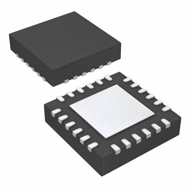
8) Small & thin package (VQFN024V4040) 4.0 × 4.0 × 1.0mm
●Applications
All middle size LCD equipments backlight of Notebook PC, NetPC,portable DVD player, DPF, etc.
●Absolute Maximum Ratings (Ta=25℃)
Parameter
Symbol
Ratings
Unit
Condition
Maximum applied voltage 1
VMAX1
7
V
Maximum applied voltage 2
VMAX2
25
V
VBAT, ISET, TEST, RSTB, PWMDRV
PWMPOW, VDET, FAILFLAG, OCPSET
LED1, LED2, LED3, LED4, LED5, LED6
Maximum applied voltage 3
SW
VMAX3
41
V
Power dissipation 1
Pd1
500
mW
*1
Power dissipation 2
Pd2
780
mW
*2
Power dissipation 3
Pd3
1510
mW
*3
Operating temperature range
Topr
-40 ~ +85
℃
-
Storage temperature range
Tstg
-55 ~ +150
℃
-
*1 Reduced 4.0mW/℃ With Ta>25℃ when not mounted on a heat radiation Board.
*2 1 layer (ROHM Standard board) has been mounted. Copper foil area 0mm2, When it’s used by more than Ta=25℃, it’s reduced by 6.2mW/℃.
*3 4 layer (JEDEC Compliant board) has been mounted. Copper foil area 1layer 6.28mm2, Copper foil area 2~4layers 5655.04mm2,
When it’s used by more than Ta=25℃, it’s reduced by 12.1mW/℃.
●Recommended Operating Range (Ta=-40℃ ~ +85℃)
Parameter
Symbol
Power supply voltage
www.rohm.com
© 2011 ROHM Co., Ltd. All rights reserved.
VBAT
Limits
Min.
Typ.
Max.
4.5
5.0
5.5
1/26
Unit
Condition
V
2011.07 - Rev.B
�BD6590MUV
Technical Note
●Electrical characteristic(Unless otherwise specified, VBAT=5V, Ta = +25℃)
Limits
Parameter
Symbol
Min.
Typ.
Max.
Unit
Condition
Quiescent current
Iq
-
0.1
4.4
µA
PWMPOW=PWMDRV=RSTB=0V
Current consumption
Idd
-
3.2
4.8
mA
VDET=0V,ISET=27kΩ
POWL
0
-
0.9
V
[PWMPOW Terminal]
Low input voltage range1
High input voltage range1
POWH
2.1
-
VBAT
V
Pull down resistor1
POWR
100
300
500
kΩ
PWMPOW=3V
[PWMDRV Terminal]
Low input voltage range2
PDRVL
0
-
0.9
V
High input voltage range2
PDRVH
2.1
-
5.5
V
DRVR
100
300
500
kΩ
FSL
0
-
0.9
V
Pull down resistor2
[FSEL Terminal]
Low input voltage range3
High input voltage range3
FSH
2.1
-
5.5
V
Pull down resistor3
FSR
100
300
500
kΩ
Input resistor
FFIR
1.0
2.0
3.0
kΩ
FAILFLAG=2.5V
Off current
FFIST
-
0.1
2.0
µA
PWMPOW=0V
UVLO
2.9
3.3
3.7
V
VBAT falling edge
LED control voltage
VLED
0.56
0.70
0.84
V
Switching frequency
fsw
1.00
1.25
1.50
MHz
Duty cycle limit
Duty
91
95.0
99.0
%
LED1-6=0.3V
SW Nch FET RON
RON
-
0.48
0.58
Ω
ISW=80mA
Over current limit
Ocp
1.4
2.0
2.6
A
OCPSET=68kΩ
OCPSET open protect
OOP
-
0.0
0.1
A
OCPSET=2MΩ
Over voltage limit Input
Ovl
0.96
1.00
1.04
V
Detect voltage of VDET pin
SBD open protect
Sop
0.02
0.05
0.08
V
Detect voltage of VDET pin
VDET leak current
OVIL
-
0.1
1.0
µA
LED maximum current
ILMAX
-
-
30
mA
LED current accuracy
ILACCU
-
-
±3.0
%
LED current matching
ILMAT
-
-
±1.5
%
LED current limiter
ILOCP
-
0
0.1
mA
LEDOVP
10.0
11.5
13.0
V
Iset
0.5
0.6
0.7
V
[FAILFLAG]
[Regulator]
Under voltage lock out
[Switching Regulator]
FSEL=L (GND short)
[Protection]
*1
[Current driver]
LED terminal over voltage protect
ISET voltage
ILED=16mA
Each LED current/Average (LED1-6)
ILED=16~20mA
Current limit value at ISET
resistor 1kΩ setting
PWMDRV=2.5V
*1 This parameter is tested with DC measurement.
www.rohm.com
© 2011 ROHM Co., Ltd. All rights reserved.
2/26
2011.07 - Rev.B
�BD6590MUV
Technical Note
●Block Diagram
VBAT
VBAT
FAILFLAG
SBD OPEN/
Output short PROTECT
VDET
UVLO
RSTB
Internal Power
Supply
Internal Reset
FAULT
DETECTOR
Internal Power
Control
PWMPOW
Output Over Voltage PROTECT
TSD
LED TERMINAL
OPEN/SHORT
DETECTOR
5.5V
Clamp
Soft start
ERRAMP
SW
PWM COMP
LED1
-
Control
SW
SENCE
LED2
LED3
LED
+
LED4
RETURN
LED5
SELECT
+
OSC
Current SENCE
LED6
Over Current Protect
8ch
PGND
+
-
ISET
Resistor driver
N.C. N.C. N.C.
OCPSET
TEST
GND
PWMDRV
Current Driver
ISET
GND
Fig.1 BD6590MUV block diagram
Adapter
●Application Example
Battery
4.5V to 30V
10µF
4.5V to 5.5V
10S × 6P
4.7µH
2.2µF/50V
1µF
FAILFLAG
SW
SW
VBAT
VBAT
1MΩ
10kΩ
PWMDRV
VDET
10KΩ
PWM
26.7kΩ
PWMPOW
fPWM=100Hz~1kHz
RESET
BD6590MUV
RSTB
LED1
TEST
LED2
LED3
LED4
LED5
LED6
OCPSET
68kΩ
Each 16mA
PGND
GND
GND
ISET
27kΩ
Fig.2 Application example (10LED × 6parallel)
www.rohm.com
© 2011 ROHM Co., Ltd. All rights reserved.
3/26
2011.07 - Rev.B
�BD6590MUV
Technical Note
●Pin Assignment Table
PIN No.
PIN Name
In/Out
1
2
3
4
5
6
7
8
9
10
11
12
13
14
5
16
17
18
19
20
21
22
23
24
SW
SW
N.C.
PGND
FAILFLAG
OCPSET
VDET
TEST
RSTB
ISET
GND
N.C.
LED1
LED2
LED3
LED4
LED5
LED6
N.C.
GND
PWMDRV
VBAT
PWMPOW
VBAT
Out
Out
Out
In
In
In
In
In
In
In
In
In
In
In
In
In
In
In
VBAT
Terminal
diagram
Function
Switching Tr drive terminal
Switching Tr drive terminal
No connect pin
PGND for switching Tr
Fail Flag
Current Limiter setting
Detect input for SBD open and OVP
TEST signal
Reset
Resister connection for LED current setting
GND for Switching Regulator
No connect pin
Current sink for LED
Current sink for LED
Current sink for LED
Current sink for LED
Current sink for LED
Current sink for LED
No connect pin
H
H
F
D
C
A
A
J
J
A
B
F
C
C
C
C
C
C
F
B
G
I
E
I
GND for Current driver
PWM input pin for power ON/OFF only driver
Regulator output / Internal power-supply
PWM input pin for power ON/OFF
Switching Tr drive terminal
VBAT
VBAT
PIN
PIN
PIN
GND
PIN
GND
PGND
A
GND
C
B
D
VBAT
VBAT
PIN
PIN
PIN
PIN
5.5V
Clump
GND
GND
E
F
PGND
G
H
VBAT
PIN
PIN
GND
PGND
I
www.rohm.com
© 2011 ROHM Co., Ltd. All rights reserved.
GND
J
4/26
2011.07 - Rev.B
�BD6590MUV
Technical Note
●Description of Functions
1) PWM current mode DC/DC converter
While BD6590MUV is power ON, the lowest voltage of LED terms is detected, PWM duty is decided to be 0.7V and output
voltage is kept invariably. As for the inputs of the PWM comparator as the feature of the PWM current mode, one is
overlapped with error components from the error amplifier, and the other is overlapped with a current sense signal that
controls the inductor current into Slope waveform to prevent sub harmonic oscillation. This output controls internal Nch Tr
via the RS latch. In the period where internal Nch Tr gate is ON, energy is accumulated in the external inductor, and in the
period where internal Nch Tr gate is OFF, energy is transferred to the output capacitor via external SBD.
BD6590MUV has many safety functions, and their detection signals stop switching operation at once.
2) Soft start
BD6590MUV has soft start function.
The soft start function prevents large coil current.
Rush current at turning on is prevented by the soft start function.
After PWMPOW, RSTB is changed L→ H, soft start becomes effective for within 4ms and soft start doesn't become
effective even if PWMPOW is changed L→H after that.
And, when the H section of PWMPOW is within 4ms, soft start becomes invalid when PWMPOW is input to H more than
three times. The invalid of the soft start can be canceled by making PWMPOW, PWMDRV →L.
PWMDRV
PWMPOW
PWMPOW
VREG
Max 1ms
Max 3ms
Soft start
VREG
Soft start
OFF
OFF
ON
OFF
Soft start
reset
OFF
ON
OFF
ON
OFF
OFF
OFF
OFF
Reset
Fig.3 Soft start
ON
Reset
Fig.4 Soft start reset and set
3) FAILFLAG
When the error condition occurs, boost operating is stopped by the protection function, and the error condition is outputted
from FAILFLAG. After power ON, when the protection function is operating under about 1ms have passed.
Object of protect function is as shown below.
・Over-voltage protection
・External SBD open detect/ Output Short protection
・LED terminal open/short protection
・Over current limit
PWMPOW
FAILFLAG
Protection
function
Boost
operating
about 1ms
un-detection
off
normal
detect
boost stop
un-detection
normal
off
normal
Fig.5 FAILFLAG operating description
www.rohm.com
© 2011 ROHM Co., Ltd. All rights reserved.
5/26
2011.07 - Rev.B
�BD6590MUV
Technical Note
●Protection
・Over voltage protection
At such an error of output open as the output DC/DC and the LED is not connected to IC, the DC/DC will boost too much
and the VDET terminal exceed the absolute maximum ratings, and may destruct the IC. Therefore, when VDET becomes
sensing voltage or higher, the over voltage limit works, and turns off the output Tr, and the pressure up made stop.
At this moment, the IC changes from activation into non-activation, and the output voltage goes down slowly. And, when
the Feedback of LED1 isn’t returned, so that Vout will return normal voltage.
Vout
LED1 voltage
LED1 connection normal
open
normal
LED2 connection
return
LED1 FeedBack
off
return
PWMPOW, PWMDRV
Fig.6 VDET operating description
・External SBD open detect / Output short protection
In the case of external SBD is not connected to IC, or VOUT is shorted to GND, the coil or internal Tr may be destructed.
Therefore, at such an error as VDET becoming 0.05V or below, and turns off the output Tr, and prevents the coil and the IC
from being destructed. And the IC changes from activation into non-activation, and current does not flow to the coil (0mA).
・Thermal shut down
BD6590MUV has thermal shut down function.
The thermal shut down works at 175℃ or higher, and the IC changes from activation into non-activation.
www.rohm.com
© 2011 ROHM Co., Ltd. All rights reserved.
6/26
2011.07 - Rev.B
�BD6590MUV
Technical Note
●How to set over voltage limit
This section is especially mentioned here because the spec shown electrical characteristic is necessary to explain this section.
Over voltage limit
min 0.96V typ 1.00V max 1.04V
LED control voltage
min 0.56V typ 0.70V max 0.84V
LED terminal over voltage protect min 10.0V typ 11.5 V max 13.0V
1. Calculate the conditions that the total value of LED VF is MAX.
Example) In the case of serial 8 LEDs with VF=2.9V(min), 3.2V(typ), 3.5V(max) => 3.5V x 8=28V
2.Then calculate the biggest value of output with the following formula.
The biggest value of output = the biggest value calculated for 1 + the biggest value of LED terminal voltage. (0.84V)
Example) The biggest value of output = 28V + 0.84V =28.84V
3.Set the smallest value of over voltage larger than the biggest value of output.
If over voltage is closer to the total value of VF, it could be occurred to detect over voltage by ripple, noise, and so on.
It is recommended that some margins should be left on the difference between over voltage and the total value of VF.
This time around 6% margin is placed.
Example) Against the biggest value of output = 28.84V, the smallest value of over voltage = 28.84V x 1.06 = 30.57V
Ic over voltage limit min=0.96V,typ=1.00V, max=1.04V
typ = 30.57V×(1.00V/0.96V) = 31.8V
max = 31.8V×(1.04V/1.00V) = 33.1V
4. The below shows how to control resistor setting over voltage
Please fix resistor high between VDET and output and then set over voltage after changing resistor between VDET and
GND. While PWM is off, output voltage decreases by minimizing this resistor. Due to the decrease of output voltage, ripple
of output voltage increases, and singing of output condenser also becomes bigger.
Example) Selecting OVP resistor.
(Example 1) VF=3.6V max, serial = 7 LED
OVP = 1.0V, R1 = 2.2MΩ, R2 = 78.7kΩ
VOUT = 1.0 × (2.2MΩ + 78.7kΩ)/ 78.7kΩ = 28.95V
VOUT
(Example 2) VF=3.6V max, serial = 8 LED
OVP = 1.0V, R1 = 2.2MΩ, R2 = 69.8kΩ
VOUT = 1.0 × (2.2MΩ + 69.8kΩ)/ 69.8kΩ = 32.52
(Example 3) VF=3.6V max, serial = 9 LED
OVP = 1.0V, R1 = 2.2MΩ, R2 = 62kΩ
VOUT = 1.0 × (2.2MΩ + 62kΩ)/ 62kΩ = 36.48V
(Example 4) VF=3.6V max, serial = 10 LED
OVP = 1.0V, R1 = 1.0MΩ, R2 = 26.7kΩ
VOUT = 1.0 × (1.0MΩ + 26.7kΩ)/ 26.7kΩ = 38.45V
R1
VDET
R2
Fig. 7 Control resistor setting
www.rohm.com
© 2011 ROHM Co., Ltd. All rights reserved.
7/26
2011.07 - Rev.B
�BD6590MUV
Technical Note
・Over Current Limit
Over current flows the current detection resistor that is connected to internal switching transistor source and between
PGND, Current sense voltage turns more than detection voltage decided with OCPSET, over current protection is
operating and it is prevented from flowing more than detection current by reducing ON duty of switching Tr without
stopping boost.As over current detector of BD6590MUV is detected peak current, current more than over current setting
value does not flow. And, over current value can decide freely by changing OCPSET voltage.
The range of over current setting is from 0.5A to 2.5A.
Current Sence
+
detect
-
R (OCPSET)=34kΩ×Over current setting
OCPSET
R(OCPSET)
Fig. 8 Architecture
TYP value of over current is 2A, MIN = 1.4A and MAX = 2.6A and after the
current value which was necessary for the normal operation was decided, detection resistor is derived by using MIN value
of over current detection value.
For example, detection resistor when typ value was set at 2A is given as shown below.
Detection resistor =34kΩ×2A=68kΩ
MAX current dispersion of this detection resistor value is
MAX current = 2A×1.3=2.6A
For example, 34kΩ → 1A, 68kΩ → 2A
As over current detector of BD6590MUV is detected the peak current, it have to estimate peak current to flow to the coil by
operating condition.
In case of, ○ Supply voltage of coil = VIN
○ Inductance value of coil = L
○ Switching frequency = fsw
MIN=1.0MHz, Typ=1.25MHz, MAX=1.5MHz
○ Output voltage = VOUT
○ Total LED current = IOUT
○ Average current of coil = Iave ○ Peak current of coil = Ipeak
○ Efficiency = eff
○ ON time of switching transistor = Ton
Ipeak = (VIN / L) × (1 / fsw) × (1-(VIN / VOUT))
Iave = (VOUT × IOUT / VIN) / eff
1/2
Ton = (Iave × (1-VIN/VOUT) × (1/fsw) × (L/VIN) × 2)
Each current is calculated.
As peak current varies according to whether there is the direct current superposed, the next is decided.
(1-VIN/VOUT) × (1/fsw) < Ton→
peak current = Ipeak /2 + Iave
(1-VIN/VOUT) × (1/fsw) > Ton→
peak current = = (VIN / L) ×Ton
(Example 1)
In case of, VIN=6.0V, L=4.7µH, fsw=1.25MHz, VOUT=39V, IOUT=80mA, Efficiency=85%
Ipeak = (6.0V / 4.7µH) × (1 / 1.25MHz) × (1-(6.0V / 39V)) =0.86A
Iave
= (39V × 80mA / 6.0V) / 85% = 0.61A
1/2
Ton
= (0.61A × (1-6.0V / 39V) × (1 / 1.25MHz) × (4.7µH /6.0V) × 2) = 0.81µs
(1-VIN/VOUT) × (1/fsw)=0.68µs < Ton
Peak current = 0.68A/2+0.61A = 1.04A
(Example 2)
In case of, VIN=12.0V, L=4.7µH, fsw=1.25MHz, VOUT=39V, IOUT=80mA, Efficiency=85%
Ipeak = (12.0V / 4.7µH) × (1 / 1.25MHz) × (1-(12V / 39V)) =1.41A
Iave = (39V × 80mA / 12.0V) / 85% = 0.31A
Ton
= (0.31A × (1-12 V / 39V) × (1 / 1.25MHz) × (4.7µH /12V) × 2)1/2 = 0.36µs
(1-VIN/VOUT) × (1/fsw)=0.55µs > Ton
Peak current = 12V/4.7µH × 0.36µs = 0.92A
*When too large current is set, output overshoot is caused, be careful enough because it is led to break down of
the IC in case of the worst.
www.rohm.com
© 2011 ROHM Co., Ltd. All rights reserved.
8/26
2011.07 - Rev.B
�BD6590MUV
Technical Note
・Soft start of over current limit for application
When the capacitor of OCPSET is set as figure, over current limit can become setting value slowly.
This effect is same as internal soft start.
When you want to reduce peak current than internal soft start on start up, this way is effective.
But, this action repeat when the timing that PWMPOW change L to H, so to do PWM control with PWMPOW terminal,rise
time of over current limit must be set into Hi time of PWM control, and please don’t connect the capacitor.
Show example of rising wave form with OCPSET 330pF.
PWMPOW
VOUT
OCPSET
36ms
Current Sence
1.5A
+
-
Zoom
Coil current
Detect
OCPSET
R(OCPSET)
Fig.9 VBAT=5V,
www.rohm.com
© 2011 ROHM Co., Ltd. All rights reserved.
6parallel 10serial 20mA/ch, OCPSET=68kΩ,330pF
9/26
2011.07 - Rev.B
�BD6590MUV
Technical Note
●Operating of the application deficiency
1) When 1 LED or 1string OPEN during the operating
The LED string that became OPEN isn't lighting, but other LED strings are lighting.
Then LED terminal is 0V, output boosts up to the over voltage protection voltage. When over voltage is detected,
the feedback of open string isn’t returned, so that VOUT will return normal voltage.
In the case that the voltage of 2 LED terminals becomes more than 25V(Absolute maximum ratings) as VOUT boosts up to
the over voltage protection voltage, please pay attention carefully that 2 LED terminals could be broken up in setting over
voltage protection.
OVP setting when selecting terminals
Vout
Over voltage protection voltage
40
LED1 voltage
35
LED2 voltage
30
LED 1 connection
25
20
LED1
LED2
Setting range of over voltage protection
15
normal
return
LED 1 feedback
10
open
normal
LED connection
off
return
PWMPOW, PWMDRV
5
LED 1current
0
10
20
30
LED Vf
(Vout)
40
20mA
LED 2 current
0mA
20mA
Fig.10 LED OPEN detect
Moreover, excessively high level of over voltage limit in terminal setting makes it happen that LED terminal voltage
exceeds LED terminal over voltage protect, which accordingly turn off LED lights. In order to prevent this problem, please
see “How to set the external resistor of over voltage limit (p.7)” and then set over voltage referring to application.
2) When LED short-circuited in the plural
All LED strings is turned on unless LED1~6 terminal voltage is more than 11.5V.
When it was more than 11.5V only the strings which short-circuited is turned off normally and LED current of other lines
continue to turn on.
LED terminal voltage
40
LED short
LED short-circuited
LED1 12.7V
35
30
0.7V
25
Vout
LED 1
LED 2
20
15
Voltage range of LED short-circuited
10
5
0
10
20
30
40
LED2
LED Vf
(Vout)
I LED1
20mA
I LED2
20mA
LED 1 FeedBack
normal
0mA
cut
Fig.11 LED short detect
3) When Schottky diode comes off
IC and a switching transistor aren't destroyed because boost operating stops by the Schottky diode coming off protected
function.
4) When the resistor of over current detection comes off
All the LEDs do not turn on due to open protect of the OCP resistor, which stops boost operation and consequently
prevents passing LED current.
www.rohm.com
© 2011 ROHM Co., Ltd. All rights reserved.
10/26
2011.07 - Rev.B
�BD6590MUV
Technical Note
●Control signal input timing
0V
4.1V
1
VBAT
VBAT
2
Min. 100µs
10kΩ
5V
PWMPOW
P IN
Rin
PWMDRV
GND
VREG
DC/DC VOUT
Fig.12 Control signal timing
Fig.13 Voltage with a control sign higher than VBAT
Example corresponding to application of conditions
In case you input control signs, such as PWMPOW, and PWMDRV, in the condition that the standup of supply voltage
(VBAT) is not completed, be careful of the following point.
①Input each control signal after VBAT exceeds 4.1V.
②When you input PWMPOW during the standup of VBAT, please give the standup time as Min.100µs
from 4.1V to stable voltage for VBAT.
There is no timing limitation at each input signal of PWMPOW and PWMDRV.
If each control sign changes into a condition higher than VBAT in (1) and (2), it goes via the ESD custody diode by the side of
VBAT of each terminal. A power supply is supplied to VBAT and there is a possibility of malfunctioning. In order to avoid this
condition, as shown in the above figure, please insert about 10kΩ in a signal line, and apply current qualification. Please
confirm an internal pull down resistor in the block diagram and electrical property.
●Start control (PWMPOW) and select LED current driver (PWMDRV)
BD6590MUV can control the IC system by PWMPOW, and IC can power off compulsory by setting 0.9V or below. Also,
It powers on PWMPOW is at more than 2.1V.
After it’s selected to PWMPOW=H, When it is selected at PWMDRV=H, LED current decided with ISET resistance flow.
Next, When it is selected at PWMDRV=L, LED current stop to flow.
RSTB
PWMPOW
PWMDRV
L
H, L
H, L
Off
OFF
H
L
L
Off
OFF
H
H
L
On
OFF
IC
LED current
H
L
H
Off
OFF
H
H
H
On
Current decided with ISET
●How to select the number of LED lines of the current driver
When the number of LED lines of the current driver is reduced, the un-select can be available by setting the unnecessary
LED1~6 terminals OPEN. In the case of using 4 lines and so on, please connect the unnecessary 2 lines OPEN.
Then please set RSTB,PWMPOW and PWMDRV “H” and finish selecting the lines within the process of softstart. If the level
of over voltage limit is set too high, the connected LED lines exceed LED terminal over voltage protect and are judged as
unnecessary lines.
Please make it sure referring “How to set over voltage limit (p.7)”.
Additionally, once the terminals are judged as unnecessary, this information never can be reset without setting RSTB,
PWMPOW and PWMDRV “L”.
www.rohm.com
© 2011 ROHM Co., Ltd. All rights reserved.
11/26
2011.07 - Rev.B
�BD6590MUV
Technical Note
●LED current setting range
LED current can set up Normal current by resistance value (RISET) connecting to ISET voltage.
Setting of each LED current is given as shown below.
Normal current = 432/RISET (A)
Also, Normal current setting range is 10mA~30mA. LED current becomes a leak current MAX 2µA at OFF setting.
When using beyond current setting range, please be careful that the error in LED current setting could be large.
ISET Normal current setting example
RISET
LED current
18kΩ (E24)
24.0mA
22kΩ (E24)
19.6mA
24kΩ (E24)
18.0mA
27kΩ (E24)
16.0mA
30kΩ (E24)
14.4mA
33kΩ (E24)
13.1mA
●Brightness control
There are two dimming method is available, first method is analog dimming that apply analog voltage to ISET terminal, and
second method is PWM control via digital dimming of PWMPOW or PWMDRV. Because each method has the different merit,
please choose a suitable method for the application of use.
Two techniques can be used as digital dimming by the PWM control One is PWM control of current driver, the other is PWM
control of power control.
As these two characteristics are shown in the below, selects to PWM control process comply with application.
・Efficiency emphasis in the low brightness which has an influence with the battery life
→ 2) Power control PWM control
・LED current dispersion emphasis in the PWM brightness control
→ 1) Current driver PWM control
(Reference)
Efficiency of LED current 0.5mA
PWM frequency 200Hz
PWM regulation process
(PWM Duty=2.5%)
Limit dispersion capability of low duty
Current driver
74.8%
0.04%
Power control
91%
0.40%
1) Current driver PWM control is controlled by providing PWM signal to PWMDRV, as it is shown Fig.14.
The current set up with ISET is chosen as the H section of PWMDRV and the current is off as the L section. Therefore, the
average LED current is increasing in proportion to duty cycle of PWMDRV signal. This method that it lets internal circuit
and DC/DC to work, because it becomes to switch the driver, the current tolerance is a few when the PWM brightness is
adjusted, so it makes it possible to brightness control until 5µs (MIN0.1% at 200Hz). And, don't use for the brightness
control, because effect of ISET changeover is big under 1µs ON time and under 1µs OFF time. Typical PWM frequency is
100Hz~25kHz.
PWMDRV
ON
OFF
LED current
ON
OFF
Coil current
ON
OFF
ON
IC’s active current
Fig.14 PWMDRV sequence
2) Power control PWM control is controlled by providing PWM signal to PWMPOW, as it is shown Fig.15. The current setting
set up with PWMDRV logic is chosen as the H section and the current is off as the L section. Therefore, the average LED
current is increasing in proportion to duty cycle of PWMPOW signal. This method is, because IC can be power-off at
off-time, the consumption current can be suppress, and the high efficiency can be available, so it makes it possible to
brightness control until 50µs (MIN1% at 200Hz). And, don't use for the brightness control, because effect of power
ON/OFF time changeover is big under 50µs ON time and under 50µs OFF time.
Typical PWM frequency is 100Hz~1kHz.
PWMPOW
ON
OFF
LED current
ON
OFF
Coil current
ON
OFF
ON
OFF
IC’s active current
Fig.15 PWMPOW sequence
www.rohm.com
© 2011 ROHM Co., Ltd. All rights reserved.
12/26
2011.07 - Rev.B
�BD6590MUV
Technical Note
●Output voltage ripple for PWM dimming
Conditions: 8serial 6parallel, LED current=20mA/ch, VBAT=5V, Coil Power=7V, Ta=25℃, output capacitor =2.2μF(50V/B3)
PWMDRV
Lower ripple Voltage
(under 200mV)
Output Voltage (AC)
780mA
Input Current
1ms/div.
●LED current rise and fall for PWM dimming
Conditions: 8serial 6parallel, LED current=20mA/ch, VBAT=5V, Coil Power=7V, Ta=25℃, output capacitor=2.2μF(50V/B3)
PWMDRV
PWMDRV
Output Voltage
Output Voltage
114ns
624ns
LED Current
400ns/div.
PWMDRV(ta 25, Frequency 200Hz, LED 10x6ch)
LED current vs Duty
100
PWMPOW (ta 25, Frequency 200Hz LED 10x6ch)
LED current vs Duty
100
10
10
LED current[mA]
L E D c urre nt[m A ]
40ns/div.
LED Current
1
0.1
12V
6V
26V
0.01
1
10
0.1
1
10
100
Duty[%]
PWM characteristics of current driver PWM
www.rohm.com
12V
6V
26V
0.001
100
duty[%]
© 2011 ROHM Co., Ltd. All rights reserved.
0.1
0.01
0.001
0.1
1
PWM characteristics of power control PWM
13/26
2011.07 - Rev.B
�BD6590MUV
Technical Note
●Main characteristics of efficiency
Conditions: 10serial 6parallel, LED current=20mA/ch, output capacitor=2.2μF(50V/B3)
100
95
Ta=-40°C
90
Efficiency [%]
85
Ta=85°C
80
Ta=25°C
75
70
65
60
55
50
5
10
15
20
25
30
Coil Power [V]
Efficiency vs duty (10serial x 6strings)
efficiency for PWMPOW Control
Coil Power=12V Ta=25℃
100.0%
90.0%
efficiency(%)
80.0%
Efficiency[%]
70.0%
60.0%
50.0%
40.0%
30.0%
20.0%
10.0%
100%
90%
80%
70%
60%
50%
40%
30%
20%
10%
0%
0
0.0%
0
10
20
30
40 50 60
PWM Duty[%]
70
80
PWM Duty(%)
Efficiency of current driver PWM
www.rohm.com
© 2011 ROHM Co., Ltd. All rights reserved.
10 20 30 40 50 60 70 80 90 100
90 100
Efficiency of power control PWM
14/26
2011.07 - Rev.B
�BD6590MUV
Technical Note
●The coil selection
The DC/DC is designed by more than 4.7µH. When L value sets to a lower value, it is possibility that the specific
sub-harmonic oscillation of current mode DC / DC will be happened. Please do not let L value to 3.3µH or below.
And, L value increases, the phase margin of DC / DC becomes to zero. Please enlarge the output capacitor value when you
increase L value.
Example)
4.7µH
=
output capacitor
2.2µF/50V
1pcs
6.8µH
=
output capacitor
2.2µF/50V
2pcs
10µH
=
output capacitor
2.2µF/50V
3pcs
This value is just examples, please made sure the final judgment is under an enough evaluation.
●The separation of the IC power supply and coil power supply
BD6590MUV can work in separating the power source in both IC power supply and coil power supply. With this application, it
can obtain that decrease of IC power consumption, and the applied voltage exceeds IC rating 7V.
That application is shown in below Fig.16. The higher voltage source is applied to the power source of coil that is connected
from 4.5V to 5.5V into IC VBAT, please follow the recommend design in Fig.16. It connects VBAT terminal and VREG
terminal together at IC outside.
When the coil power supply is applied, it is no any problem even though IC power supply is the state of 0V. Although IC
power supply is set to 0V, pull-down resistance is arranged for the power off which cuts off the leak route from coil power
supply in IC inside, the leak route is cut off. And, there is no power on-off sequence of coil power supply and IC power supply.
Adapter
Battery
4.5V to 30V
10µF
4.5V to 5.5V
10S × 6P
4.7µH
2.2µF/50V
1µF
FAILFLAG
SW
SW
VBAT
VBAT
1MΩ
10kΩ
PWMDRV
VDET
10KΩ
PWM
26.7kΩ
PWMPOW
fPWM=100Hz~1kHz
RESET
RSTB
BD6590MUV
LED1
TEST
LED2
LED3
LED4
LED5
LED6
OCPSET
Each 16mA
68kΩ
PGND
GND
GND
ISET
27kΩ
Fig.16 Application at the time of power supply isolation (6parallel)
www.rohm.com
© 2011 ROHM Co., Ltd. All rights reserved.
15/26
2011.07 - Rev.B
�BD6590MUV
Technical Note
●PCB Layout
In order to make the most of the performance of BD6590MUV, its PCB layout is very important. Characteristics such as
efficiency and ripple and the likes change greatly with layout patterns, which please note carefully.
Adapter
Battery
4.5V to 30V
4.5V to 5.5V
CVL1
10µF
10LED × 6parallel
4.7µH
CVB1
2.2µF/50V
CO1
1µF
RVT
FAILFLAG
SW
SW
VBAT
VBAT
1MΩ
10kΩ
PWMDRV
VDET
10KΩ
PWM
PWMPOW
fPWM=100Hz~1kHz
RESET
RSTB
RVD
26.7kΩ
BD6590MUV
LED1
TEST
LED2
LED3
LED4
LED5
ROC
LED6
OCPSET
each16mA
68kΩ
PGND
GND
GND
ISET
27kΩ
RISET
Fig. 17 Layout
Connect input capacitor CVL1 (10μF) as close as possible between coil L1 and PGND.
Put input bypath capacitor CVB1 (1μF) as close as possible between VBAT and PGND pin.
Connect schottky barrier diode SBD as close as possible between coil1and SW pin.
Connect output capacitor CO1 between cathode of SBD and PGND.
Make both PGND sides of CVL1 and CO1 as close as possible.
>
Connect LED current setting resistor RISET(27kΩ) as close as possible between ISET pin and GND.
There is possibility to oscillate when capacity is added to ISET terminal, so pay attention that capacity isn’t added.
Connect Over current limit setting resistor ROC(68kΩ) as close as possible between OCPSET pin and GND.
< Over current limit setting resistor RVT(1MΩ) & RVD(26.7kΩ)>
Put over current limit setting resistor RVT(1MΩ) & RVD(26.7kΩ) as close as possible VDET pin so as not to make the
wire longer, which
possibly causes the noise and also detects over voltage protection by mistake.
GND is analog ground, and PGND is power ground. PGND might cause a lot of noise due to the coil current of PGND.
Try to connect with analog ground, after smoothing with input capacitor CVL1 and output capacitor CO1.
PAD is used for improving the efficiency of IC heat radiation. Solder PAD to GND pin (analog ground).
Moreover, connect ground plane of board using via as shown in the patterns of next page.
The efficiency of heat radiation improves according to the area of ground plane.
When those pins are not connected directly near the chip, influence is give to the performance of BD6150, and may limit
the current drive performance. As for the wire to the inductor, make its resistance component small so as to reduce electric
power consumption and increase the entire efficiency.
The layout pattern in consideration of these is shown in the next page.
www.rohm.com
© 2011 ROHM Co., Ltd. All rights reserved.
16/26
2011.07 - Rev.B
�BD6590MUV
Technical Note
● Recommended PCB Layout
L1
4.7µH
SBD
60V
4R7
C_VB1
2.2µF/10V
76
C_VL1
10µF/25V
U1
BD6590MUV
D6150
CO1
2.2µF/50V
R_VD
26.7kΩ
R_OC
56kΩ
R_VT
1 MΩ
R_ISET
22kΩ
Top Layer
Mid layer 1
Mid layer 2
Bottom layer
Fig. 18 PCB Layout
www.rohm.com
© 2011 ROHM Co., Ltd. All rights reserved.
17/26
2011.07 - Rev.B
�BD6590MUV
Technical Note
●Selection of external parts
Recommended external parts are as shown below.
When to use other parts than these, select the following equivalent parts.
▪Coil
Value
Manufacturer
4.7μH
4.7μH
10μH
4.7μH
4.7μH
TDK
TDK
TDK
TOKO
TOKO
Product number
LTF5022T-4R7N2R0-LC
VLP6810T-4R7M1R6
VLP6810T-100M1R1
A915AY-4R7M
B1015AS-4R7M
Vertical
5.0
6.3
6.3
5.2
8.4
Size
Horizontal
5.2
6.8
6.8
5.2
8.3
Height
2.2
1.0
1.0
3.0
4.0
DC current
(mA)
2000
1600
1100
1870
3300
DCR
(Ω)
0.073
0.167
0.350
0.045
0.038
▪Capacitor
Value
Pressure
[ Supply voltage capacitor ]
2.2μF
10V
4.7μF
25V
4.7μF
25V
10μF
25V
10μF
10V
[ Output capacitor ]
1μF
50V
1μF
50V
2.2μF
50V
2.2μF
50V
0.33μF
50V
Manufacturer
Product number
Vertical
Size
Horizontal
Height
TC
Capa
Tolerance
MURATA
MURATA
MURATA
MURATA
MURATA
GRM188B31A225K
GRM319R61E475K
GRM21BR61E475K
GRM31CB31E106K
GRM219R61A106K
1.6
3.2
2.0
3.2
2.0
0.8
1.6
1.25
1.6
1.25
0.8±0.1
0.85±0.1
1.25±0.1
1.6±0.2
0.85±0.15
B
X5R
X5R
B
X5R
+/-10%
+/-10%
+/-10%
+/-10%
+/-10%
MURATA
MURATA
TDK
MURATA
MURATA
GRM31MB31H105K
GRM21BB31H105K
C3225JB1H225K
GRM31CB31H225K
GRM219B31H334K
3.2
2.0
3.2
3.2
2.0
1.6
1.25
2.5
1.6
1.25
1.15±0.1
1.25±0.1
2.0±0.2
1.6±0.2
0.85±0.1
B
B
B
B
B
+/-10%
+/-10%
+/-10%
+/-10%
+/-10%
▪Resistor
Value
Tolerance
Manufacturer
10kΩ
15kΩ
18kΩ
22kΩ
24kΩ
27kΩ
30kΩ
33kΩ
56kΩ
62kΩ
68kΩ
75kΩ
2.2MΩ
±0.5%
±0.5%
±0.5%
±0.5%
±0.5%
±0.5%
±0.5%
±0.5%
±0.5%
±0.5%
±0.5%
±0.5%
±0.5%
ROHM
ROHM
ROHM
ROHM
ROHM
ROHM
ROHM
ROHM
ROHM
ROHM
ROHM
ROHM
ROHM
Product number
MCR03PZPZD1002
MCR03PZPZD1502
MCR03PZPZD1802
MCR03PZPZD2202
MCR03PZPZD2402
MCR03PZPZD2702
MCR03PZPZD3002
MCR03PZPZD3302
MCR03PZPZD5602
MCR03PZPZD6202
MCR03PZPZD6802
MCR03PZPZD7502
MCR03PZPZD2204
Vertical
1.6
1.6
1.6
1.6
1.6
1.6
1.6
1.6
1.6
1.6
1.6
1.6
1.6
Size
Horizontal
0.8
0.8
0.8
0.8
0.8
0.8
0.8
0.8
0.8
0.8
0.8
0.8
0.8
Height
0.45
0.45
0.45
0.45
0.45
0.45
0.45
0.45
0.45
0.45
0.45
0.45
0.45
Vertical
3.5
Size
Horizontal
1.6
Height
0.8
▪SBD
Pressure
Manufacturer
60V
ROHM
Product number
RB160M-60
The coil is the part that is most influential to efficiency. Select the coil whose direct current resistor (DCR) and current inductance characteristic is excellent. BD6xxx is designed for the inductance value of 4.7µH. Don’t use the inductance value.
less than 3.3μH. Select a capacitor of ceramic type with excellent frequency and temperature characteristics.
Further, select Capacitor to be used with small direct current resistance.
●About heat loss
In heat design, operate the DC/DC converter in the following condition.
(The following temperature is a guarantee temperature, so consider the margin.)
1. Ambient temperature Ta must be less than 85℃.
2. The loss of IC must be less than dissipation Pd.
www.rohm.com
© 2011 ROHM Co., Ltd. All rights reserved.
18/26
2011.07 - Rev.B
�BD6590MUV
Technical Note
●Notes for use
(1) Absolute Maximum Ratings
An excess in the absolute maximum ratings, such as supply voltage, temperature range of operating conditions, etc., can
break down devices, thus making impossible to identify breaking mode such as a short circuit or an open circuit. If any
special mode exceeding the absolute maximum ratings is assumed, consideration should be given to take physical safety
measures including the use of fuses, etc.
(2) Operating conditions
These conditions represent a range within which characteristics can be provided approximately as expected. The
electrical characteristics are guaranteed under the conditions of each parameter.
(3) Reverse connection of power supply connector
The reverse connection of power supply connector can break down ICs. Take protective measures against the breakdown
due to the reverse connection, such as mounting an external diode between the power supply and the IC’s power supply
terminal.
(4) Power supply line
Design PCB pattern to provide low impedance for the wiring between the power supply and the GND lines. In this regard,
for the digital block power supply and the analog block power supply, even though these power supplies has the same
level of potential, separate the power supply pattern for the digital block from that for the analog block, thus suppressing
the diffraction of digital noises to the analog block power supply resulting from impedance common to the wiring patterns.
For the GND line, give consideration to design the patterns in a similar manner.
Furthermore, for all power supply terminals to ICs, mount a capacitor between the power supply and the GND terminal. At
the same time, in order to use an electrolytic capacitor, thoroughly check to be sure the characteristics of the capacitor to
be used present no problem including the occurrence of capacity dropout at a low temperature, thus determining the
constant.
(5) GND voltage
Make setting of the potential of the GND terminal so that it will be maintained at the minimum in any operating state.
Furthermore, check to be sure no terminals are at a potential lower than the GND voltage including an actual electric
transient.
(7) Short circuit between terminals and erroneous mounting
In order to mount ICs on a set PCB, pay thorough attention to the direction and offset of the ICs. Erroneous mounting can
break down the ICs. Furthermore, if a short circuit occurs due to foreign matters entering between terminals or between
the terminal and the power supply or the GND terminal, the ICs can break down.
(8) Operation in strong electromagnetic field
Be noted that using ICs in the strong electromagnetic field can malfunction them.
(9) Inspection with set PCB
On the inspection with the set PCB, if a capacitor is connected to a low-impedance IC terminal, the IC can suffer stress.
Therefore, be sure to discharge from the set PCB by each process. Furthermore, in order to mount or dismount the set
PCB to/from the jig for the inspection process, be sure to turn OFF the power supply and then mount the set PCB to the jig.
After the completion of the inspection, be sure to turn OFF the power supply and then dismount it from the jig. In addition,
for protection against static electricity, establish a ground for the assembly process and pay thorough attention to the
transportation and the storage of the set PCB.
(10) Input terminals
In terms of the construction of IC, parasitic elements are inevitably formed in relation to potential. The operation of the
parasitic element can cause interference with circuit operation, thus resulting in a malfunction and then breakdown of the
input terminal. Therefore, pay thorough attention not to handle the input terminals, such as to apply to the input terminals a
voltage lower than the GND respectively, so that any parasitic element will operate. Furthermore, do not apply a voltage to
the input terminals when no power supply voltage is applied to the IC. In addition, even if the power supply voltage is
applied, apply to the input terminals a voltage lower than the power supply voltage or within the guaranteed value of
electrical characteristics.
(11) Ground wiring pattern
If small-signal GND and large-current GND are provided, It will be recommended to separate the large-current GND
pattern from the small-signal GND pattern and establish a single ground at the reference point of the set PCB so that
resistance to the wiring pattern and voltage fluctuations due to a large current will cause no fluctuations in voltages of the
small-signal GND. Pay attention not to cause fluctuations in the GND wiring pattern of external parts as well.
(12) External capacitor
In order to use a ceramic capacitor as the external capacitor, determine the constant with consideration given to a
degradation in the nominal capacitance due to DC bias and changes in the capacitance due to temperature, etc.
(13) Thermal shutdown circuit (TSD)
When junction temperatures become 175℃ (typ) or higher, the thermal shutdown circuit operates and turns a switch OFF.
The thermal shutdown circuit, which is aimed at isolating the LSI from thermal runaway as much as possible, is not aimed
at the protection or guarantee of the LSI. Therefore, do not continuously use the LSI with this circuit operating or use the
LSI assuming its operation.
(14) Thermal design
Perform thermal design in which there are adequate margins by taking into account the permissible dissipation (Pd) in
actual states of use.
(15) Selection of coil
Select the low DCR inductors to decrease power loss for DC/DC converter.
www.rohm.com
© 2011 ROHM Co., Ltd. All rights reserved.
19/26
2011.07 - Rev.B
�BD6590MUV
Technical Note
●Application example
・LED current setting controlled ISETH resistor.
21.5kΩ : 20.1mA
27.0kΩ : 16.0mA
14.7kΩ : 29.59mA
・Brightness control
Please input PWM pulse from PWMPOW or PWMDRV terminal.
Please refer to function
15inch panel
Adapter
Battery
4.5V to 30V
10µF
4.5V to 5.5V
4.7µH
10S × 6P
2.2µF/50V
1µF
FAILFLAG
SW SW
VBAT VBAT
1MΩ
10kΩ
VDET
PWMDRV
10kΩ
PWM
26.7kΩ
PWMPOW
fPWM=100Hz~1kHz
BD6590MUV
10kΩ
RESET
RSTB
LED1
TEST
LED2
LED3
LED4
LED5
LED6
OCPSET
Each 16mA
68kΩ
PGND
GND
GND
ISET
27kΩ
Fig.19
10series ×6Parallel, LED current 16mA,
Switching frequency 1250kHz setting example
Power control PWM application
Adapter
Battery
4.5V to 30V
10µF
4.5V to 5.5V
4.7µH
10S × 6P
2.2µF/50V
1µF
fPWM=100Hz~25kHz
FAILFLAG
SW SW
VBAT VBAT
1MΩ
10kΩ
PWM
10kΩ
VDET
PWMDRV
10kΩ
RESET
26.7kΩ
PWMPOW
BD6590MUV
RSTB
LED1
TEST
LED2
LED3
LED4
LED5
LED6
OCPSET
68kΩ
Each 16mA
PGND
GND
GND
ISET
27kΩ
Fig.20
10series×6parallel, LED current16mA,
Switching frequency 1250kHz setting example
Current driver PWM application
www.rohm.com
© 2011 ROHM Co., Ltd. All rights reserved.
20/26
2011.07 - Rev.B
�BD6590MUV
Technical Note
13~14inch panel
Adapter
10µF
Adapter
Battery
4.5V to 26.6V
Battery
4.5V to 26.6V
4.5V to 5.5V
4.7µH
10µF
8S × 6P
4.5V to 5.5V
4.7µH
8S × 6P
2.2µF/50V
2.2µF/50V
1µF
1µF
FAILFLAG
SW SW
VBAT VBAT
FAILFLAG
2.2MΩ
PWM
VDET
PWMDRV
10kΩ
PWM
RESET
BD6590MUV
10kΩ
RSTB
69.8kΩ
PWMPOW
BD6590MUV
RSTB
LED1
LED1
TEST
TEST
LED2
LED2
LED3
LED3
LED4
LED4
LED5
LED5
LED6
OCPSET
PGND
GND
GND
52.2kΩ
ISET
each16mA
PGND
GND
GND
ISET
27kΩ
27kΩ
Fig.21
LED6
OCPSET
Each 16mA
56kΩ
2.2MΩ
10kΩ
VDET
PWMDRV
fPWM=100Hz~1kHz
fPWM=100Hz~1kHz
RESET
VBAT VBAT
10kΩ
69.8kΩ
PWMPOW
SW SW
10kΩ
10kΩ
8series×6parallel, LED current 16mA,
Switching frequency 1250kHz setting example
Power control PWM application
Fig.22
8series×6parallel, LED current 16mA,
Switching frequency 1250kHz setting example
Current driver PWM application
10~12inch panel
Adapter
Battery
4.5V to 23.9V
10µF
4.5V to 5.5V
4.7µH
7S × 6P
2.2µF/50V
1µF
FAILFLAG
SW SW
VBAT VBAT
2.2MΩ
10kΩ
VDET
PWMDRV
10kΩ
PWM
78.7kΩ
PWMPOW
fPWM=100Hz~1kHz
RESET
BD6590MUV
10kΩ
RSTB
LED1
TEST
LED2
LED3
LED4
LED5
LED6
OCPSET
47kΩ
LED7
PGND
GND
GND
ISET
27kΩ
Fig.23
Each 16mA
7series×6parallel, LED current016mA,
Switching frequency 1250kHz setting example
Power control PWM application
www.rohm.com
© 2011 ROHM Co., Ltd. All rights reserved.
21/26
2011.07 - Rev.B
�BD6590MUV
Technical Note
7inch panel
Adapter
10µF
Adapter
Battery
4.5V to 26.6V
Battery
4.5V to 21.2V
4.5V to 5.5V
4.7µH
10µF
8S × 3P
4.5V to 5.5V
4.7µH
6S × 4P
2.2µF/50V
2.2µF/50V
1µF
1µF
FAILFLAG
SW SW
VBAT VBAT
FAILFLAG
2.2MΩ
SW SW
VBAT VBAT
2.2MΩ
10kΩ
10kΩ
PWMDRV
PWMDRV
VDET
10kΩ
PWM
fPWM=100Hz~1kHz
PWM
RSTB
69.8kΩ
PWMPOW
fPWM=100Hz~1kHz
BD6590MUV
10kΩ
RESET
VDET
10kΩ
69.8kΩ
PWMPOW
BD6590MUV
10kΩ
RESET
RSTB
LED1
LED1
TEST
TEST
LED2
LED2
LED3
LED3
LED4
LED4
LED5
LED5
LED6
OCPSET
Each 16mA
68kΩ
PGND
GND
GND
68kΩ
ISET
8series×3parallel, LED current 16mA,
Switching frequency 1250kHz setting example
Power control PWM application
Adapter
GND
GND
ISET
Fig.25
6series×4parallel, LED current 16mA,
Switching frequency 1250kHz setting example
Power control PWM application
Battery
4.5V to 26.6V
10µF
Each 16mA
PGND
27kΩ
27kΩ
Fig.24
LED6
OCPSET
4.5V to 5.5V
4.7µH
8S × 3P
2.2µF/50V
1µF
FAILFLAG
SW SW
VBAT VBAT
2.2MΩ
10kΩ
PWMDRV
VDET
10kΩ
PWM
69.8kΩ
PWMPOW
fPWM=100Hz~1kHz
BD6590MUV
10kΩ
RESET
RSTB
LED1
TEST
LED2
LED3
LED4
LED5
LED6
OCPSET
56kΩ
Each 40.2mA
PGND
GND
GND
ISET
21.5kΩ
Fig.26
8series×3parallel, LED current 40.2mA,
Switching frequency 1250kHz setting example
Power control PWM application
www.rohm.com
© 2011 ROHM Co., Ltd. All rights reserved.
22/26
2011.07 - Rev.B
�BD6590MUV
Technical Note
5inch panel
Adapter
Adapter
Battery
4.5V to 26.6V
10µF
10µF
Battery
4.5V to 26.6V
4.5V to 5.5V
4.5V to 5.5V
8S × 2P
4.7µH
8S × 2P
4.7µH
2.2µF/50V
2.2µF/50V
1µF
1µF
FAILFLAG
FAILFLAG
SW
SW
VBAT
VBAT
PWMDRV
PWMDRV
10kΩ
RSTB
2.2MΩ
VDET
69.8kΩ
PWMPOW
fPWM=100Hz~1kHz
BD6590MUV
10kΩ
RESET
VBAT
VBAT
10kΩ
PWM
69.8kΩ
PWMPOW
fPWM=100Hz~1kHz
SW
10kΩ
VDET
10kΩ
PWM
SW
2.2MΩ
10kΩ
RESET
RSTB
BD6590MUV
LED1
LED1
TEST
TEST
LED2
LED2
LED3
LED3
LED4
LED4
LED5
LED5
GND
GND
Each 40.2mA
68kΩ
Each 16mA
33kΩ
PGND
LED6
OCPSET
LED6
OCPSET
PGND
GND
GND
ISET
ISET
21.5kΩ
27kΩ
Fig.27
8series×2parallel, LED current16mA,
Switching frequency1250kHz setting example
Power control PWM application
Adapter
8series×2parallel, LED current 40.2mA,
Switching frequency 1250kHz setting example
Power control PWM application
Battery
4.5V to 26.6V
10µF
Fig.28
4.5V to 5.5V
8S × 2P
4.7µH
2.2µF/50V
1µF
FAILFLAG
SW
SW
VBAT
VBAT
2.2MΩ
10kΩ
PWMDRV
VDET
10kΩ
PWM
69.8kΩ
PWMPOW
fPWM=100Hz~1kHz
10kΩ
RESET
RSTB
BD6590MUV
LED1
TEST
LED2
LED3
LED4
LED5
LED6
OCPSET
Each 88.8mA
68kΩ
PGND
GND
GND
ISET
27kΩ
Fig.29
8series×2parallel, LED current 88.8mA,
Switching frequency 1250kHz setting example
Power control PWM application
www.rohm.com
© 2011 ROHM Co., Ltd. All rights reserved.
23/26
2011.07 - Rev.B
�BD6590MUV
Technical Note
Adapter
10µF
Adapter
Battery
4.5V to 13V
Battery
4.5V to 13V
4.5V to 5.5V
4.7µH
10µF
3S × 5P
4.5V to 5.5V
4.7µH
3S × 6P
2.2µF/50V
2.2µF/50V
1µF
1µF
FAILFLAG
SW SW
VBAT VBAT
FAILFLAG
2.2MΩ
SW SW
VBAT VBAT
2.2MΩ
10kΩ
10kΩ
10kΩ
PWM
PWM
RSTB
187kΩ
PWMPOW
fPWM=100Hz~1kHz
BD6590MUV
10kΩ
BD6590MUV
10kΩ
RESET
10kΩ
187kΩ
PWMPOW
fPWM=100Hz~1kHz
VDET
PWMDRV
VDET
PWMDRV
RESET
RSTB
LED1
LED1
TEST
TEST
LED2
LED2
LED3
LED3
LED4
LED4
LED5
LED5
LED6
OCPSET
Each 16mA
33kΩ
PGND
GND
GND
LED6
OCPSET
Each 29.6mA
47kΩ
PGND
ISET
GND
GND
ISET
14.6kΩ
27kΩ
Fig.30
3series×5parallel, LED current 16mA,
Switching frequency 1250kHz setting example
Power control PWM application
Adapter
3series×6parallel, LED current 29.6mA,
Switching frequency 1250kHz setting example
Power control PWM application
Adapter
Battery
4.5V to 13V
10µF
Fig.31
Battery
4.5V to 30V
4.5V to 5.5V
4.7µH
10µF
3S × 6P
4.5V to 5.5V
4.7µH
10S × 1P
2.2µF/50V
2.2µF/50V
1µF
1µF
FAILFLAG
SW SW
VBAT VBAT
FAILFLAG
2.2MΩ
SW SW
VBAT VBAT
1MΩ
10kΩ
10kΩ
VDET
PWMDRV
10kΩ
PWM
PWM
RSTB
26.7kΩ
PWMPOW
fPWM=100Hz~1kHz
BD6590MUV
10kΩ
RESET
VDET
10kΩ
187kΩ
PWMPOW
fPWM=100Hz~1kHz
PWMDRV
BD6590MUV
10kΩ
RESET
RSTB
LED1
LED1
TEST
TEST
LED2
LED2
LED3
LED3
LED4
LED4
LED5
LED5
LED6
OCPSET
47kΩ
Each 177.6mA
PGND
GND
GND
68kΩ
ISET
3series×6parallel, LED current 177.6mA,
Switching frequency 1250kHz setting example
Power control PWM application
www.rohm.com
© 2011 ROHM Co., Ltd. All rights reserved.
Each 177.6mA
PGND
GND
GND
ISET
14.7kΩ
14.7kΩ
Fig.32
LED6
OCPSET
24/26
Fig.33
10series×1parallel, LED current177.6mA,
Switching frequency 1250kHz setting example
Power control PWM application
2011.07 - Rev.B
�BD6590MUV
Technical Note
●Application example of Analog dimming
Control LED current to charged D/A voltage.
Show application example and typ control.
Please decide final value after you evaluated application, characteristic.
Coil Power
Battery or adapter
4.5V to 30V
10µF
4.5V t o 5.5V
4.7µH
10L ED ×6p ar al l el
PWM
VBAT
VBAT
SW
SW
PWMDRV
PWMPOW
RESET
VDET
62k Ω
fPWM =100Hz~ 1kHz
1µF
2.2M Ω
FAILFLAG
2.2µF
/ 50V
RSTB
BD6590MUV
LED2
LED3
TEST
LED4
OCPSET
LED6
ISET
GND
GND
LED5
PGND
68kΩ
LED1
470k Ω
22k Ω
D/A
LEDcurrent =
432
470kΩ
+
432
DAC
122kΩ
ISETvoltage
typ LEDcurrent =
432
470kΩ
+
432
122kΩ
DAC
0.6V
Fig.34 BD6590MUV Analog style optical application
www.rohm.com
© 2011 ROHM Co., Ltd. All rights reserved.
25/26
2011.07 - Rev.B
�BD6590MUV
Technical Note
●Ordering part number
B
D
6
Part No.
5
9
0
Part No.
M
U
V
-
Package
MUV: VQFN024V4040
E
2
Packaging and forming specification
E2: Embossed tape and reel
VQFN024V4040
4.0±0.1
4.0±0.1
1.0MAX
2.4±0.1
0.4±0.1
7
12
19
18
0.5
The direction is the 1pin of product is at the upper left when you hold
( reel on the left hand and you pull out the tape on the right hand
)
6
24
0.75
E2
2.4±0.1
1
2500pcs
(0.22)
+0.03
0.02 -0.02
S
C0.2
Embossed carrier tape
Quantity
Direction
of feed
1PIN MARK
0.08 S
Tape
13
+0.05
0.25 -0.04
1pin
Reel
(Unit : mm)
www.rohm.com
© 2011 ROHM Co., Ltd. All rights reserved.
26/26
Direction of feed
∗ Order quantity needs to be multiple of the minimum quantity.
2011.07 - Rev.B
�Notice
Notes
No copying or reproduction of this document, in part or in whole, is permitted without the
consent of ROHM Co.,Ltd.
The content specified herein is subject to change for improvement without notice.
The content specified herein is for the purpose of introducing ROHM's products (hereinafter
"Products"). If you wish to use any such Product, please be sure to refer to the specifications,
which can be obtained from ROHM upon request.
Examples of application circuits, circuit constants and any other information contained herein
illustrate the standard usage and operations of the Products. The peripheral conditions must
be taken into account when designing circuits for mass production.
Great care was taken in ensuring the accuracy of the information specified in this document.
However, should you incur any damage arising from any inaccuracy or misprint of such
information, ROHM shall bear no responsibility for such damage.
The technical information specified herein is intended only to show the typical functions of and
examples of application circuits for the Products. ROHM does not grant you, explicitly or
implicitly, any license to use or exercise intellectual property or other rights held by ROHM and
other parties. ROHM shall bear no responsibility whatsoever for any dispute arising from the
use of such technical information.
The Products specified in this document are intended to be used with general-use electronic
equipment or devices (such as audio visual equipment, office-automation equipment, communication devices, electronic appliances and amusement devices).
The Products specified in this document are not designed to be radiation tolerant.
While ROHM always makes efforts to enhance the quality and reliability of its Products, a
Product may fail or malfunction for a variety of reasons.
Please be sure to implement in your equipment using the Products safety measures to guard
against the possibility of physical injury, fire or any other damage caused in the event of the
failure of any Product, such as derating, redundancy, fire control and fail-safe designs. ROHM
shall bear no responsibility whatsoever for your use of any Product outside of the prescribed
scope or not in accordance with the instruction manual.
The Products are not designed or manufactured to be used with any equipment, device or
system which requires an extremely high level of reliability the failure or malfunction of which
may result in a direct threat to human life or create a risk of human injury (such as a medical
instrument, transportation equipment, aerospace machinery, nuclear-reactor controller, fuelcontroller or other safety device). ROHM shall bear no responsibility in any way for use of any
of the Products for the above special purposes. If a Product is intended to be used for any
such special purpose, please contact a ROHM sales representative before purchasing.
If you intend to export or ship overseas any Product or technology specified herein that may
be controlled under the Foreign Exchange and the Foreign Trade Law, you will be required to
obtain a license or permit under the Law.
Thank you for your accessing to ROHM product informations.
More detail product informations and catalogs are available, please contact us.
ROHM Customer Support System
http://www.rohm.com/contact/
www.rohm.com
© 2011 ROHM Co., Ltd. All rights reserved.
R1120A
�


 工商网监
湘ICP备2023018690号
工商网监
湘ICP备2023018690号
