Switching Regulator Series
Isolated DC/DC Converter
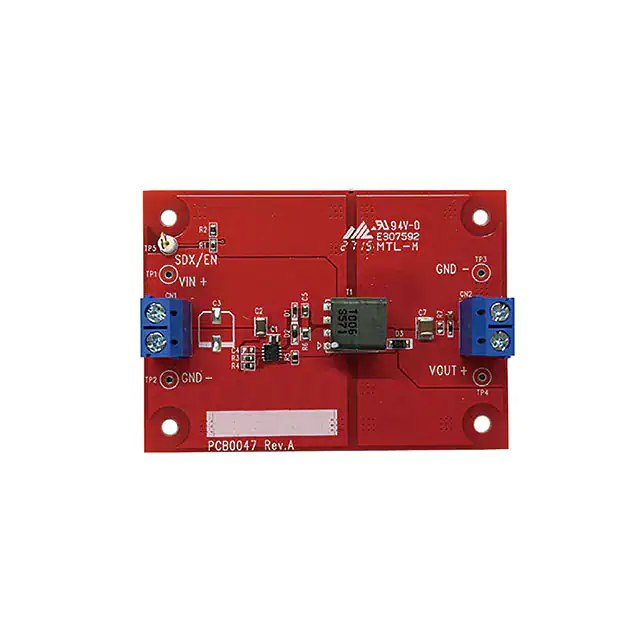
BD7F100HFN Evaluation Board
BD7F100HFN-EVK-001
General Description
BD7F100HFN-EVK-001 Evaluation Board outputs 5.0V voltage from 24V input using IC BD7F100HFN, an isolated DC/DC
converter. It supplies 800mA output current at maximum.
Performance specifications (The values listed here are representative values, which does not assure the characteristics.)
Unless otherwise is specified: VIN = 24V, VOUT = 5.0V
Parameter
Min
Typ
Max
Units
Input voltage range
24
V
Output voltage
5.0
V
Output current range
13.8
800
mA
Conditions
R4=3.9kΩ, R5=80.6kΩ
Maximum Output Power:4W
Input ripple voltage
80
mVpp
IO = 500mA
Output ripple voltage
80
mVpp
IO = 500mA
Output rise time
6
ms
Operating frequency
400
kHz
Maximum efficiency
76.7
%
www.rohm.co.jp
© 2016 ROHM Co., Ltd. All rights reserved.
1/11
IO = 800mA
2016.6.3 Rev.001
�BD7F100HFN-EVK-001
Operation Procedures
1. Required equipment
(1) DC power supply for 24V, 0.5A
(2) 800mA load at maximum
(3) DC voltmeter
2. Connect the equipment.
(1) Preset DC voltage to 24V and power supply output to OFF.
(2) Set load below 800mA to disable load.
(3) Connect the power supply positive terminal to VIN + terminal, and the negative terminal to GND - terminal, using a pair of
wires.
(4) Connect the load positive terminal to VOUT + terminal, and the negative terminal to GND - terminal, using a pair of wires.
(5) To measure input voltage, connect the DC voltmeter 1 positive terminal to TP1, and the negative terminal to TP2.
(6) To measure output voltage, connect the DC voltmeter 2 positive terminal to TP4, and the negative terminal to TP3.
(7) Turn ON DC voltage output.
(8) Check that the DC voltmeter 2 reads 5.0V.
(9) Enable load.
+
DC voltmeter 1
V
+
-
V
DC voltmeter 2
+
-
DC power
supply
Load
+
-
Figure 1. Connection Diagram
www.rohm.co.jp
© 2016 ROHM Co., Ltd. All rights reserved.
www.rohm.co.jp
2/11
2016.6.3 Rev.001
�BD7F100HFN-EVK-001
Setting Enable Voltage
As an IC operating condition, it is required to operate the converter with duty of 50% or less when the input
power supply is either ON or OFF.
If duty exceeds 50%, a phenomenon such as overshoot or overboosting happens. To avoid this, the condition
of following formula must be satisfied:
𝑉𝐷𝐼𝑆𝐴𝐵𝐿𝐸 >
𝑁𝑃
× (𝑉𝑂𝑈𝑇 + 𝑉𝐹 )
𝑁𝑆
VDISABLE: Stopping voltage
Np: Number of turns of transformer on the primary side
Ns: Number of turns of transformer on the secondary side
Vout: Output voltage
Vf: Forward voltage of output diode on the secondary side
To satisfy the input OFF voltage condition, put resistors R1 and R2 between the input and ground for the
division and connect SDX/EN terminal. This will enable start/stop with arbitrary input voltage.
The threshold at the time of SDX/EN terminal rise is set to 2.0V (Typ). At fall time, 0.2V (Typ) hysteresis
voltage is applied.
VENABLE
VDISABLE
VIN
2V
1.8V
SDX/EN
VOUT
Starting voltage can be set using the following formula:
𝑉𝐸𝑁𝐴𝐵𝐿𝐸 =
2.0𝑉 × (𝑅1 + 𝑅2)
𝑅2
Stopping voltage can be set using the following formula:
𝑉𝐷𝐼𝑆𝐴𝐵𝐿𝐸 =
1.8𝑉 × (𝑅1 + 𝑅2)
𝑅2
* Example
24V input: Connect R1=1MΩ and R2=120kΩ.
Starting voltage: 18.7V (Typ)
Stopping voltage: 16.9V (Typ)
www.rohm.co.jp
© 2016 ROHM Co., Ltd. All rights reserved.
www.rohm.co.jp
3/11
2016.6.3 Rev.001
�BD7F100HFN-EVK-001
Circuit Diagram
VIN = 24V, VOUT = 5.0V
SDX/EN
VIN(TP1)
D3
3,4
+
D1
C3
CN1
C2
C1
T1
7,8
VOUT+(TP4)
R1
C5
+
-
CN2
D4
R2
C7
2
3
AGND
VIN
SDX/EN
SW
COMP
REF
PGND
FB
D2
8
R3
-
R6
VOUT-(TP3)
7
6
R5
5
C8
9
4
U1 BD7F100HFN
FIN
1
R7
5,6
1,2
GND(TP2)
R4
C4
Figure 2. BD7F100HFN-EVK-001 Circuit Diagram
Parts List
No.
Value
Description
Size
Part Number / Series
Manufacture
C1
1μF
Capacitor, Chip, 50V, X7R
2012
GRM21BR71H105KA12
MURATA
C2
C3
C4
C5
C6
C7
C8
D1
4.7μF
1000pF
47μF
EDZV20B
Capacitor, Chip, 50V, X7R
Capacitor, Chip, 50V, CH
Capacitor, Chip, 10V, X7R
Diode, Zener
3216
1608
3225
1608
GRM31CR71H475KA12
GRM1882C1H102JA01
GRM32ER71A476KE15
EDZV20B
MURATA
MURATA
MURATA
ROHM
D2
RB160SS-40
Diode, Schottky
2512
RB160SS-40
ROHM
D3
RB160M-40
Diode, Schottky
3516
RB160M-40
ROHM
D4
VDZ6.2B
Diode, Zener
1406
VDZ6.2B
ROHM
R1
1MΩ
Resistor, Chip, 1/10W, 1%
1608
MCR03EZPF1004
ROHM
R2
R3
R4
R5
R6
R7
T1
120kΩ
0Ω
3.9kΩ
80.6kΩ
2kΩ
1kΩ
63μH
Resistor, Chip, 1/10W, 1%
Resistor, Chip, 1/10W, 1%
Resistor, Chip, 1/10W, 1%
Resistor, Chip, 1/10W, 1%
Resistor, Chip, 1/8W, 1%
Resistor, Chip, 1/10W, 1%
Transformer, Np:Ns=3:1, ±20%
1608
1608
1608
1608
2012
1608
10.0 x 10.0 x 11.5mm
MCR03EZPF1203
MCR03EZPJ000
MCR03EZPF3901
MCR03EZPF8062
MCR10EZHF2001
MCR03EZPF1001
CEP911B-2405051R
ROHM
ROHM
ROHM
ROHM
ROHM
ROHM
sumida
U1
BD7F100HFN
I.C. BD7F100HFN
HSON8
BD7F100HFN
ROHM
www.rohm.co.jp
© 2016 ROHM Co., Ltd. All rights reserved.
www.rohm.co.jp
4/11
2016.6.3 Rev.001
�BD7F100HFN-EVK-001
PCB Layout
Figure 3. Top Silk Screen (Top view)
Figure 4. Top Silk Screen and Layout
www.rohm.co.jp
© 2016 ROHM Co., Ltd. All rights reserved.
www.rohm.co.jp
5/11
(Top view)
2016.6.3 Rev.001
�BD7F100HFN-EVK-001
PCB Layout
Figure 5. Top Layout (Top view)
Figure 6. L2 Layout (Top view)
www.rohm.co.jp
© 2016 ROHM Co., Ltd. All rights reserved.
www.rohm.co.jp
6/11
2016.6.3 Rev.001
�BD7F100HFN-EVK-001
PCB Layout
Figure 7. L3 Layout (Top view)
Figure 8. Bottom Layout (Top view)
www.rohm.co.jp
© 2016 ROHM Co., Ltd. All rights reserved.
www.rohm.co.jp
7/11
2016.6.3 Rev.001
�BD7F100HFN-EVK-001
5.5
Limitation
with
SW
terminal
voltage
50V (Max)
Limitation with current limit 1A
(Min)
5.4
5.3
5.2
LOAD REG
5.1
5
4.9
4.8
4.7
4.6
4.5
0
0.2
0.4
0.6
0.8
OUT_CURRENT (A)
Figure 10. Load Regulation
Figure 9. Maximum Output Power
VIN = 24V
VOUT = 5.0V
VOUT (AC):100mV/div
IOUT: 500mA/div
IOUT: 300mA→800mA→300mA
Time scale 200us/div
Figure 11. Load Transient Characteristics
www.rohm.co.jp
© 2016 ROHM Co., Ltd. All rights reserved.
www.rohm.co.jp
8/11
2016.6.3 Rev.001
�BD7F100HFN-EVK-001
IOUT = 100mA
VIN (AC)
50mV/div
Time scale 2us/div
IOUT = 500mA
VIN (AC)
50mV/div
Time scale 2us/div
IOUT = 800mA
VIN (AC)
50mV/div
Figure 12. Input Voltage Ripple Waveform
VIN = 24V, VO = 5.0V
Time scale 2us/div
IOUT = 100mA
VOUT (AC)
50mV/div
Time scale 2us/div
IOUT = 500mA
VOUT (AC)
50mV/div
Time scale 2us/div
IOUT = 800mA
VOUT (AC)
50mV/div
Time scale 2us/div
Figure 13. Output Voltage Ripple Waveform
VIN = 24V, VOUT = 5.0V
www.rohm.co.jp
© 2016 ROHM Co., Ltd. All rights reserved.
www.rohm.co.jp
9/11
2016.6.3 Rev.001
�BD7F100HFN-EVK-001
EN
2V/div
VIN
10V/div
VOUT
2V/div
Time scale 50ms/div
Figure 14. Startup
VIN = 24V, VOUT = 5.0V, IOUT =100mA
Time scale 50ms/div
Figure 15. Power Down
VIN = 24V, VOUT = 5.0V, IOUT = 100mA
EN
2V/div
VIN
10V/div
VOUT
2V/div
Time scale 50ms/div
Figure 16. Startup
VIN = 24V, VOUT = 5.0V, IOUT =500mA
Time scale 50ms/div
Figure 17. Power Down
VIN = 24V, VOUT = 5.0V, IOUT = 500mA
EN
2V/div
VIN
10V/div
VOUT
2V/div
Time scale 50ms/div
Figure 18. Startup
VIN = 24V, VOUT = 5.0V, IOUT =800mA
www.rohm.co.jp
© 2016 ROHM Co., Ltd. All rights reserved.
www.rohm.co.jp
10/11
Time scale 50ms/div
Figure 19. Power Down
VIN = 24V, VOUT = 5.0V, IOUT = 800mA
2016.6.3 Rev.001
�BD7F100HFN-EVK-001
T1:41.8˚C
D1:55.2˚C
D3:49.1˚C
U1:42.6˚C
R6:62.5˚C
Figure 20. Parts Temperature
VIN = 24V, VO = 5.0V, IO =800mA
90
80
Efficiency (%)
70
60
50
40
30
20
10
0
0
0.2
0.4
0.6
0.8
OUT_CURRENT (A)
Figure 21. Efficiency
VIN = 24V, VO = 5.0V
www.rohm.co.jp
© 2016 ROHM Co., Ltd. All rights reserved.
www.rohm.co.jp
11/11
2016.6.3 Rev.001
�Notice
Notes
1) The information contained herein is subject to change without notice.
2) Before you use our Products, please contact our sales representative and verify the latest specifications :
3) Although ROHM is continuously working to improve product reliability and quality, semiconductors can break down and malfunction due to various factors.
Therefore, in order to prevent personal injury or fire arising from failure, please take safety
measures such as complying with the derating characteristics, implementing redundant and
fire prevention designs, and utilizing backups and fail-safe procedures. ROHM shall have no
responsibility for any damages arising out of the use of our Poducts beyond the rating specified by
ROHM.
4) Examples of application circuits, circuit constants and any other information contained herein are
provided only to illustrate the standard usage and operations of the Products. The peripheral
conditions must be taken into account when designing circuits for mass production.
5) The technical information specified herein is intended only to show the typical functions of and
examples of application circuits for the Products. ROHM does not grant you, explicitly or implicitly,
any license to use or exercise intellectual property or other rights held by ROHM or any other
parties. ROHM shall have no responsibility whatsoever for any dispute arising out of the use of
such technical information.
6) The Products are intended for use in general electronic equipment (i.e. AV/OA devices, communication, consumer systems, gaming/entertainment sets) as well as the applications indicated in
this document.
7) The Products specified in this document are not designed to be radiation tolerant.
8) For use of our Products in applications requiring a high degree of reliability (as exemplified
below), please contact and consult with a ROHM representative : transportation equipment (i.e.
cars, ships, trains), primary communication equipment, traffic lights, fire/crime prevention, safety
equipment, medical systems, servers, solar cells, and power transmission systems.
9) Do not use our Products in applications requiring extremely high reliability, such as aerospace
equipment, nuclear power control systems, and submarine repeaters.
10) ROHM shall have no responsibility for any damages or injury arising from non-compliance with
the recommended usage conditions and specifications contained herein.
11) ROHM has used reasonable care to ensur the accuracy of the information contained in this
document. However, ROHM does not warrants that such information is error-free, and ROHM
shall have no responsibility for any damages arising from any inaccuracy or misprint of such
information.
12) Please use the Products in accordance with any applicable environmental laws and regulations,
such as the RoHS Directive. For more details, including RoHS compatibility, please contact a
ROHM sales office. ROHM shall have no responsibility for any damages or losses resulting
non-compliance with any applicable laws or regulations.
13) When providing our Products and technologies contained in this document to other countries,
you must abide by the procedures and provisions stipulated in all applicable export laws and
regulations, including without limitation the US Export Administration Regulations and the Foreign
Exchange and Foreign Trade Act.
14) This document, in part or in whole, may not be reprinted or reproduced without prior consent of
ROHM.
Thank you for your accessing to ROHM product informations.
More detail product informations and catalogs are available, please contact us.
ROHM Customer Support System
http://www.rohm.com/contact/
www.rohm.com
© 2014 ROHM Co., Ltd. All rights reserved.
R1102A
�


 工商网监
湘ICP备2023018690号
工商网监
湘ICP备2023018690号

