Datasheet
BD9412F
General Description
Key Specifications
BD9412F is a current resonance type LED Driver with
frequency-controlled LED current. It can connect to PFC
directly and can use half-bridge structure reducing the
number of external components.
It incorporates some protection functions against fault
conditions such as Over-Voltage Protection, LED Short
Detection (IS High Detection) and LED Open Detection
(IS Low Detection).
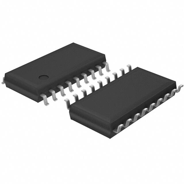
Package
SOP18
W(Typ) x D(Typ) x H(Max)
11.20mm x 7.80mm x 2.01mm
Pin pitch 1.27mm
20V High Rating Process
1 Channel Push-pull Control
Current and Voltage Feedback by Driving
Frequency
Adjustable Soft Start
Adjustable Timer Latch
Under-Voltage Detection for IC’s Power Line
Output Over-Voltage Protection
Output Error Signal from FAIL Terminal
Shift to Save Mode by STB Terminal
Burst Control by External PWM Signal
Analog Dimming by External DC Signal
Conversion Function from Pulse to DC
Applications
Operating Power Supply Voltage Range:
9.0V to 18.0V
Oscillator Frequency:
60kHz (RRT=100kΩ)
Operating Current:
2.3mA (Typ)
Operating Temperature Range:
-40°C to +85°C
e
N co
ew m
m
D
es en
ig de
ns d
f
Features
or
PFC Direct current resonance type
White LED Driver for Large LCD
TV, Computer Display, LCD Backlighting.
Figure. 1 SOP18
Typical Application Circuit
< Primary Side >
VCC
VCC
GND
R
GND
PDIM
PVIN
PDIM
STB
ON/OFF
PWM
PWMIN
ERR
FAIL
GND
FAIL
SS_12
ADIM_11
PWM_IN_10
9_CP
6_IS
7_VS
4_RT
5_FB
3_GND
2_STB
1_VCC
BD9412F
8_PWMCMP
PWM2DC_15
COMPSD_14
N2_17
PGND_16
FAIL_13
5V
PDIM
N1_18
N
ot
T1
VCC
ON/OFF
< Secondary Side >
PWMIN
Figure. 2 Typical Application Circuit(s)
〇Product structure : Silicon monolithic integrated circuit
.www.rohm.com
© 2015 ROHM Co., Ltd. All rights reserved.
TSZ22111 • 14 • 001
〇This product has no designed protection against radioactive rays
1/24
TSZ02201-0F5F0C100070-1-2
12.Aug.2015 Rev.002
�BD9412F
Contents
General Description ....................................................................................................................................................1
Features .......................................................................................................................................................................1
Applications ................................................................................................................................................................1
Key Specifications ......................................................................................................................................................1
or
Package .......................................................................................................................................................................1
Typical Application Circuit .........................................................................................................................................1
Pin Configuration ........................................................................................................................................................3
e
N co
ew m
m
D
es en
ig de
ns d
f
Physical Dimension and Marking Diagram ..............................................................................................................3
I/O Equivalent Circuits................................................................................................................................................7
Block Diagram .............................................................................................................................................................8
Pin Function Description .........................................................................................................................................10
Detection Condition List of the Protection Functions ..........................................................................................15
Behavior List of the Protect Function ....................................................................................................................15
Application Example ................................................................................................................................................16
Timing Chart ..............................................................................................................................................................17
Operational Notes .....................................................................................................................................................20
Ordering Information ................................................................................................................................................22
Marking Diagrams .....................................................................................................................................................22
Physical Dimension, Tape and Reel Information ...................................................................................................23
N
ot
R
Revision History .......................................................................................................................................................24
www.rohm.com
© 2015 ROHM Co., Ltd. All rights reserved.
TSZ22111 • 15 • 001
2/24
TSZ02201-0F5F0C100070-1-2
12.Aug.2015 Rev.002
�BD9412F
Absolute Maximum Ratings (Ta = 25°C)
Parameter
Symbol
Rating
Unit
VCC
20
V
VSTB,VPWM2DC,VN2,VN1
20
V
VRT,VFB,VIS,VVS,VPWMCMP,
VCP,VPWMIN,VADIM,VSS,
VFAIL,VCOMPSD
5.5
V
Supply Voltage
STB, PWM2DC, N2, N1
Terminal Voltage
RT, FB, IS, VS, PWMCMP, CP,
PWMIN, ADIM, SS, FAIL,
COMPSD Terminal Voltage
Power Dissipation
Pd
Topr
Junction Temperature
Tjmax
Storage Temperature Range
W
-40 to +85
°C
150
°C
-55 to +150
°C
or
Operating Temperature Range
(Note 1)
0.69
Tstg
e
N co
ew m
m
D
es en
ig de
ns d
f
(Note 1) Derating in done 5.5 mW/°C for operating above Ta≥25°C (Mount on 1-layer 70.0mm x 70.0mm x 1.6mm board)
Caution: Operating the IC over the absolute maximum ratings may damage the IC. The damage can either be a short circuit between pins or an open circuit
between pins and the internal circuitry. Therefore, it is important to consider circuit protection measures, such as adding a fuse, in case the IC is operated over
the absolute maximum ratings.
Recommended Operating Conditions (Ta= -40°C to +85°C)
Parameter
Power Supply Voltage
PWMIN Input Frequency Range
Oscillation Frequency
PWM2DC Input Voltage Range
ADIM Input Voltage Range
ADIM Range with Linearity IS
Symbol
Range
Unit
VCC
9.0 to 18.0
V
fPWMIN
60 to 500
Hz
fOUT
30 to 300
kHz
fPWM2DC
0.09 to 30
kHz
VADIM
0 to 5
V
VADIMLIN
0.5 to 2.1
V
Symbol
Range
Unit
RRT
20 to 200
kΩ
External Components Recommended Range (Ta= -40°C to +85°C)
Parameter
RT Connection Resistance
CP Connection Capacitance
0.01 to 2.2
(Note 2)
µF
CADIM
0.22 to 10
(Note 2)
µF
CSS
0.01 to 0.1
(Note 2)
µF
CCP
ADIM Connection Capacitance
SS Connection Capacitance
(Note 2) Please set connection capacitance above Min value of Recommended Range according to temperature characteristic and DC bias characteristic.
Pin Configuration
Physical Dimension and Marking Diagram
PWM_IN_10
ADIM_11
SS_12
FAIL_13
COMPSD_14
PWM2DC_15
PGND_16
N2_17
Product Name
(Max 11.55 (include.BURR))
BD9412F
9_CP
8_PWMCMP
7_VS
6_IS
5_FB
4_RT
3_GND
BD9412F
2_STB
1_VCC
N
ot
N1_18
R
(TOP VIEW)
Lot No.
Figure. 3 Pin Configuration
(UNIT : mm)
PKG : SOP18
Drawing No. : EX115-5001
SOP18(Unit:mm)
Figure. 4 Physical Dimension and Marking Diagram
www.rohm.com
© 2015 ROHM Co., Ltd. All rights reserved.
TSZ22111 • 15 • 001
3/24
TSZ02201-0F5F0C100070-1-2
12.Aug.2015 Rev.002
�BD9412F
Electrical Characteristics (Unless otherwise specified Ta=25°C, VCC=12V)
Parameter
Symbol
Limit
Min
Typ
Max
Unit
Conditions
【Whole Device】
Circuit Current
ICC1
-
2.3
5.0
mA
Circuit Current at Stand-by
ICC2
-
0
20
µA
fOUT=60kHz,
VPWMCOMP=0V
VSTB=0V
STB Pin High Voltage
VSTH
2.0
-
VCC
V
System ON
STB Pin Low Voltage
VSTL
-0.3
-
+0.8
V
【VCC UVLO Block】
VCC Operation Voltage
VVCCUVP
7.5
8.0
8.5
V
VCC UVLO Hysteresis
⊿VVCCUVP
0.37
0.50
0.63
V
VRT
1.05
1.50
1.95
V
PWMIN Pin High Voltage
VPWMINH
1.8
-
5.0
V
PWMIN Pin Low Voltage
VPWMINL
-0.3
-
+0.8
V
ISS
1.5
2.0
2.5
µA
VSSEND
2.30
2.50
2.70
V
VSDON
1.90
2.00
2.10
V
IS Threshold Voltage 1
VIS1
0.466
0.477
0.488
V
IS Threshold Voltage 2
VIS2
0.239
0.250
0.261
V
IS Threshold Voltage 3
VIS3
0.102
0.114
0.126
V
IS Threshold Voltage 4
VVS
1.212
1.250
1.288
V
IS Source Current 1
IIS1
-
-
0.9
µA
VPWMIN=2.5V
IS Source Current 2
IIS2
40
50
60
µA
VPWMIN=0V, VIS=0.8V
VS Source Voltage
IVS
-
-
0.9
µA
IS COMP Detection Voltage 1
VISCOMP1
0.020
0.050
0.080
V
IS COMP Detection Voltage 2
VISCOMP2
0.90
1.00
1.10
V
or
【STB Block】
e
N co
ew m
m
D
es en
ig de
ns d
f
System OFF
【OSC Block】
RT Terminal voltage
【PWMIN Block】
【Soft Start Block】
Setting Current for Soft Start Timer
and COMPSD Timer
VADIM=2.1V,
VPWM2DC=12V
VADIM=1.1V,
VPWM2DC=12V
VADIM=0.5V,
VPWM2DC=12V
IS sweep down
VADIM=0.4V
IS sweep up
N
ot
R
Soft Start Ended Voltage
Setting Voltage for COMPSD
Timer
【Feed Back Block】
www.rohm.com
© 2015 ROHM Co., Ltd. All rights reserved.
TSZ22111 • 15 • 001
4/24
TSZ02201-0F5F0C100070-1-2
12.Aug.2015 Rev.002
�BD9412F
Electrical Characteristics – continued (Unless otherwise specified Ta=25°C, VCC= 12V)
Parameter
Symbol
Limit
Min
Typ
Min
Unit
Conditions
【Output Block】
N1 Output Sink Resistance
RN1SI
1.5
3.0
6.0
Ω
N1Output Source Resistance
RN1SO
4.5
9.0
18.0
Ω
N2 Output Sink Resistance
RN2SI
1.5
3.0
6.0
Ω
N2 Output Source Resistance
RN2SO
4.5
9.0
18.0
Ω
43.0
45.0
47.0
%
tOFF
100
200
400
ns
Output Frequency
【Timer Block】
fOUT
57.9
60.0
62.1
kHz
Setting Voltage for CP Time
VCP
1.90
2.00
2.10
V
Setting Current for CP Time
【ADIM Block】
ICP
0.85
1.00
1.15
µA
ADIM Pin Inflow Current 1
IADIM1
-5
0
+5
µA
ADIM Pin Inflow Current 2
IADIM2
19
28
37
µA
IPWM2DC
4
6
8
µA
VPWM2DCH
1.8
-
5.0
V
VPWM2DCL
-0.3
-
+0.8
V
VPWM2DCZ
7.5
8.0
8.5
V
VCOMPSD
3.88
4.00
4.12
V
RFAIL
-
100
200
Ω
fOUT=60kHz
or
MAX DUTY
N1-N2,N2-N1Dead Time
RRT=100kΩ
e
N co
ew m
m
D
es en
ig de
ns d
f
MAX DUTY
PWM2DC Pin Inflow Current
PWM2DC Pin High Voltage
PWM2DC Pin Low Voltage
PWM2DC Pin Selected Voltage to
High Impedance
VADIM=2.2V,
VPWM2DC=12V
VADIM=5V,
VPWM2DC=12V
VPWM2DC=3V
PWM2DC=sweep up
【COMPSD Block】
COMPSD Detection Voltage
【FAIL Block】
N
ot
R
FAIL Pin ON-Resistance
www.rohm.com
© 2015 ROHM Co., Ltd. All rights reserved.
TSZ22111 • 15 • 001
5/24
TSZ02201-0F5F0C100070-1-2
12.Aug.2015 Rev.002
�BD9412F
Pin Description
Pin No.
Pin Name
IN/OUT
Function
Rating [V]
1
VCC
IN
-0.3 to +20
2
STB
IN
3
GND
IN
4
RT
OUT
5
FB
OUT
6
IS
IN
Power Supply Pin for IC (Built-In UVLO Function)
Power ON/OFF Control Pin for IC
Power OFF when STB=L and Power ON when STB=H.
Ground Pin for Internal Signal in IC
Drive Frequency Setting Pin
Basic Frequency is set by the resistor between RT and
GND and Drive Frequency Modulation Range is set by
the resistor between RT and FB.
Error Amplifier Output pin for LED Current feedback and
LED Voltage feedback
Error Amplifier Input pin for LED Current feedback
7
VS
IN
PWMCMP
IN
CP
OUT
PWMIN
IN
ADIM
IN
SS
OUT
FAIL
OUT
COMPSD
IN
PWM2DC
IN
9
10
11
12
13
14
15
16
17
or
-0.3 to +5.5
-0.3 to +5.5
-0.3 to +5.5
Error Amplifier Input pin for LED Open Voltage feedback
PWM Comparator Input Pin which controls PWM
operation during brightness adjustment.
N1 and N2 output stop when PWMCMP=L, and they
output Max Duty when PWMCMP=H
Timer Latch Setting Pin
In abnormal case, 1µA (Typ) will be charged to the
capacitor connected to CP, and IC becomes latch status
after output operation stops at CP>2V(Typ)
PWM Signal Input Pin for burst brightness adjustment
-0.3 to +5.5
DC Signal Input Pin for analog dimming
Soft Start timer and COMPSD timer Setting Pin
During start-up, 2µA (Typ) will be charged to connected
capacitor. At SS>2.0V(typ), COMPSD can start to
detect. At SS>2.5V (typ), CP can accept charge
operation.
Error Indication Signal Output Pin
Normal : L, Error : Open
Abnormal Over Voltage Detection Pin
When detecting abnormality, output operation stops and
IC becomes latch status after 2 clocks.
Pulse to DC converting pin
Pulse Signal is translated to flat dc level by 100kΩ
resistor in IC and the capacitor connected to ADIM.
Power Ground for external MOSFET drive
-0.3 to +5.5
-0.3 to +5.5
-0.3 to +5.5
-0.3 to +5.5
-0.3 to +5.5
-0.3 to +5.5
-0.3 to +5.5
-0.3 to +20
PGND
IN
N2
OUT
Output pin for external FET drive circuit (Channel N2)
-0.3 to +20
-
N1
OUT
Output pin for external FET drive circuit (Channel N1)
-0.3 to +20
N
ot
R
18
-
e
N co
ew m
m
D
es en
ig de
ns d
f
8
-0.3 to +20
www.rohm.com
© 2015 ROHM Co., Ltd. All rights reserved.
TSZ22111 • 15 • 001
6/24
TSZ02201-0F5F0C100070-1-2
12.Aug.2015 Rev.002
�BD9412F
I/O Equivalent Circuits
STB
RT
VCC
FB
REF
REF
REF
VCC
160KΩ
STB
10KΩ
300KΩ
20Ω
FB
RT
130KΩ
50KΩ
GND GND
GND
GND
GND
GND
IS
GND
GND
REF
REF
REF
REF
REF
REF
REF
PWMCMP
20Ω
100KΩ
1KΩ
GND
PWMCMP
e
N co
ew m
m
D
es en
ig de
ns d
f
VS
REF
VCC
or
GND
VS
IS
100kΩ
10KΩ
10KΩ
GND
GND
GND
GND
GND
CP
REF
GND
GND
GND
GND
GND
PWMIN
GND
GND
ADIM
2.2V
VCC
REF
VCC
100KΩ
PWMIN
CP
100KΩ
ADIM
GND
GND
GND
GND
SS
REF
50Ω
ot
GND
GND
GND
N
GND
GND
REF
GND
N2
REF
VCC
GND
VCC
N1
90KΩ
GND
PGND
PGND
GND
VCC
N2
100KΩ
GND
GND
N1
VCC
400KΩ
100KΩ
100KΩ
COMP
GND
REF
GND
GND
COMPSD
FAIL
SS
PWM2DC
PWM2DC
GND
VCC
350Ω
GND
GND
GND
FAIL
R
REF
REF
100KΩ
350Ω
GND
GND
PGND
90KΩ
PGND
PGND
PGND
Figure. 5 I/O equivalent circuit
www.rohm.com
© 2015 ROHM Co., Ltd. All rights reserved.
TSZ22111 • 15 • 001
7/24
TSZ02201-0F5F0C100070-1-2
12.Aug.2015 Rev.002
�BD9412F
Block Diagram
VCC
VCC
RT
PWMIN
UVLO
OSC
BLOCK
PWM
STB
STB
BLOCK
SYSTEM
BLOCK
ON / OFF
e
N co
ew m
m
D
es en
ig de
ns d
f
CT
or
BLOCK
VCC
FB
IS
N1
Feedback
VS
BLOCK
SS
LOGIC
BLOCK
CT
ADIM
PWM2DC
GND
BLOCK
PWM
BLOCK
PWMCMP
DR V
Analog
Dimming
N2
PGND
PROTECT
BLOCK
CP
FAIL
Figure. 6 Block Diagram
N
ot
R
COMPSD
www.rohm.com
© 2015 ROHM Co., Ltd. All rights reserved.
TSZ22111 • 15 • 001
8/24
TSZ02201-0F5F0C100070-1-2
12.Aug.2015 Rev.002
�BD9412F
Typical Performance Curves
5
70
3
2
66
64
62
or
Output
Frequency: f:OUT
fOUT[kHz]
[kHz]
Output
Frequency
4
1
VCC=12V
RRT=100kΩ
68
60
58
e
N co
ew m
m
D
es en
ig de
ns d
f
Operating
Current
: ICC[mA]
[mA]
Operating
Current
: ICC1
Ta=25°C
56
54
52
50
0
8
10
12
14
Supply
Voltage
Supply
Voltage: V: CC
Vcc[V]
[V]
16
-40
18
100
1.0
50
VCC=12V
RRT=100kΩ
VPWMCMP=OPEN
ot
R
46
Ta=25°C
VCC=12V
0.8
Voltage: VIS
: VIS[V]
[V]
ISIS
Voltage
48
MAX
DUTY
[%]
Max Duty
: [%]
0
20
40
60
80
Temperature
: Ta [°C]
Temperature
: Temp.
[℃]
Figure 8. Output Frequency vs Temperature
Figure 7. Operating Current vs Power Supply Voltage
44
-20
0.6
0.4
0.2
N
42
0.0
40
-40
-20
0
20
40
60
Temperature
: Ta [°C]
Temperature
: Temp
[deg]
80
100
Figure 10. IS Voltage vs ADIM Voltage
Figure 9. MAX DUTY vs Temperature
www.rohm.com
© 2015 ROHM Co., Ltd. All rights reserved.
TSZ22111 • 15 • 001
0.0 0.5 1.0 1.5 2.0 2.5 3.0 3.5 4.0 4.5 5.0
ADIMVoltage
Voltage::VVADIM
[V]
ADIM
ADIM [V]
9/24
TSZ02201-0F5F0C100070-1-2
12.Aug.2015 Rev.002
�BD9412F
Pin Function Description
PIN.1 VCC
This is power supply pin for the IC. Normal operation range (Typ) is from 9V to 18V. Please place ceramic
capacitor bigger than 0.1µF as bypass capacitor between VCC and GND. It is for noise elimination.
or
PIN.2 STB
This PIN is for setting of ON/OFF. It is possible to use as reset when shutting down.
Please set the STB terminal voltage below VCC voltage. In addition, please set below 4V if the voltage is applied
earlier than VCC.
Depending on input voltage to STB pin, the status of IC might be switched (ON/OFF). Please avoid using between
the two status (0.8V to 2.0V)
e
N co
ew m
m
D
es en
ig de
ns d
f
PIN.3 GND
This is signal system GND for IC inside. Please make it independent from PGND as much as possible (We
recommend this because it has less influence with switching noise which comes from short circuit of PGND and
GND at connector close to GND pin.
Vin
GND_PIN
IC
PGND
N1
N2
GND
Figure. 11
PIN.4 RT
Set up the charge/discharge current by frequency of IC inside.
By changing the resistance value of resistor between RT pin and GND, it is possible to set up basic drive
frequency as following formula;
Basic frequency means output N1, N2 frequency which is determined only with resistor between RT pin and GND.
6000
[kHz]
RRT [k]
( f OUT 200kHz)
f OUT
6673
[kHz]
RRT [k] 3.336
( f OUT 200kHz)
1,000
Out put Frequency : f OUT [ k Hz]
N
ot
R
f OUT
100
10
1
10
100
1,000
RT Resistance : RRT [kΩ]
Figure. 12 RT Resistance vs Output Frequency
There is a discrepancy between theoretical formula and actual device. For frequency setting, please thoroughly
verify it with actual application. In addition, frequency may change upon resistor RADJ which is placed between
RT and FB pins
www.rohm.com
© 2015 ROHM Co., Ltd. All rights reserved.
TSZ22111 • 15 • 001
10/24
TSZ02201-0F5F0C100070-1-2
12.Aug.2015 Rev.002
�BD9412F
PIN.5 FB
This is output pin for LED current feedback (IS pin) error amplifier and open LED voltage feedback (VS pin) error
amplifier. The capacitance between FB and IS (1500pF to 0.01µF) also determines start up time of LED current
necessary during phase compensation and brightness adjustment. Capacitance between FB and VS (1500pF to
0.01µF) is for phase compensation of error amplifier.
Moduration width of Output Frequency
As shown by left graph, by changing resistor RADJ
between RB and RT, it is possible to determine the
modulation width of frequency.
or
125
108.1
100
Modulation width of frequency determined by the
resistor between RB and RT resistor (Theoretical
formula : Example)
When RADJ=100kΩ , Δ fOUT=108.1kHz
75
50
e
N co
ew m
m
D
es en
ig de
ns d
f
Modulation width of Output Frequency: Δf
OUT
[kHz]
150
Figure. xx
25
0
10
100
Figure. 13
1000
RADJ Resistance
ADJ [kΩ]
出力周波数変動幅
対: RR
ADJ 抵抗値
特性
Figure. 13 Modulation width of Output Frequency vs RADJ Resistance
Output Frequency vs FB Voltage
200
180
167.8
140
Modulation width of frequency determined by the
resistor between RB and RT resistor (Theoretical
formula : Example)
When RADJ=100kΩ , Δ fOUT=108.1kHz
120
100
80
60
R
Output Frequency : fOUT [kHz]
160
40
20
3.2
ot
0.5
0
N
0
59.7
1
2
3
4
5
6
FB Voltage : VFB [V]
Figure. 14 Output Frequency vs FB Voltage
The basic drive frequency is determined by resistor R RT which is connected from RT pin to GND. The basic
frequency is the one at VFB=1.5V, and operation frequency range will be fixed with frequency modulation width that
is determined by RADJ under this condition. When RRT=51kΩ, fOUT=127.7kHz becomes to basic drive frequency.
www.rohm.com
© 2015 ROHM Co., Ltd. All rights reserved.
TSZ22111 • 15 • 001
11/24
TSZ02201-0F5F0C100070-1-2
12.Aug.2015 Rev.002
�BD9412F
PIN.6 IS
This is input pin of LED current feedback (IS pin) error amplifier. Please set up as normal voltage (ADIM/4.4)V
(Typ). When IS pin voltage becomes less than (ADIM/8.8)V (Typ) or higher than 1.0V, the output will be stopped
and latched.
or
50uA
e
N co
ew m
m
D
es en
ig de
ns d
f
FB
R2
R1
IS
_
12kΩ
+
ADIM
Error Amp
Gain
1/4.4
Figure. 15 IS Block Diagram
50µA (Typ) current flows from IS pin to external resistor during OFF period of burst brightness adjustment.
Considering Min value of IS source current during burst brightness adjustment, please set that total resistance
from IS Pin to GND is from 8kΩ to 22kΩ. When R2 is 12kΩ in above diagram, please set 8kΩ < R1 + R2 < 22Kω
PIN.7 VS
This is input pin of Open LED voltage feedback (VS pin) error amplifier. It has to be 1.25V during LED is open.
When LED is ON, it will be 0.5V to 1.0V. When VS pin becomes over 1.25V, protection circuit will start operation,
and if it becomes more than CP timer set up time (Timer Latch), it will shut down.
Connector
8
7
6
5
N
ot
R
FB
R1
VS
R2
R3
Error Amp
_
+
1. 25 V
Figure. 16 VS Block Diagram
Please set C1, C2, R1, R2, and R3 value to input 1.25V to VS pin during LED bar’s connector disconnects.
PIN.8 PWMCMP
PWMCOMP pin voltage is fixed by DUTY of drive output N1, N2 in comparison with a saw wave of IC inside. This
pin has 100µA sink/source current capability and when external capacitor is connected between PWMCMP and
GND, IC will operate PWM at brightness start up stage. When N1 and N2 only drive at MaxDuty, please set
PWMCMP=open.
www.rohm.com
© 2015 ROHM Co., Ltd. All rights reserved.
TSZ22111 • 15 • 001
12/24
TSZ02201-0F5F0C100070-1-2
12.Aug.2015 Rev.002
�BD9412F
PIN.9 CP
This pin sets up the time from the point of abnormal detection till shut down (Timer Latch). Having 1µA constant
current charges at external capacitor connected to CP pin, it will shut down when it becomes over 2.0V. During soft
start, there is no charge to CP external capacitor even fulfilling CP pin charge condition (timer latch). External
capacitor is set around 0.01µF to 2.2µF).
TCP CCP
VCP CCP 2.0
2.0 106 CCP
I CP 1.0 10 6
[sec]
Timer Latch Time TCP
1uA
or
100
1
e
N co
ew m
m
D
es en
ig de
ns d
f
CCP
Timer Latch Time : TCP[sec]
10
Timer latch
Shut-down
2.0V
Timer Start
0.1
0.01
0.001
0.001
0.01
Figure. 17 CP Block Diagram
0.1
1
10
CP Capacitance CCP[µF]
Figure. 18 Timer Latch Time vs CP Capacitance
PIN.10 PWMIN
By inputting PWM pulse signal at PWMIN pin, it is possible to adjust burst brightness. (High level: over 1.8V, Low
level: below 0.8V).
condition
LED condition
PWMIN : 1.8V to 5.0V
Turn On
PWMIN : -0.3V to 0.8V
Turn Off
PIN.11 ADIM
ADIM pin is Input and Output Pin of DC signal for analog dimming. According to ADIM Input level, each pin’s
function is changed as the followings. Pulse-DC translation Circuit is shown in Figure.20.
PWM2DCinput level
-0.3V2.5V
VS < 1.25V
VCC UVLO
VCC
VCC < 8.0V
-
VCC < 7.5V
COMPSD
COMPSD > 4.0V
SS>2.0V
COMPSD < 3.8V
-
e
N co
ew m
m
D
es en
ig de
ns d
f
COMPSD
or
LED OPEN
2CLK
Restart by
release
Latch off
To reset the latch type protection, please set STB logic to ‘L’ once. Otherwise the detection of VCCUVLO is required. The count number in the list is calculated
with double of output frequency.
Behavior List of the Protect Function
Protect Function
Operation of the Protect Function
N1,N2 Output
SS pin
FAIL pin
Stop after latch
Low after latch
High after latch
Stop after latch
Low after latch
High after latch
OVP
Stop after latch
Low after latch
High after latch
VCC UVLO
Stop immediately
Low Immediately
High Immediately
COMPSD
Stop after latch
Low after latch
High after latch
N
ot
R
LED OPEN
LED SHORT
www.rohm.com
© 2015 ROHM Co., Ltd. All rights reserved.
TSZ22111 • 15 • 001
15/24
TSZ02201-0F5F0C100070-1-2
12.Aug.2015 Rev.002
�CN1
ERR
PWMIN
ON/OFF
VCC
PDIM
R_FAILH
R
GND
R_NH1
Q_NH
ZDH
FETH
R_PWMIN1
C_H
T2
R_IS2
R_ISIN
D_VO1
C_VO2
C_VO1
R_VSINL
R_PWMIN
R_STB2
R_STB1
R_N1
C_STB1
SW
T1
R_NL2
D_NL
Q_NL
R_RT
R_FB
BD9412F
5V
FAIL
R_NL1
R_NH2
D_NH
C_ISFB
C_VSFB
ZDL
R_IS
R_VS
R_NL3
FETL
R_NH3
R_PWMCMP
C_CP
R_PWMIN2
C_L
R_IS3
C_ISIN
D_VO2
e
N co
ew m
m
D
es en
ig de
ns d
f
C_VCC
R_VCC
FAIL
PWMIN
PWM
PVIN
N1_18
1_VCC
ON/OFF
N2_17
2_STB
PDIM
PWM2DC_15
4_RT
STB
FAIL_13
PDIM
< Primary Side >
R_FAIL
GND
CN2
C_SS
GND
ot
C_SDON
VCC
R_N2
PGND_16
3_GND
R_CMPSD
COMPSD_14
5_FB
ADIM_11
VCC
SS_12
7_VS
16/24
6_IS
PWM_IN_10
www.rohm.com
© 2015 ROHM Co., Ltd. All rights reserved.
TSZ22111 • 15 • 001
8_PWMCMP
Figure. 23
9_CP
N
R_IIN
< Secondary Side >
or
R_VSINH
BD9412F
Application Example
Introduce an application example with BD9412F
Application Example
TSZ02201-0F5F0C100070-1-2
12.Aug.2015 Rev.002
�BD9412F
Timing Chart
When it Detects Quick Detection Type Error
STB
2.0V
2.5V
2.0V
2.5V
2.0V
2.5V
2.0V
or
SS
e
N co
ew m
m
D
es en
ig de
ns d
f
FB
1.0V
1
ADIM/4.4
IS
2
ADIM/4.4
ADIM/8.8
1.25V
VS
COMPSD
CP
FAIL
1.25V
3
4.0V
2.0V
Figure. 24 Timing Chart 1
R
[The explanation of quick abnormal detection]
Due to the timing of ① to ③ in the above chart, the IC detects malfunction and starts the output-mute latch without CP
Charge . For ① to ③, the malfunction is detected according to the conditions in the table shown below.
Content of Abnormal Detection
Abnormal LED current detection
Abnormal LED short detection
Condition of Abnormal Detection
IS1.0V
③
COMPSD Over Voltage detection
COMPSD≥ 4.0V
N
ot
No.
①
②
www.rohm.com
© 2015 ROHM Co., Ltd. All rights reserved.
TSZ22111 • 15 • 001
17/24
TSZ02201-0F5F0C100070-1-2
12.Aug.2015 Rev.002
�BD9412F
When it Detects Timer Latch Type Error
STB
2.0V
2.5V
2.0V
2.5V
2.0V
or
SS
3.2V
e
N co
ew m
m
D
es en
ig de
ns d
f
FB
1.0V
ADIM/4.4
IS
ADIM/8.8
1.25V
1.25V
4
VS
COMPSD
1.80V
CP
2.0V
FAIL
R
Figure. 25 Timing Chart 2
ot
[The explanation of Time latch type error detection]
Due to the timing of ④ in the above chart, the IC detects abnormal and starts the timer latch charging. For ④, the
abnormal is detected according to the conditions in the table shown below.
N
No.
④
Content of Abnormal Detection
Abnormal LED voltage detection
www.rohm.com
© 2015 ROHM Co., Ltd. All rights reserved.
TSZ22111 • 15 • 001
Condition of Abnormal Detection
VS≥ 1.25V
18/24
TSZ02201-0F5F0C100070-1-2
12.Aug.2015 Rev.002
�BD9412F
Output Timing Chart
BD9412F outputs the signal that operates the Push-Pull or Half-Bridge which is made up of Nch FET. The output timing
of drive signal is shown in the following chart
e
N co
ew m
m
D
es en
ig de
ns d
f
PWMIN
or
CT _ SYNC_ OUT
(can’t see it)
FB
FB=0.5V
Internal CT
( can’t see it)
FB=0.5V
PWMCOMP
CT
N1
VCC
R
N2
Figure. 26 Output Timing Chart
N
ot
VCC
www.rohm.com
© 2015 ROHM Co., Ltd. All rights reserved.
TSZ22111 • 15 • 001
19/24
TSZ02201-0F5F0C100070-1-2
12.Aug.2015 Rev.002
�BD9412F
Operational Notes
Reverse Connection of Power Supply
Connecting the power supply in reverse polarity can damage the IC. Take precautions against reverse polarity when
connecting the power supply, such as mounting an external diode between the power supply and the IC’s power
supply pins.
2.
Power Supply Lines
Design the PCB layout pattern to provide low impedance supply lines. Separate the ground and supply lines of the
digital and analog blocks to prevent noise in the ground and supply lines of the digital block from affecting the analog
block. Furthermore, connect a capacitor to ground at all power supply pins. Consider the effect of temperature and
aging on the capacitance value when using electrolytic capacitors.
3.
Ground Voltage
Ensure that no pins are at a voltage below that of the ground pin at any time, even during transient condition.
4.
Ground Wiring Pattern
When using both small-signal and large-current ground traces, the two ground traces should be routed separately but
connected to a single ground at the reference point of the application board to avoid fluctuations in the small-signal
ground caused by large currents. Also ensure that the ground traces of external components do not cause variations
on the ground voltage. The ground lines must be as short and thick as possible to reduce line impedance.
5.
Thermal Consideration
Should by any chance the power dissipation rating be exceeded the rise in temperature of the chip may result in
deterioration of the properties of the chip. In case of exceeding this absolute maximum rating, increase the board size
and copper area to prevent exceeding the Pd rating.
6.
Recommended Operating Conditions
These conditions represent a range within which the expected characteristics of the IC can be approximately
obtained. The electrical characteristics are guaranteed under the conditions of each parameter.
7.
Inrush Current
When power is first supplied to the IC, it is possible that the internal logic may be unstable and inrush current may
flow instantaneously due to the internal powering sequence and delays, especially if the IC has more than one power
supply. Therefore, give special consideration to power coupling capacitance, power wiring, width of ground wiring,
and routing of connections.
8.
Operation Under Strong Electromagnetic Field
Operating the IC in the presence of a strong electromagnetic field may cause the IC to malfunction.
9.
Testing on Application Boards
When testing the IC on an application board, connecting a capacitor directly to a low-impedance output pin may
subject the IC to stress. Always discharge capacitors completely after each process or step. The IC’s power supply
should always be turned off completely before connecting or removing it from the test setup during the inspection
process. To prevent damage from static discharge, ground the IC during assembly and use similar precautions during
transport and storage.
N
ot
R
e
N co
ew m
m
D
es en
ig de
ns d
f
or
1.
www.rohm.com
© 2015 ROHM Co., Ltd. All rights reserved.
TSZ22111 • 15 • 001
20/24
TSZ02201-0F5F0C100070-1-2
12.Aug.2015 Rev.002
�BD9412F
Operational Notes – continued
10. Inter-pin Short and Mounting Errors
Ensure that the direction and position are correct when mounting the IC on the PCB. Incorrect mounting may result in
damaging the IC. Avoid nearby pins being shorted to each other especially to ground, power supply and output pin.
Inter-pin shorts could be due to many reasons such as metal particles, water droplets (in very humid environment)
and unintentional solder bridge deposited in between pins during assembly to name a few.
or
11. Unused Input Pins
Input pins of an IC are often connected to the gate of a MOS transistor. The gate has extremely high impedance and
extremely low capacitance. If left unconnected, the electric field from the outside can easily charge it. The small
charge acquired in this way is enough to produce a significant effect on the conduction through the transistor and
cause unexpected operation of the IC. So unless otherwise specified, unused input pins should be connected to the
power supply or ground line.
e
N co
ew m
m
D
es en
ig de
ns d
f
12. Regarding the Input Pin of the IC
This monolithic IC contains P+ isolation and P substrate layers between adjacent elements in order to keep them
isolated. P-N junctions are formed at the intersection of the P layers with the N layers of other elements, creating a
parasitic diode or transistor. For example (refer to figure below):
When GND > Pin A and GND > Pin B, the P-N junction operates as a parasitic diode.
When GND > Pin B, the P-N junction operates as a parasitic transistor.
Parasitic diodes inevitably occur in the structure of the IC. The operation of parasitic diodes can result in mutual
interference among circuits, operational faults, or physical damage. Therefore, conditions that cause these diodes to
operate, such as applying a voltage lower than the GND voltage to an input pin (and thus to the P substrate) should
be avoided.
Resistor
Transistor (NPN)
Pin A
Pin B
C
E
Pin A
N
P+
P
N
N
P+
N
Parasitic
Elements
N
P+
N P
N
P+
B
N
C
E
Parasitic
Elements
P Substrate
P Substrate
Parasitic
Elements
Pin B
B
GND
Parasitic
Elements
GND
GND
N Region
close-by
GND
Figure xx. Example of monolithic IC structure
13. Ceramic Capacitor
When using a ceramic capacitor, determine the dielectric constant considering the change of capacitance with
temperature and the decrease in nominal capacitance due to DC bias and others.
Thermal Shutdown Circuit(TSD)
This IC has a built-in thermal shutdown circuit that prevents heat damage to the IC. Normal operation should always
be within the IC’s power dissipation rating. If however the rating is exceeded for a continued period, the junction
temperature (Tj) will rise which will activate the TSD circuit that will turn OFF all output pins. When the Tj falls below
the TSD threshold, the circuits are automatically restored to normal operation.
Note that the TSD circuit operates in a situation that exceeds the absolute maximum ratings and therefore, under no
circumstances, should the TSD circuit be used in a set design or for any purpose other than protecting the IC from
heat damage.
ot
R
14.
N
15. Over Current Protection Circuit (OCP)
This IC incorporates an integrated over current protection circuit that is activated when the load is shorted. This
protection circuit is effective in preventing damage due to sudden and unexpected incidents. However, the IC should
not be used in applications characterized by continuous operation or transitioning of the protection circuit.
www.rohm.com
© 2015 ROHM Co., Ltd. All rights reserved.
TSZ22111 • 15 • 001
21/24
TSZ02201-0F5F0C100070-1-2
12.Aug.2015 Rev.002
�BD9412F
Ordering Information
D
9
4
1
Part Number
2
F
-
Package
F:SOP18
E2
Packaging and forming specification
E2: Embossed tape and reel
or
B
e
N co
ew m
m
D
es en
ig de
ns d
f
Marking Diagrams
SOP18(TOP VIEW)
Part Number Marking
BD9412F
LOT Number
N
ot
R
1PIN MARK
www.rohm.com
© 2015 ROHM Co., Ltd. All rights reserved.
TSZ22111 • 15 • 001
22/24
TSZ02201-0F5F0C100070-1-2
12.Aug.2015 Rev.002
�BD9412F
Physical Dimension, Tape and Reel Information
Package Name
SOP18
e
N co
ew m
m
D
es en
ig de
ns d
f
or
(Max 11.55 (include.BURR))
N
ot
R
(UNIT : mm)
PKG : SOP18
Drawing No. : EX115-5001
www.rohm.com
© 2015 ROHM Co., Ltd. All rights reserved.
TSZ22111 • 15 • 001
23/24
TSZ02201-0F5F0C100070-1-2
12.Aug.2015 Rev.002
�BD9412F
Revision History
Revision No.
001
Date
26.May.2015
Page
All
Changes
New Release
General Description
12.Aug.2015
p.1
N
ot
R
e
N co
ew m
m
D
es en
ig de
ns d
f
or
002
LED Short Detection (IS Low Detection) and LED Open Detection (IS High
Detection).
↓
LED Short Detection (IS High Detection) and LED Open Detection (IS Low
Detection).
www.rohm.com
© 2015 ROHM Co., Ltd. All rights reserved.
TSZ22111 • 15 • 001
24/24
TSZ02201-0F5F0C100070-1-2
12.Aug.2015 Rev.002
�Datasheet
Notice
Precaution on using ROHM Products
Our Products are designed and manufactured for application in ordinary electronic equipments (such as AV equipment,
OA equipment, telecommunication equipment, home electronic appliances, amusement equipment, etc.). If you
(Note 1)
, transport
intend to use our Products in devices requiring extremely high reliability (such as medical equipment
equipment, traffic equipment, aircraft/spacecraft, nuclear power controllers, fuel controllers, car equipment including car
accessories, safety devices, etc.) and whose malfunction or failure may cause loss of human life, bodily injury or
serious damage to property (“Specific Applications”), please consult with the ROHM sales representative in advance.
Unless otherwise agreed in writing by ROHM in advance, ROHM shall not be in any way responsible or liable for any
damages, expenses or losses incurred by you or third parties arising from the use of any ROHM’s Products for Specific
Applications.
or
1.
ROHM designs and manufactures its Products subject to strict quality control system. However, semiconductor
products can fail or malfunction at a certain rate. Please be sure to implement, at your own responsibilities, adequate
safety measures including but not limited to fail-safe design against the physical injury, damage to any property, which
a failure or malfunction of our Products may cause. The following are examples of safety measures:
[a] Installation of protection circuits or other protective devices to improve system safety
[b] Installation of redundant circuits to reduce the impact of single or multiple circuit failure
3.
Our Products are designed and manufactured for use under standard conditions and not under any special or
extraordinary environments or conditions, as exemplified below. Accordingly, ROHM shall not be in any way
responsible or liable for any damages, expenses or losses arising from the use of any ROHM’s Products under any
special or extraordinary environments or conditions. If you intend to use our Products under any special or
extraordinary environments or conditions (as exemplified below), your independent verification and confirmation of
product performance, reliability, etc, prior to use, must be necessary:
[a] Use of our Products in any types of liquid, including water, oils, chemicals, and organic solvents
[b] Use of our Products outdoors or in places where the Products are exposed to direct sunlight or dust
[c] Use of our Products in places where the Products are exposed to sea wind or corrosive gases, including Cl2,
H2S, NH3, SO2, and NO2
[d] Use of our Products in places where the Products are exposed to static electricity or electromagnetic waves
[e] Use of our Products in proximity to heat-producing components, plastic cords, or other flammable items
[f] Sealing or coating our Products with resin or other coating materials
[g] Use of our Products without cleaning residue of flux (even if you use no-clean type fluxes, cleaning residue of
flux is recommended); or Washing our Products by using water or water-soluble cleaning agents for cleaning
residue after soldering
[h] Use of the Products in places subject to dew condensation
4.
The Products are not subject to radiation-proof design.
5.
Please verify and confirm characteristics of the final or mounted products in using the Products.
6.
In particular, if a transient load (a large amount of load applied in a short period of time, such as pulse. is applied,
confirmation of performance characteristics after on-board mounting is strongly recommended. Avoid applying power
exceeding normal rated power; exceeding the power rating under steady-state loading condition may negatively affect
product performance and reliability.
7.
De-rate Power Dissipation (Pd) depending on Ambient temperature (Ta). When used in sealed area, confirm the actual
ambient temperature.
8.
Confirm that operation temperature is within the specified range described in the product specification.
9.
ROHM shall not be in any way responsible or liable for failure induced under deviant condition from what is defined in
this document.
ot
R
2.
N
e
N co
ew m
m
D
es en
ig de
ns d
f
(Note1) Medical Equipment Classification of the Specific Applications
JAPAN
USA
EU
CHINA
CLASSⅢ
CLASSⅡb
CLASSⅢ
CLASSⅢ
CLASSⅣ
CLASSⅢ
Precaution for Mounting / Circuit board design
1.
When a highly active halogenous (chlorine, bromine, etc.) flux is used, the residue of flux may negatively affect product
performance and reliability.
2.
In principle, the reflow soldering method must be used on a surface-mount products, the flow soldering method must
be used on a through hole mount products. If the flow soldering method is preferred on a surface-mount products,
please consult with the ROHM representative in advance.
For details, please refer to ROHM Mounting specification
Notice-PGA-E
© 2015 ROHM Co., Ltd. All rights reserved.
Rev.001
�Datasheet
Precautions Regarding Application Examples and External Circuits
If change is made to the constant of an external circuit, please allow a sufficient margin considering variations of the
characteristics of the Products and external components, including transient characteristics, as well as static
characteristics.
2.
You agree that application notes, reference designs, and associated data and information contained in this document
are presented only as guidance for Products use. Therefore, in case you use such information, you are solely
responsible for it and you must exercise your own independent verification and judgment in the use of such information
contained in this document. ROHM shall not be in any way responsible or liable for any damages, expenses or losses
incurred by you or third parties arising from the use of such information.
Precaution for Electrostatic
or
1.
e
N co
ew m
m
D
es en
ig de
ns d
f
This Product is electrostatic sensitive product, which may be damaged due to electrostatic discharge. Please take proper
caution in your manufacturing process and storage so that voltage exceeding the Products maximum rating will not be
applied to Products. Please take special care under dry condition (e.g. Grounding of human body / equipment / solder iron,
isolation from charged objects, setting of Ionizer, friction prevention and temperature / humidity control).
Precaution for Storage / Transportation
1.
Product performance and soldered connections may deteriorate if the Products are stored in the places where:
[a] the Products are exposed to sea winds or corrosive gases, including Cl2, H2S, NH3, SO2, and NO2
[b] the temperature or humidity exceeds those recommended by ROHM
[c] the Products are exposed to direct sunshine or condensation
[d] the Products are exposed to high Electrostatic
2.
Even under ROHM recommended storage condition, solderability of products out of recommended storage time period
may be degraded. It is strongly recommended to confirm solderability before using Products of which storage time is
exceeding the recommended storage time period.
3.
Store / transport cartons in the correct direction, which is indicated on a carton with a symbol. Otherwise bent leads
may occur due to excessive stress applied when dropping of a carton.
4.
Use Products within the specified time after opening a humidity barrier bag. Baking is required before using Products of
which storage time is exceeding the recommended storage time period.
Precaution for Product Label
QR code printed on ROHM Products label is for ROHM’s internal use only.
Precaution for Disposition
When disposing Products please dispose them properly using an authorized industry waste company.
Precaution for Foreign Exchange and Foreign Trade act
Since concerned goods might be fallen under listed items of export control prescribed by Foreign exchange and Foreign
trade act, please consult with ROHM in case of export.
All information and data including but not limited to application example contained in this document is for reference
only. ROHM does not warrant that foregoing information or data will not infringe any intellectual property rights or any
other rights of any third party regarding such information or data.
ot
1.
R
Precaution Regarding Intellectual Property Rights
ROHM shall not have any obligations where the claims, actions or demands arising from the combination of the
Products with other articles such as components, circuits, systems or external equipment (including software).
3.
No license, expressly or implied, is granted hereby under any intellectual property rights or other rights of ROHM or any
third parties with respect to the Products or the information contained in this document. Provided, however, that ROHM
will not assert its intellectual property rights or other rights against you or your customers to the extent necessary to
manufacture or sell products containing the Products, subject to the terms and conditions herein.
N
2.
Other Precaution
1.
This document may not be reprinted or reproduced, in whole or in part, without prior written consent of ROHM.
2.
The Products may not be disassembled, converted, modified, reproduced or otherwise changed without prior written
consent of ROHM.
3.
In no event shall you use in any way whatsoever the Products and the related technical information contained in the
Products or this document for any military purposes, including but not limited to, the development of mass-destruction
weapons.
4.
The proper names of companies or products described in this document are trademarks or registered trademarks of
ROHM, its affiliated companies or third parties.
Notice-PGA-E
© 2015 ROHM Co., Ltd. All rights reserved.
Rev.001
�Datasheet
General Precaution
1. Before you use our Pro ducts, you are requested to care fully read this document and fully understand its contents.
ROHM shall n ot be in an y way responsible or liabl e for fa ilure, malfunction or acci dent arising from the use of a ny
ROHM’s Products against warning, caution or note contained in this document.
2. All information contained in this docume nt is current as of the issuing date and subj ect to change without any prior
notice. Before purchasing or using ROHM’s Products, please confirm the la test information with a ROHM sale s
representative.
The information contained in this doc ument is provi ded on an “as is” basis and ROHM does not warrant that all
information contained in this document is accurate an d/or error-free. ROHM shall not be in an y way responsible or
liable for an y damages, expenses or losses incurred b y you or third parties resulting from inaccur acy or errors of or
concerning such information.
N
ot
R
e
N co
ew m
m
D
es en
ig de
ns d
f
or
3.
Notice – WE
© 2015 ROHM Co., Ltd. All rights reserved.
Rev.001
�