Datasheet
LED Drivers for LCD Backlights
White LED Driver for large LCD Panels
(DCDC Converter Type)
BD9421F
General Description
Key Specifications
BD9421F is high efficiency driver for white LED. This is
designed for large sized LCD. BD9421F is built-in
DCDC converters that supply appropriate voltage for
light source.
BD9421F is also built-in protection function for
abnormal state such as OVP: over voltage protection,
OCP: over current limit protection of DCDC, SCP: short
circuit protection, open detection of LED string.
Thus this is used for conditions of large output voltage
and load conditions.
VCC Supply Voltage Range:
9.0V to 35.0V
DCDC Oscillation Frequency: 150kHz(RT=100kΩ)
Operation Circuit Current:
5mA(Typ)
Operating Temperature Range:
-40°C to +85°C
Applications
LED driver for TV, Monitor and LCD Back Light
Package
W(Typ) x D(Typ) x H(Max)
15.00mm x 7.80mm x 2.01mm
Pin Pitch 1.27mm
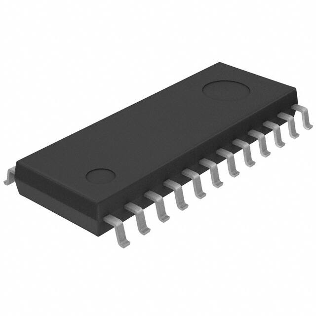
SOP24
Features
6ch LED constant current driver(External PNP Tr
Type)
Maximum LED setting current 500mA(VREF Pin
setting)
±2% LED current accuracy(VREF=0.9V setting)
Built-in DC/DC converter
Analog Dimming(Linear) function
LED protection function(OPEN/SHORT
protection)[PWM-independent Type]
Individual detection and individual LED OFF for both
OPEN and SHORT circuit
VOUT Over Voltage Protection(OVP) and reduced
voltage protection(SCP) circuit
Built-in under voltage lockout function(UVLO) and
over voltage protection(OVP)
Built-in VOUT discharge circuit while shutdown
Figure 1. SOP24
Typical Application Circuit
STB
PWM
REG75
N
PGND
CS
OVP
STB
BSx
PWM
VCC
AGND
RT
FB
VREF
CLx
FAIL
VREF
Figure 2. Typical Application Circuit
〇Product structure : Silicon monolithic integrated circuit
.www.rohm.com
© 2013 ROHM Co., Ltd. All rights reserved.
TSZ22111 • 14 • 001
〇This product has no designed protection against radioactive rays
1/27
TSZ02201-0F1F0C100310-1-2
25.Sep.2015 Rev.003
�Datasheet
BD9421F
Absolute Maximum Ratings(Ta = 25°C)
Parameter
Symbol
Rating
Unit
VCC
-0.3 to +36
V
STB,OVP
-0.3 to +36
V
BS1-6
-0.3 to +60
V
CS,CL1-6,FB,RT
-0.3 to +7
V
REG75,N
-0.3 to +14
V
PWM,VREF
-0.3 to +20
V
Supply Voltage
STB,OVP Voltage
BS1-6 Voltage
CS,CL1-6,FB,RT Voltage
REG75,N Voltage
PWM,VREF Voltage
0.68
(Note 1)
W
Power Dissipation for SOP24
Pd
Operating Temperature Range
Topr
-40 to +85
°C
Storage Temperature Range
Tstg
-55 to +150
°C
Maximum Junction Temperature
Tjmax
150
°C
(Note 1) Derating in done 5.5mW/°C for operating above Ta≧25°C (Mount on 1-layer 70.0mm x 70.0mm x 1.6mm board)
Caution: Operating the IC over the absolute maximum ratings may damage the IC. The damage can either be a short circuit between pins or an open circuit
between pins and the internal circuitry. Therefore, it is important to consider circuit protection measures, such as adding a fuse, in case the IC is operated over
the absolute maximum ratings.
Recommended Operating Conditions(Ta= -40°C to +85°C)
Parameter
Symbol
Min
Typ
Max
Unit
VCC
9
24
35
V
DC/DC Oscillation Frequency
FSW
100
-
800
kHz
Analog Dimming Setting Input Range
VREF
0.6
0.9
3.0
V
Supply Voltage
External Component Recommended Range
Parameter
VCC pin connecting capacity
REG75 pin connecting capacity
RT pin connection resistance range
Symbol
Specification
Unit
CVCC
1 to 100
uF
C_REG
1.0 to 10
uF
RRT
18.75 to 150
kΩ
The operating conditions listed above are constants for the IC alone. To make constant setting with practical set devices, utmost attention should be paid.
Pin Configuration
Marking Diagram and Physical Dimension
(TOP VIEW)
BD9421F
1PIN MARK
LOT No.
SOP24
Figure 3. Pin Configuration
www.rohm.com
© 2013 ROHM Co., Ltd. All rights reserved.
TSZ22111 • 15 • 001
Figure 4. Physical Dimension
2/27
TSZ02201-0F1F0C100310-1-2
25.Sep.2015 Rev.003
�Datasheet
BD9421F
Electrical Characteristics(Unless otherwise specified VCC=24V Ta=25°C)
Parameter
Symbol
Limit
Min.
Typ.
Max.
Unit
Condition
[Whole Device]
Operation Current
ICC
-
5
10
mA
VSTB=3V
Standby Current
IST
-
40
80
uA
VSTB=0V
Operation Voltage (VCC)
VUVLO_VCC
6.5
7.5
8.5
V
VCC=SWEEP UP
Hysteresis Voltage (VCC)
VUHYS_VCC
150
300
600
mV
VCC=SWEEP DOWN
VEAMP
0.55
0.60
0.65
V
BSx pin, VREF=0.9V
FCT
142.5
150.0
157.5
kHz
RT=100kΩ
NMAX_DUTY
90
95
99
%
RT=100kΩ
N Pin Source ON Resistance
RNSO
2.5
5
10
Ω
N Pin Sink ON Resistance
RNSI
2
4
8
Ω
RT Pin Voltage
VRT
1.60
2.00
2.40
V
RT=100kΩ
RT_DET
-0.3
-
VRTx90%
V
RT=SWEEP DOWN
RT Pin Low Resistance
RRT_L
-
2.0
4.0
kΩ
FB Pin Source Current
IFBSO
-115
-100
-85
uA
FB Pin Sink Current
IFBSI
85
100
115
uA
VSTB=0V
VBSx=0V, VREF=0.9V,
VFB=1.0V
VBSx=2.0V, VREF=0.9V,
VFB=1.0V
Over Current Detect Voltage
VCS
0.35
0.40
0.45
V
CS=SWEEP UP
CS Source Current
ICS
15
30
60
uA
VCS=0V
OVP High Detect Voltage
VOVPH
2.88
3.00
3.12
V
VOVP SWEEP UP
OVP Hysteresis Voltage
VOVPH_HYS
150
200
250
V
VOVP SWEEP DOWN
VSCP
0.05
0.10
0.15
V
VOVP SWEEP DOWN
OVP_LK
-2
0
2
uA
VOVP=4V
VCL
294.0
300.0
306.0
mV
VREF=0.9V
VCLMAX
-3%
1.0
+3%
V
VREF max=3.0V
VCLMIN
-3%
200.0
+3%
mV
VREF min=0.6V
RBS
55
80
120
Ω
PWM=High, VCL=Low
VREF_LK
-2
0
2
uA
VREF=1V
[UVLO Block]
[DC/DC Block]
Error amp Base Voltage
Oscillation Frequency
N Pin MAX DUTY Output
RT Short Protection Range
[DC/DC Protection Block]
Short Protection Detect Voltage
OVP Pin Leakage Current
[LED PNP Driver Block]
CL Pin Current Setting Voltage
CL Pin Current Setting Voltage
(Analog MAX)
CL Pin Current Setting Voltage
(Analog MIN)
PNP Driver Output Sink
Resistance
VREF Pin Leakage Current
www.rohm.com
© 2013 ROHM Co., Ltd. All rights reserved.
TSZ22111 • 15 • 001
3/27
TSZ02201-0F1F0C100310-1-2
25.Sep.2015 Rev.003
�Datasheet
BD9421F
Electrical Characteristics(Unless otherwise specified VCC=24V Ta=25°C)
Parameter
Symbol
Limit
Unit
Condition
Min.
Typ.
Max.
VOPEN
0.05
0.10
0.15
V
BSx=SWEEP DOWN
VLSP
8.5
9.0
9.5
V
BSx=SWEEP UP
VCLLVP
0.05
0.10
0.15
V
[LED Protection Block]
LED OPEN Detect Voltage
LED SHORT Detect Voltage
CL Pin Low Detect Voltage
[REG75 Block]
REG75 Output Voltage
REG75
7.425
7.50
7.575
V
REG75 MAX Output Current
| IREG75 |
10
-
-
mA
Io=0mA
REG75_UVLO Detect Voltage
REG75_TH
3.6
4.0
4.4
V
REG75_UVLO Hysteresis
REG75_HYS
250
500
750
mV
REG75 Discharge Resistance
REG75_DIS
0.65
1.00
1.35
MΩ
STB Pin High Voltage
STBH
2.0
-
VCC
V
STB=SWEEP UP
STB Pin Low Voltage
STBL
-0.3
-
0.8
V
STB=SWEEP DOWN
STB Pin Pull Down Resistance
RSTB
600
1000
1400
kΩ
STB=3.0V
PWM Pin High Detect Voltage
PWM_H
1.5
-
18
V
PWM=SWEEP UP
PWM Pin Low Detect Voltage
PWM_L
-0.3
-
0.8
V
PWM=SWEEP DOWN
PWM Pin Pull Down Resistance
RPWM
300
500
700
kΩ
PWM=3.0V
REG75=SWEEP DOWN
STB=ON->OFF,
REG75=SWEEP UP
STB=ON->OFF,
REG75=7.5V
[STB Block]
[PWM Input Block]
www.rohm.com
© 2013 ROHM Co., Ltd. All rights reserved.
TSZ22111 • 15 • 001
4/27
TSZ02201-0F1F0C100310-1-2
25.Sep.2015 Rev.003
�Datasheet
BD9421F
Pin Descriptions
Pin No.
Pin Name
Function
1
REG75
2
N
3
PGND
4
CS
DCDC external NMOS current monitor pin
5
FB
DCDC phase-compensation pin
6
VREF
7
BS1
PNP Tr Base connecting pin1
8
BS2
PNP Tr Base connecting pin2
7.5V regulator output for N output pin
DC/DC switching output pin
Power GND
LED voltage setting pin
9
BS3
PNP Tr Base connecting pin3
10
BS4
PNP Tr Base connecting pin4
11
BS5
PNP Tr Base connecting pin5
12
BS6
PNP Tr Base connecting pin6
13
CL6
PNP Tr collector ・current detection pin6
14
CL5
PNP Tr collector ・current detection pin5
15
CL4
PNP Tr collector ・current detection pin4
16
CL3
PNP Tr collector ・current detection pin3
17
CL2
PNP Tr collector ・current detection pin2
18
CL1
PNP Tr collector ・current detection pin1
19
PWM
Dimming signal input pin
20
OVP
Overvoltage protection detection pin
21
RT
22
AGND
23
STB
Enable pin
24
VCC
Power supply pin
www.rohm.com
© 2013 ROHM Co., Ltd. All rights reserved.
TSZ22111 • 15 • 001
DCDC frequency setting resistor connection pin
Analog GND
5/27
TSZ02201-0F1F0C100310-1-2
25.Sep.2015 Rev.003
�Datasheet
BD9421F
Block Diagram
Vo
VIN
+
CIN
OVP
REF4V
OVP
UVLO
(VCC)
VCC
Protection
STB
REG75
VREG
TSD
OPEN
SHORT
Detect
CP counter
OCP
・・・
REG75
OSC CLK
Control Logic
RT
N
OSC
PGND
CS
ERROR
OSC CLK
PGND
Soft Start
SS counter
-
AGND
-
FB
ERR
AMP
RFB
CFB
+
VREF*2/3
1/10
+
Comp
REF4V
・・・
+
+
SHORT_DET
1/10
+
-
0.9V
0.9V
OPEN_DET
Comp
REG75
+
0.1V
Analog
1/3
VREF
Dimming
PWM
Figure 5. Blockdiagram
www.rohm.com
© 2013 ROHM Co., Ltd. All rights reserved.
TSZ22111 • 15 • 001
6/27
TSZ02201-0F1F0C100310-1-2
25.Sep.2015 Rev.003
�Datasheet
BD9421F
Pin ESD Type
REG75 / N / PGND / CS
PWM
FB
STB
VREF
BS(1-6) / CL(1-6)
OVP
RT
OVP
Figure 6. Pin ESD Type
www.rohm.com
© 2013 ROHM Co., Ltd. All rights reserved.
TSZ22111 • 15 • 001
7/27
TSZ02201-0F1F0C100310-1-2
25.Sep.2015 Rev.003
�Datasheet
BD9421F
Description of pin function
P in 1: REG75
The REG pin is used in the DC/DC converter driver block to output 7.5V power. The maximum operating current is 10mA.
Using the REG pin at a current higher than 10mA can affect the N pin output pulse, causing the IC to malfunction and
leading to heat generation of the IC itself. To avoid this problem, it is recommended to make load setting to the minimum
level.
Pin 2:N
The N pin is used to output power to the external NMOS gate driver for the DC/DC converter in the amplitude range of
approx. 0 to 7.5V. Frequency setting can be made with a resistor connected to the RT pin. For details of frequency
setting, refer to the description of the <RT pin>.
Pin 3: PGND
The PGND pin is a power ground pin for the driver block of the N output pin.
Pin 4: CS
CS pin is current detect for DC/DC current mode inductor current control pin.
Current flowing through the inductor is converted into voltage by the current sensing resistor RCS connected to the CS
pin and this voltage is compared with voltage set with the error amplifier to control the DC/DC output voltage.
The CS pin also incorporates the overcurrent protection (OCP) function. If the CS pin voltage reaches 0.4V (Typ.) or
more, switching operation will be forcedly stopped.
Pin 5: FB
Current mode control DC/DC converter error amplifier output pin. By monitoring voltage of BS(1~6)pin, the highest Vf of
LED column will set 2/3(typ.) of applied VREF voltage to BS pin voltage to control inductor current.
The phase compensation setting has described separately.
In addition, PWM pin will become High Impedance when all PWM signals are in low state, and will maintain FB voltage.
Pin 6: VREF
LED current setting pin.1/3(typ) of applied voltage to VREF pin will be LED current
feedback voltage, 2/3(typ.) of its voltage will be DCDC feedback voltage(the
lowest BSx pin feedback voltage).
Basically, because high accuracy of resistor divider is inputted to VREF pin
externally, the IC internally will be OPEN(High Impedance)state. Please use
external power to design it. It cannot be used in OPEN state.
Pin 7-12: BS1-BS6
LED DRIVER output pin. Please connect to Base Terminal of external PNP Tr.
Pin 13-18: CL6 – CL1
LED current detect pin. By monitoring voltage of CLx pin to detect LED current.
Please connect resistor to collector pin of external PNP Tr. CLx pin of no use channel set CLx>3.3V.
Pin 19: PWM
ON/OFF terminal of LED driver pin. It inputs PWM dimming signal directly to adjust output DUTY dimming.
High/Low level of PWM terminal is shown as follows:
State
PWM Voltage
LED ON state
PWM= 1.5V~18.0V
LED OFF state
PWM= -0.3V~0.8V
Pin 20: OVP
The OVP pin is an input pin for overvoltage protection and short circuit protection of DC/DC output voltage. When voltage
of it over 3.0V or higher, CP counting start.
When OVP pin voltage 4count・・・Detect protection because it is out of interval time
Please verify enough to operate narrow PWM.
Figure 13-2. Timing chart of Timer count
www.rohm.com
© 2013 ROHM Co., Ltd. All rights reserved.
TSZ22111 • 15 • 001
14/27
TSZ02201-0F1F0C100310-1-2
25.Sep.2015 Rev.003
�Datasheet
BD9421F
And then mean input current IIN required for the whole system is given
by the following equation.
I IN
V [V ] I OUT [ A]
OUT
[ A]
VIN [V ] [%]
CS
Rcs
IOUT(total)
●Selection of DC/DC Components
OCP setting / DCDC component current tolerance selection guide
The OCP detection function that is one of the functions of the CS pin will stop the DC/DC converter operating if the CS
pin voltage becomes larger than 0.4V.Consequently, it is needed to calculate a peak current flowing through the coil L and
then review the resistance of RCS. Furthermore, a current tolerance for DC/DC components should be larger than that for
peak current flowing through the coil L. The following describes the peak coil current calculation procedure, CS pin
connection resistor RCS selection procedure, and DC/DC component current tolerance selection procedure .
○Peak coil current Ipeak calculation
VOUT
Ripple voltage generated at the CS pin is determined by conditions
L
for DC/DC application components first, Assuming the conditions as
VIN
below:
IL
「output voltage=VOUT[V] 」
「LED total current=IOUT[A] 」
fsw
「DCDC input voltage=VIN[V] 」
「DCDC efficiency=η[%] 」
N
PGND
Further, according to drive operation with the DC/DC converter switching
frequency fsw [Hz], inductor ripple current ΔIL [A] generated at the inductor L (or
H) is given by the following equation.
Δ IL
(VOUT [V ] V IN [V ]) V IN [V ]
[ A]
L[ H ] VOUT [V ] f SW [ Hz ]
As a result, the peak current Ipeak of IL is given by the following equation.
Ipeak I IN [ A]
IL[ A]
2
[ A] (1)
○CS pin connection resistor RCS selection procedure
The current Ipeak flows into RCS to generate voltage.(See the timing
chart shown to the right)The voltage VCSpeak is given by the following
equation.
VCS peak Rcs Ipeak
[V ]
If VCSpeak voltage reaches 0.4V, DC/DC output will stop. Consequently,
to select RCS resistance, the following condition should be met.
Rcs Ipeak [V ] 0.4 [V ]
○DC/DC component current tolerance selection procedure
Iocp current needed for OCP detection voltage CS to reach 0.4V is given
by the following equation:
I OCP
0.4[V ]
[ A] ( 2)
Rcs[ ]
The relation among Ipeak current (Equation (1)), Iocp current (Equation (2)), and Maximum current tolerance for
component should meet the following equation.
I peak I OCP
MAX current tolerance
DC/DC application components including FETs, inductors, and diodes should be selected so that the Equation
shown above will be met.
In addition, it is recommended to use continuous mode in DCDC application. And the lower limit value of coil ripples
current Imin so as to meet the following equation:
I min I IN [ A]
IL[ A]
[ A] 0
2
A failure to meet this condition is referred to as discontinuous mode and this failure may result in an inadequate rise in
output voltage.
www.rohm.com
© 2013 ROHM Co., Ltd. All rights reserved.
TSZ22111 • 15 • 001
15/27
TSZ02201-0F1F0C100310-1-2
25.Sep.2015 Rev.003
�Datasheet
BD9421F
【Setting example】
Output=VOUT[V]=40V
LED 1ch current=120mA, total LED current IOUT[A]=120mA×6ch=0.72A
DCDC input voltage=VIN [V] =24V
DCDC efficiency=η[%]=90%
Mean input current IIN required for the whole system is given by the following equation:
DCDC switching frequency=fsw[Hz]=200kHz
Inductor [H]=33μH
The inductor ripple current ΔIL [A] is given by the following equation:
Δ IL
(VOUT [V ] V IN [V ]) V IN [V ]
( 40[V ] 24[V ]) 24[V ]
1.45 [ A]
L[ H ] VOUT [V ] f SW [ Hz ]
33 10 6 [ H ] 40[V ] 200 10 3 [ Hz ]
As a result, the peak current Ipeak of IL is given by the following equation.
When RCS resistance is set to 0.1ohm, the VCS peak voltage will be given by the following equation:
Consequently, the result meets the condition.
Furthermore, IOCP current at which OCP is detected is given by the following equation:
I OCP
0.4[V ]
4 . 0 [ A]
0.1[ ]
So must select the component of about 5A in order to meet the above result.
I peak I OCP
Max. Current tolerance for component
Particularly, To select DC/DC components, give consideration to IC variations as well as individual component
variations, and then conduct thorough verification on practical systems..
The lower limit value of coil ripple current Imin is given by the following equation, the component will not be put into
discontinuous mode.
I min
I IN [ A]
IL[ A]
[ A] 1. 33[ A] 0. 73[ A] 0. 60[ A]
2
0
※For the selection of DC/DC components, please also consider the inaccuracy of each componentts.
www.rohm.com
© 2013 ROHM Co., Ltd. All rights reserved.
TSZ22111 • 15 • 001
16/27
TSZ02201-0F1F0C100310-1-2
25.Sep.2015 Rev.003
�Datasheet
BD9421F
○Selection of inductor L
The value of inductor has significant influence on the input ripple current. As
shown by Equation (1), the larger the inductor and the higher the switching
frequency, the inductor ripple current ∆IL becomes increasingly lower.
ΔIL
ΔIL
VIN
(VOUT V IN ) V IN
[ A] ・・・・・
(1)
L VOUT f SW
Expressing efficiency as shown by Equation (2), peak input current is given as
Equation (3).
IL
L
VOUT I OUT
・・・・・
(2)
V IN I IN
ΔIL VOUT I OUT
ΔIL
・・・・・
(3)
ILMAX I IN
2
2
VIN
VOUT
Here,
RCS
L:Inductor value[H]
VIN:input voltage[V]
IIN:input current[A]
COUT
VOUT:DC/DC output voltage[V]
IOUT:output total current[A]
FSW:Oscillation frequency[Hz]
Basically, make setting of ∆IL to approximately 30% to 50% of the output load
current.
If a current in excess of the rated current of the inductor applies to the coil, the inductor will cause magnetic
saturation, resulting in efficiency degradation.
Select an inductor with an adequate margin so that peak current will not exceed the rated current of the inductor.
※ To reduce power dissipation from and increase efficiency of inductor, select an inductor with low resistance
component (DCR or ACR).
※
○Selection of output capacitor COUT
VIN
IL
Select a capacitor on the output side taking into account the stability region
of output voltage and equivalent series resistance necessary to smooth
ripple voltage. Note that higher output ripple voltage may result in a drop in
LED pin voltage, making it impossible to supply set LED current.
The output ripple voltage ∆VOUT is given by Equation (4).
ΔVOUT ILMAX R ESR
L
VOUT
1
C OUT
I OUT
1
f SW
[V ] ・・・・・
(4)
Here, RESR Equivalent series resistance of COUT.
RESR
RCS
※
※
COUT
Select capacitor ratings with an adequate margin for output voltage.
To use an electrolytic capacitor, an adequate margin should be provided for permissible current. Particularly to
apply PWM light modulation to LED, note that a current higher than the set LED current transiently flows.
www.rohm.com
© 2013 ROHM Co., Ltd. All rights reserved.
TSZ22111 • 15 • 001
17/27
TSZ02201-0F1F0C100310-1-2
25.Sep.2015 Rev.003
�Datasheet
BD9421F
○Selection of switching MOSFET transistors
There will be no problem for switching MOSFET transistors having absolute maximum rating higher than rated current
of the inductor L and VF higher than “COUT breakdown voltage Rectifier diode”. However, to achieve high-speed
switching, select transistors with small gate capacity (injected charge amount).
Note: Rated current larger than overcurrent protection setting current is recommended.
Note: Selecting transistors with low on resistance can obtain high efficiency.
○Selection of rectifier diodes
Select Schottky barrier diodes having current capability higher than the rated current of the inductor L and inverse
breakdown voltage higher that COUT breakdown voltage, particularly having low forward voltage VF.
○Selection of Load switch MOSFET and soft start function
In usual DC/DC converter, because there is no switching to a path leading from VIN to VOUT resulting in output voltage
is also occurring even if IC is in OFF state. Please insert PMOSFET between VIN and inductor if you want voltage to 0V
until the IC starts to operate. In addition, FAIL pin can be used for driving load switch after confirmed the logic theory,
and the breakdown voltage of drain-source needed to be selected larger than VIN.
Furthermore, if you would like to make soft start function to load switch, please insert a condenser between Gate
and Source.
www.rohm.com
© 2013 ROHM Co., Ltd. All rights reserved.
TSZ22111 • 15 • 001
18/27
TSZ02201-0F1F0C100310-1-2
25.Sep.2015 Rev.003
�Datasheet
BD9421F
●Phase Compensation Setting Procedure
DC/DC converter application for current mode control includes one each of pole fp (phase delay) by CR filer consisting
of output capacitor and output resistor (i.e., LED current) and zero (phase lead) fZ by the output capacitor and capacitor
ESR.
Furthermore, the step-up DC/DC converter includes RHP zero “fZRHP” as the second zero. Since the RHP zero has
phase delay (90) characteristics like the pole, the crossover frequency fc should be set to not more than RHP zero.
VIN
VOUT
L
ILED
VOUT
+
RCS
i.
CFB2
CFB1
Find Pole fp and RHP zero fZRHP of DC/DC converter.
Here,
I LED
[
Hz ]
2 VOUT COUT
ILED =LED Total current[A],
D
f ZRHP
VOUT VIN
VOUT
VOUT (1 D) 2
[
Hz ]
2 L I LED
Find phase compensation to be inserted to error amplifier.(set fc is 1/5 to fZRHP)
R FB1
Here,
iii.
RFB1
COUT
fp
ii.
FB
gm
RESR
f RHZP RCS I LED
[
]
5 f p gm VOUT (1 D)
C FB1
1
[
F ]
2 RFB1 f p
gm 4.0 10 4 [ S ]
Find zero used to compensate ESR (RESR) of COUT (electrolytic capacitor).
C FB 2
RESR C OUT
[
F ]
RFB1
※Even if a ceramic capacitor (RESR of the order of milliohms) for COUT, it is recommended to insert CFB2 for
stable operation.
To improve transient response, it is necessary to increase RFB1 and reduce CFB1. However, this improvement reduces
a phase margin. To avoid this problem, conduct thorough verification, including variations in external components, on
practical systems.
www.rohm.com
© 2013 ROHM Co., Ltd. All rights reserved.
TSZ22111 • 15 • 001
19/27
TSZ02201-0F1F0C100310-1-2
25.Sep.2015 Rev.003
�Datasheet
BD9421F
I_discharge
ILED
●The setting of REG75 capacity and shutdown procedure
VOUT discharge function is built-in this IC when IC is shutdowned, the below decribes the operation sequence.
PWM=L
:STOP
Figure 14.Timing chart of shutdown
○Explanation of shutdown sequence
①Set STB pin to “OFF” will stops DC/DC converter and REG75, but LED driver will remain operation.
②Discharge the REG75 pin voltage from 7.5V to 4.0V with 1MΩ.
③The VOUT voltage will be discharged with ILED current and the discharged VOUT voltage is no flow ILED current.
④When REG75 pin voltage will reach 4.0V (Typ.) or less to shut down all systems
○REG75 capacitance setting procedure
The shutdown time “TOFF” can be calaulated by the following equation.
TOFF [sec] C REG [F] R REG [] In
REG75 t 0 [V]
7.5[V]
C REG [F] 1[M] In
628.6 10 3 C REG [sec]
REG75 UVLO [V]
4.0[ V ]
The longest VOUT discharge time will be obtained when the PWM duty cycle is set to the minimum VOUT.
Make REG capacitance setting with an adequate margin so that systems will be shut off after VOUT voltage is fully
discharged.
www.rohm.com
© 2013 ROHM Co., Ltd. All rights reserved.
TSZ22111 • 15 • 001
20/27
TSZ02201-0F1F0C100310-1-2
25.Sep.2015 Rev.003
�Datasheet
BD9421F
●Timing Chart
VCC
7.5V
STB
2.0V
0.8V
PWM
4.5V
REG75
RT
2.0V
4.0V
Internal SS
FB
VOUT
Protect Function
LED OPEN
disable
disable
LED SHORT
disable
disable
OVP
disable
SCP
disable
OCP
disable
www.rohm.com
© 2013 ROHM Co., Ltd. All rights reserved.
TSZ22111 • 15 • 001
disable
*Under SS term, Not charge CP
disable
disable
21/27
TSZ02201-0F1F0C100310-1-2
25.Sep.2015 Rev.003
�Datasheet
BD9421F
●List of Protection Functions
○List of protection detecting condition
Protection
names
Detection
Detection condition
pin
Detection pin
condition
BSx
BSx < 0.1V
LED OPEN
CLx
CLx < 0.1V
BSx
BSx > 9V
BSx
BSx < 0.1V
RT
Under RT
x90%
VCC UVLO
VCC
REG75
UVLO
SS
Release
condition
SS>4.0V
BSx > 0.1V
PWM
H(Pulse
over 4CLK)
H(Pulse
over 4CLK)
H(Pulse
over 4CLK)
H(Pulse
over 4CLK)
Timer
Protection
type
215count
Latch(Only
detected ch)
215count
Latch(Only
detected ch)
SS>4.0V
CLx > 0.1V
SS>4.0V
BSx < 9V
SS>4.0V
BSx > 0.1V
-
-
Canceled
RT=GND State
VCC < 7.2V
-
-
VCC>7.5V
REG75
REG75 < 4.0V
-
-
REG75>4.5V
OVP
OVP
OVP>3.0V
-
-
OVP 0.1V
215count
Latch
OCP
CS
CS>0.4V
-
-
CS Pin A and GND > Pin B, the P-N junction operates as a parasitic diode.
When GND > Pin B, the P-N junction operates as a parasitic transistor.
Parasitic diodes inevitably occur in the structure of the IC. The operation of parasitic diodes can result in mutual
interference among circuits, operational faults, or physical damage. Therefore, conditions that cause these diodes to
operate, such as applying a voltage lower than the GND voltage to an input pin (and thus to the P substrate) should
be avoided.
Figure 15. Example of monolithic IC structure
12. Ceramic Capacitor
When using a ceramic capacitor, determine the dielectric constant considering the change of capacitance with
temperature and the decrease in nominal capacitance due to DC bias and others.
13. Area of Safe Operation (ASO)
Operate the IC such that the output voltage, output current, and power dissipation are all within the Area of Safe
Operation (ASO).
14. Thermal Shutdown Circuit(TSD)
This IC has a built-in thermal shutdown circuit that prevents heat damage to the IC. Normal operation should always be
within the IC’s power dissipation rating. If however the rating is exceeded for a continued period, the junction
temperature (Tj) will rise which will activate the TSD circuit that will turn OFF all output pins. When the Tj falls below the
TSD threshold, the circuits are automatically restored to normal operation.
Note that the TSD circuit operates in a situation that exceeds the absolute maximum ratings and therefore, under no
circumstances, should the TSD circuit be used in a set design or for any purpose other than protecting the IC from heat
damage.
15. Over Current Protection Circuit (OCP)
This IC incorporates an integrated overcurrent protection circuit that is activated when the load is shorted. This
protection circuit is effective in preventing damage due to sudden and unexpected incidents. However, the IC should
not be used in applications characterized by continuous operation or transitioning of the protection circuit.
Status of this document
The Japanese version of this document is formal specification. A customer may use this translation version only for a
reference to help reading the formal version.
If there are any differences in translation version of this document formal version takes priority
www.rohm.com
© 2013 ROHM Co., Ltd. All rights reserved.
TSZ22111 • 15 • 001
25/27
TSZ02201-0F1F0C100310-1-2
25.Sep.2015 Rev.003
�Datasheet
BD9421F
Ordering Information
B
D
9
4
2
1
Part Number
F
-
Package
F:SOP24
XX
Packaging and forming specification
XX: Please confirm the formal name
to our sales.
Physical Dimension, Tape and Reel Information
SOP24
15.0 ± 0.2
(MAX 15.35 include BURR)
Embossed carrier tape
Quantity
2000pcs
13
24
Direction
of feed
0.3MIN
5.4±0.2
7.8±0.3
Tape
1
E2
The direction is the 1pin of product is at the upper left when you hold
( reel on the left hand and you pull out the tape on the right hand
)
12
0.11
1.8±0.1
0.15 ± 0.1
1.27
0.4 ± 0.1
0.1
1pin
(Unit : mm)
www.rohm.com
© 2013 ROHM Co., Ltd. All rights reserved.
TSZ22111 • 15 • 001
Reel
26/27
Direction of feed
∗ Order quantity needs to be multiple of the minimum quantity.
TSZ02201-0F1F0C100310-1-2
25.Sep.2015 Rev.003
�Datasheet
BD9421F
Revision History
Date
Revision
11.Nov.2013
001
31.Jan.2014
002
25.Sep.2015
003
Changes
New Release
P14. Timing chart of Timer count add
P22. Detection condition add
P23. Timing of Error detection add
P2. External Component Recommended Range add
P8. No use channel setting add
P22. Protection condition change
www.rohm.com
© 2013 ROHM Co., Ltd. All rights reserved.
TSZ22111 • 15 • 001
27/27
TSZ02201-0F1F0C100310-1-2
25.Sep.2015 Rev.003
�Datasheet
Notice
Precaution on using ROHM Products
1.
Our Products are designed and manufactured for application in ordinary electronic equipments (such as AV equipment,
OA equipment, telecommunication equipment, home electronic appliances, amusement equipment, etc.). If you
(Note 1)
, transport
intend to use our Products in devices requiring extremely high reliability (such as medical equipment
equipment, traffic equipment, aircraft/spacecraft, nuclear power controllers, fuel controllers, car equipment including car
accessories, safety devices, etc.) and whose malfunction or failure may cause loss of human life, bodily injury or
serious damage to property (“Specific Applications”), please consult with the ROHM sales representative in advance.
Unless otherwise agreed in writing by ROHM in advance, ROHM shall not be in any way responsible or liable for any
damages, expenses or losses incurred by you or third parties arising from the use of any ROHM’s Products for Specific
Applications.
(Note1) Medical Equipment Classification of the Specific Applications
JAPAN
USA
EU
CHINA
CLASSⅢ
CLASSⅡb
CLASSⅢ
CLASSⅢ
CLASSⅣ
CLASSⅢ
2.
ROHM designs and manufactures its Products subject to strict quality control system. However, semiconductor
products can fail or malfunction at a certain rate. Please be sure to implement, at your own responsibilities, adequate
safety measures including but not limited to fail-safe design against the physical injury, damage to any property, which
a failure or malfunction of our Products may cause. The following are examples of safety measures:
[a] Installation of protection circuits or other protective devices to improve system safety
[b] Installation of redundant circuits to reduce the impact of single or multiple circuit failure
3.
Our Products are designed and manufactured for use under standard conditions and not under any special or
extraordinary environments or conditions, as exemplified below. Accordingly, ROHM shall not be in any way
responsible or liable for any damages, expenses or losses arising from the use of any ROHM’s Products under any
special or extraordinary environments or conditions. If you intend to use our Products under any special or
extraordinary environments or conditions (as exemplified below), your independent verification and confirmation of
product performance, reliability, etc, prior to use, must be necessary:
[a] Use of our Products in any types of liquid, including water, oils, chemicals, and organic solvents
[b] Use of our Products outdoors or in places where the Products are exposed to direct sunlight or dust
[c] Use of our Products in places where the Products are exposed to sea wind or corrosive gases, including Cl2,
H2S, NH3, SO2, and NO2
[d] Use of our Products in places where the Products are exposed to static electricity or electromagnetic waves
[e] Use of our Products in proximity to heat-producing components, plastic cords, or other flammable items
[f] Sealing or coating our Products with resin or other coating materials
[g] Use of our Products without cleaning residue of flux (even if you use no-clean type fluxes, cleaning residue of
flux is recommended); or Washing our Products by using water or water-soluble cleaning agents for cleaning
residue after soldering
[h] Use of the Products in places subject to dew condensation
4.
The Products are not subject to radiation-proof design.
5.
Please verify and confirm characteristics of the final or mounted products in using the Products.
6.
In particular, if a transient load (a large amount of load applied in a short period of time, such as pulse. is applied,
confirmation of performance characteristics after on-board mounting is strongly recommended. Avoid applying power
exceeding normal rated power; exceeding the power rating under steady-state loading condition may negatively affect
product performance and reliability.
7.
De-rate Power Dissipation (Pd) depending on Ambient temperature (Ta). When used in sealed area, confirm the actual
ambient temperature.
8.
Confirm that operation temperature is within the specified range described in the product specification.
9.
ROHM shall not be in any way responsible or liable for failure induced under deviant condition from what is defined in
this document.
Precaution for Mounting / Circuit board design
1.
When a highly active halogenous (chlorine, bromine, etc.) flux is used, the residue of flux may negatively affect product
performance and reliability.
2.
In principle, the reflow soldering method must be used on a surface-mount products, the flow soldering method must
be used on a through hole mount products. If the flow soldering method is preferred on a surface-mount products,
please consult with the ROHM representative in advance.
For details, please refer to ROHM Mounting specification
Notice-PGA-E
© 2015 ROHM Co., Ltd. All rights reserved.
Rev.001
�Datasheet
Precautions Regarding Application Examples and External Circuits
1.
If change is made to the constant of an external circuit, please allow a sufficient margin considering variations of the
characteristics of the Products and external components, including transient characteristics, as well as static
characteristics.
2.
You agree that application notes, reference designs, and associated data and information contained in this document
are presented only as guidance for Products use. Therefore, in case you use such information, you are solely
responsible for it and you must exercise your own independent verification and judgment in the use of such information
contained in this document. ROHM shall not be in any way responsible or liable for any damages, expenses or losses
incurred by you or third parties arising from the use of such information.
Precaution for Electrostatic
This Product is electrostatic sensitive product, which may be damaged due to electrostatic discharge. Please take proper
caution in your manufacturing process and storage so that voltage exceeding the Products maximum rating will not be
applied to Products. Please take special care under dry condition (e.g. Grounding of human body / equipment / solder iron,
isolation from charged objects, setting of Ionizer, friction prevention and temperature / humidity control).
Precaution for Storage / Transportation
1.
Product performance and soldered connections may deteriorate if the Products are stored in the places where:
[a] the Products are exposed to sea winds or corrosive gases, including Cl2, H2S, NH3, SO2, and NO2
[b] the temperature or humidity exceeds those recommended by ROHM
[c] the Products are exposed to direct sunshine or condensation
[d] the Products are exposed to high Electrostatic
2.
Even under ROHM recommended storage condition, solderability of products out of recommended storage time period
may be degraded. It is strongly recommended to confirm solderability before using Products of which storage time is
exceeding the recommended storage time period.
3.
Store / transport cartons in the correct direction, which is indicated on a carton with a symbol. Otherwise bent leads
may occur due to excessive stress applied when dropping of a carton.
4.
Use Products within the specified time after opening a humidity barrier bag. Baking is required before using Products of
which storage time is exceeding the recommended storage time period.
Precaution for Product Label
QR code printed on ROHM Products label is for ROHM’s internal use only.
Precaution for Disposition
When disposing Products please dispose them properly using an authorized industry waste company.
Precaution for Foreign Exchange and Foreign Trade act
Since concerned goods might be fallen under listed items of export control prescribed by Foreign exchange and Foreign
trade act, please consult with ROHM in case of export.
Precaution Regarding Intellectual Property Rights
1.
All information and data including but not limited to application example contained in this document is for reference
only. ROHM does not warrant that foregoing information or data will not infringe any intellectual property rights or any
other rights of any third party regarding such information or data.
2.
ROHM shall not have any obligations where the claims, actions or demands arising from the combination of the
Products with other articles such as components, circuits, systems or external equipment (including software).
3.
No license, expressly or implied, is granted hereby under any intellectual property rights or other rights of ROHM or any
third parties with respect to the Products or the information contained in this document. Provided, however, that ROHM
will not assert its intellectual property rights or other rights against you or your customers to the extent necessary to
manufacture or sell products containing the Products, subject to the terms and conditions herein.
Other Precaution
1.
This document may not be reprinted or reproduced, in whole or in part, without prior written consent of ROHM.
2.
The Products may not be disassembled, converted, modified, reproduced or otherwise changed without prior written
consent of ROHM.
3.
In no event shall you use in any way whatsoever the Products and the related technical information contained in the
Products or this document for any military purposes, including but not limited to, the development of mass-destruction
weapons.
4.
The proper names of companies or products described in this document are trademarks or registered trademarks of
ROHM, its affiliated companies or third parties.
Notice-PGA-E
© 2015 ROHM Co., Ltd. All rights reserved.
Rev.001
�Datasheet
General Precaution
1. Before you use our Pro ducts, you are requested to care fully read this document and fully understand its contents.
ROHM shall n ot be in an y way responsible or liabl e for fa ilure, malfunction or acci dent arising from the use of a ny
ROHM’s Products against warning, caution or note contained in this document.
2. All information contained in this docume nt is current as of the issuing date and subj ect to change without any prior
notice. Before purchasing or using ROHM’s Products, please confirm the la test information with a ROHM sale s
representative.
3.
The information contained in this doc ument is provi ded on an “as is” basis and ROHM does not warrant that all
information contained in this document is accurate an d/or error-free. ROHM shall not be in an y way responsible or
liable for an y damages, expenses or losses incurred b y you or third parties resulting from inaccur acy or errors of or
concerning such information.
Notice – WE
© 2015 ROHM Co., Ltd. All rights reserved.
Rev.001
�


 工商网监
湘ICP备2023018690号
工商网监
湘ICP备2023018690号
