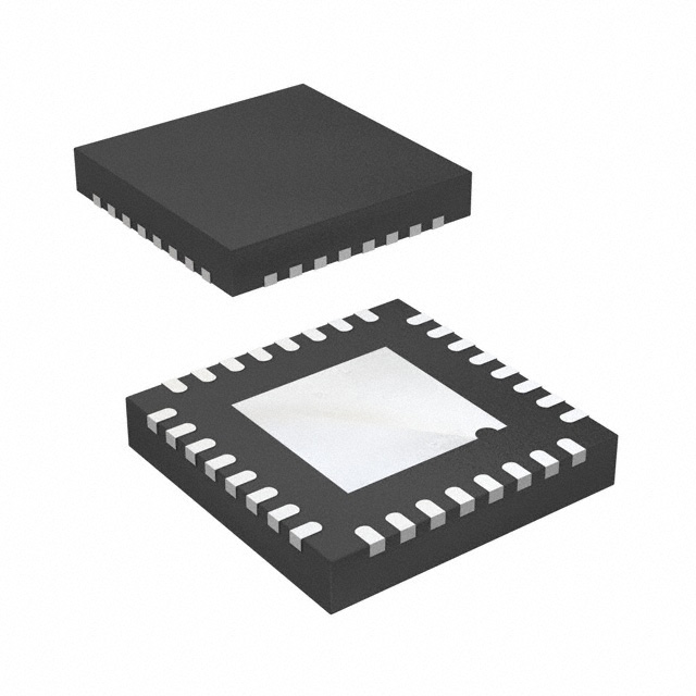
Datasheet
4.5V to 28V, 4A 1ch
Synchronous Buck Converter Integrated FET
BD95514MUV
General Description
BD95514MUV is a switching regulator with current capability of 4A and the ability to achieve low output voltages of 0.7V to
5.0V from a wide input voltage range of 4.5V to 28V. Built-in NMOS power transistors and implementation of Simple Light
Load Mode (SLLMTM) technology make this device highly-efficient. SLLMTM improves efficiency when the device is used is
used with light load, providing high efficiency over a wider range of loads. The device also uses a new technology called
H3RegTM proprietary control method to achieve ultra-fast transient response against load changes. BD95514MUV is
especially designed for various applications and is integrated with protection features such as soft-start, variable frequency,
short circuit protection with timer latch, over voltage protection, and power good function.
Key Specifications
Features
Internal 5V Linear Voltage Regulator (100mA)
Integrated H3RegTM DC/DC Converter Controller
Selectable Simple Light Load Mode (SLLMTM), Quiet
Light Load Mode (QLLM) and Forced Continuous Mode
Built-in Thermal Shutdown, Low Input, Current
Overload, Output Over/Under-Voltage Protection
Circuitry
Soft Start Function to Minimize Rush Current during
Startup
Adjustable Switching Frequency (f = 200kHz to
1000kHz:It changes depending on the setup
condition.)
Built-in Output Discharge Function
Tracking Function
Internal Bootstrap Diode
Input Voltage Range:
Output Voltage Range:
Output Current:
High Side ON-Resistance:
Low Side ON-Resistance:
Standby Current:
Operating Temperature Range:
Package
4.5V to 28V
0.7V to 5.0V
4.0A(Max)
120mΩ(Typ)
120mΩ(Typ)
0μA (Typ)
-10°C to +100°C
W (Typ) x D (Typ) x H (Max)
Application
VQFN032V5050
5.00mm x 5.00mm x 1.00mm
Mobile PCs, desktop PCs, LCD-TV, Digital Household
Electronics
VOUT
Typical Application Circuit
L1
VOUT
D1
C14
GND_VIN
R4
R22
VDD
D
PGN
SW
SW
SW
SW
SW
C8
D
SW
VIN
PGN
VIN
C9
VIN
PGND
C10
VIN
PGND
C11
VIN
PGND
VIN
VDD
R9
BOOT
C12
PGOOD
SW3
REF
REF
SS
C
VREG
EXTVC
VCC
GND
FS
EN
D CTL
MODE
R7
FB
MODE
VDD C7
C13
VOUT
AVIN
CTL
GND_VDD
CE
PGOOD
SW1
GND_VOUT
R8
C6
VDD
C19
VDD
R6
R5
VDD
SW2
R17
C1
EN
C2
R2 C4 C5
SS
VCC
R1
VREG R18
GN
PGND
D
GN
D
Figure 1. Typical Application Circuit
○Product structure:Silicon monolithic integrated circuit
.www.rohm.com
© 2014 ROHM Co., Ltd. All rights reserved.
TSZ22111・14・001
VCC
EXTVCC
○This product has no designed protection against radioactive rays
1/23
TSZ02201-0A1A0A900070-1-2
27.Nov.2014 Rev.001
�BD95514MUV
Pin Configuration
(TOP VIEW)
PGND
24
PGND PGND
23
22
VDD
CE
VOUT
FB
REF
21
20
19
18
17
16 SS
PGND 25
SW 26
15 VREG
SW 27
14 EXTVCC
SW 28
13 VCC
SW 29
12 GND
SW 30
11 FS
SW 31
10 EN
PGND 32
9
1
2
3
4
VIN
VIN
VIN
VIN
5
6
7
BOOT PGOOD AVIN
MODE
8
CTL
Note: Connect the underside (FIN) to the ground terminal
Figure 2. Pin Configuration
Pin Description
(Function Table)
Pin No.
Pin Name
Pin Function
Battery voltage input (4.5V to 28 V)
1 to 4
VIN
5
BOOT
6
PGOOD
7
AVIN
Battery voltage sense
8
CTL
9
MODE
10
EN
Linear regulator ON/OFF (high = 5.0V, low = OFF)
Control mode selection
GND
:Continuous Mode
3.0V
: QLLM
VCC : SLLMTM
Enable output (high when VOUT ON)
11
FS
Switching frequency adjustment (RFS = 30kΩ to 300kΩ)
12
GND
Sense ground
13
VCC
Power supply input
14
EXTVCC
15
VREG
16
SS
17
REF
18
FB
19
VOUT
20
CE
21
VDD
22 to 25
PGND
26 to 31
SW
32
PGND
Underside
FIN
www.rohm.com
© 2014 ROHM Co., Ltd. All rights reserved.
TSZ22111・15・001
HG driver power supply
Power good output (high when output ±10% of regulation)
External power supply input
IC reference voltage (5.0V / 100mA)
Soft start condenser input
Output reference voltage (0.7V)
Feedback input (0.7V)
Voltage discharge output
Reversing HG output
Power supply input (5V)
Power ground
Output to inductor
Power ground
Substrate connection
2/23
TSZ02201-0A1A0A900070-1-2
27.Nov.2014 Rev.001
�BD95514MUV
Block Diagram
VCC
AVIN
13
SS
16
7
VDD
EN
BOOT
5
10
VREG
AVIN
Reference
Block
UVLO
Soft Start
VIN
1
SS
2
8
3
CTL
OVP
VREF x 0.85
VSS x 0.85
VOUT
REF(0.7V)
PGOOD
OCP
SW
SCP
HG
Delay
26
27
17
6
4
ILIM
MODE
EN
Power
Good
H3RegTM
Controller
Block
R
MODE
Q
28
29
MODE
SS
Driver
Circuit
30
S
31
FB
21
18
VDD
LG
AVIN
EXTVCC
14
UVLO
ILIM
SCP
TSD
REF x 1.2
22
FB
PGND
OVP
23
24
Thermal
Protection
25
TSD
32
20
5V Reg
CE
19
EN/UVLO
MODE
15
9
11
VREG
FS
VOUT
12
MODE
GND
Figure 3. Block Diagram
Description of Blocks
1. VCC (Pin 13)
This is the power supply pin for the IC’s internal circuits, except for the FET driver. The input supply voltage ranges from
4.5V to 5.5 V. This pin should be bypassed with either a power capacitor or RC filter.
2. EN (Pin 10)
Enables or disables the switching regulator. When the voltage on this pin reaches 2.3V or higher, the internal switching
regulator is turned ON. At voltages less than 0.8V, the regulator is turned OFF.
3. VDD (Pin 21)
This pin supplies power to the low side of the FET driver, as well as to the bootstrap diode. As the diode draws its peak
current when switching on or off, this pin should be bypassed with a capacitance of approximately 1µF.
4. VREG (Pin 15)
Output pin of the 5V linear regulator. This pin also supplies power to the internal driver and control circuitry. VREG standby
function is controlled by the CTL pin. The output supplies 5V at 100mA and should be bypassed to ground using a 10 µF
capacitor with a rating of X5R or X7R.
5. EXTVCC (Pin 14)
External power supply input for the linear regulator. When the voltage on the EXTVCC pin exceeds 4.4V, the regulator uses
it in conjunction with other power sources to supply VREG. Connect the EXTVCC pin to GND when not in use.
6. REF (Pin 14)
Reference voltage output pin. The reference voltage is set internally by the IC to 0.7V, and the IC works to keep V REF
approximately equal to VFB. Variations in voltage level on this pin affect the output voltage, so the pin should be bypassed
with a 100pF to 0.1µF ceramic capacitor.
www.rohm.com
© 2014 ROHM Co., Ltd. All rights reserved.
TSZ22111・15・001
3/23
TSZ02201-0A1A0A900070-1-2
27.Nov.2014 Rev.001
�BD95514MUV
Description of Blocks – continued
7. SS (Pin 16)
Soft start pin. When EN is set to high, the capacitor between the internal current source (typ:2.2μA) and SS-GND controls
the startup time of the IC. When the voltage on the SS pin is lower than the REF output voltage (0.7V), the output voltage is
held at the same voltage as the SS pin.
8. AVIN (Pin 7)
The BD95514MUV controls the duty cycle and output voltage based on the input voltage at this pin, so voltage variations or
oscillations on this line can cause unstable operation. This pin also acts as the voltage input for the switching block, so
insufficient coupling impedance can also cause unstable operation. Therefore, this line should be bypassed with either a
power capacitor or RC filter.
9. FS (Pin 11)
Frequency-adjusting resistance input pin. Attaching a resistance of 30kΩ to 300kΩ adjusts the switching frequency from
200 kHz to 1MHz (p.11).
10. BOOT (Pin 5)
This pin serves as the power source for the high side of the FET driver. A bootstrap diode is integrated within the IC. The
maximum voltage on this pin should not exceed +30V with reference to GND or +7V with reference to SW. When operating
the switching regulator, the operation of the bootstrap circuitry causes the BOOT voltage to swing from (VIN + VDD) to VDD.
11. PGOOD (Pin 6)
Power good indicator. This open-drain output should be connected to a power supply via a 100kΩ pull-up resistor.
12. MODE (Pin 9)
Mode selection pin. When low, the IC functions in forced-continuous mode; at voltages 0V Pin B, the P-N junction operates as a parasitic diode.
When GND > Pin B, the P-N junction operates as a parasitic transistor.
Parasitic diodes inevitably occur in the structure of the IC. The operation of parasitic diodes can result in mutual
interference among circuits, operational faults, or physical damage. Therefore, conditions that cause these diodes to
operate, such as applying a voltage lower than the GND voltage to an input pin (and thus to the P substrate) should
be avoided.
Resistor
Transistor (NPN)
Pin A
Pin B
C
E
Pin A
N
P+
P
N
N
P+
N
Pin B
B
Parasitic
Elements
N
P+
N P
N
P+
B
N
C
E
Parasitic
Elements
P Substrate
P Substrate
GND
GND
Parasitic
Elements
GND
Parasitic
Elements
GND
N Region
close-by
Figure 17. Example of monolithic IC structure
13. Area of Safe Operation (ASO)
Operate the IC such that the output voltage, output current, and power dissipation are all within the Area of Safe
Operation (ASO).
14. Thermal Shutdown Circuit(TSD)
This IC has a built-in thermal shutdown circuit that prevents heat damage to the IC. Normal operation should always
be within the IC’s power dissipation rating. If however the rating is exceeded for a continued period, the junction
temperature (Tj) will rise which will activate the TSD circuit that will turn OFF all output pins. When the Tj falls below
the TSD threshold, the circuits are automatically restored to normal operation.
Note that the TSD circuit operates in a situation that exceeds the absolute maximum ratings and therefore, under no
circumstances, should the TSD circuit be used in a set design or for any purpose other than protecting the IC from
heat damage.
BD95514MUV
TSD ON Temp. [°C] (typ)
Hysteresis Temp. [°C] (typ)
175
15
15. Ground wiring traces
When using both small-signal and large-current GND traces, the two ground traces should be routed separately but
connected to a single ground potential within the application in order to avoid variations in the small-signal ground
caused by large currents. Also ensure that the GND traces of external components do not cause variations on GND
voltage.
www.rohm.com
© 2014 ROHM Co., Ltd. All rights reserved.
TSZ22111・15・001
20/23
TSZ02201-0A1A0A900070-1-2
27.Nov.2014 Rev.001
�BD95514MUV
Ordering Information
B
D
9
5
5
1
Part Number
4
M
U
V
-
Package
MUV: VQFN032V5050
E2
Packaging and forming specification
E2: Embossed tape and reel
Marking Diagram
VQFN032V5050 (TOP VIEW)
Part Number Marking
D95514
LOT Number
1PIN MARK
www.rohm.com
© 2014 ROHM Co., Ltd. All rights reserved.
TSZ22111・15・001
21/23
TSZ02201-0A1A0A900070-1-2
27.Nov.2014 Rev.001
�BD95514MUV
Physical Dimension, Tape and Reel information
Package Name
www.rohm.com
© 2014 ROHM Co., Ltd. All rights reserved.
TSZ22111・15・001
VQFN032V5050
22/23
TSZ02201-0A1A0A900070-1-2
27.Nov.2014 Rev.001
�BD95514MUV
Revision History
Date
Revision
27.Nov.2014
001
Changes
New Release
www.rohm.com
© 2014 ROHM Co., Ltd. All rights reserved.
TSZ22111・15・001
23/23
TSZ02201-0A1A0A900070-1-2
27.Nov.2014 Rev.001
�Notice
Precaution on using ROHM Products
1.
Our Products are designed and manufactured for application in ordinary electronic equipments (such as AV equipment,
OA equipment, telecommunication equipment, home electronic appliances, amusement equipment, etc.). If you
(Note 1)
intend to use our Products in devices requiring extremely high reliability (such as medical equipment
, transport
equipment, traffic equipment, aircraft/spacecraft, nuclear power controllers, fuel controllers, car equipment including car
accessories, safety devices, etc.) and whose malfunction or failure may cause loss of human life, bodily injury or
serious damage to property (“Specific Applications”), please consult with the ROHM sales representative in advance.
Unless otherwise agreed in writing by ROHM in advance, ROHM shall not be in any way responsible or liable for any
damages, expenses or losses incurred by you or third parties arising from the use of any ROHM’s Products for Specific
Applications.
(Note1) Medical Equipment Classification of the Specific Applications
JAPAN
USA
EU
CHINA
CLASSⅢ
CLASSⅡb
CLASSⅢ
CLASSⅢ
CLASSⅣ
CLASSⅢ
2.
ROHM designs and manufactures its Products subject to strict quality control system. However, semiconductor
products can fail or malfunction at a certain rate. Please be sure to implement, at your own responsibilities, adequate
safety measures including but not limited to fail-safe design against the physical injury, damage to any property, which
a failure or malfunction of our Products may cause. The following are examples of safety measures:
[a] Installation of protection circuits or other protective devices to improve system safety
[b] Installation of redundant circuits to reduce the impact of single or multiple circuit failure
3.
Our Products are designed and manufactured for use under standard conditions and not under any special or
extraordinary environments or conditions, as exemplified below. Accordingly, ROHM shall not be in any way
responsible or liable for any damages, expenses or losses arising from the use of any ROHM’s Products under any
special or extraordinary environments or conditions. If you intend to use our Products under any special or
extraordinary environments or conditions (as exemplified below), your independent verification and confirmation of
product performance, reliability, etc, prior to use, must be necessary:
[a] Use of our Products in any types of liquid, including water, oils, chemicals, and organic solvents
[b] Use of our Products outdoors or in places where the Products are exposed to direct sunlight or dust
[c] Use of our Products in places where the Products are exposed to sea wind or corrosive gases, including Cl2,
H2S, NH3, SO2, and NO2
[d] Use of our Products in places where the Products are exposed to static electricity or electromagnetic waves
[e] Use of our Products in proximity to heat-producing components, plastic cords, or other flammable items
[f] Sealing or coating our Products with resin or other coating materials
[g] Use of our Products without cleaning residue of flux (even if you use no-clean type fluxes, cleaning residue of
flux is recommended); or Washing our Products by using water or water-soluble cleaning agents for cleaning
residue after soldering
[h] Use of the Products in places subject to dew condensation
4.
The Products are not subject to radiation-proof design.
5.
Please verify and confirm characteristics of the final or mounted products in using the Products.
6.
In particular, if a transient load (a large amount of load applied in a short period of time, such as pulse. is applied,
confirmation of performance characteristics after on-board mounting is strongly recommended. Avoid applying power
exceeding normal rated power; exceeding the power rating under steady-state loading condition may negatively affect
product performance and reliability.
7.
De-rate Power Dissipation (Pd) depending on Ambient temperature (Ta). When used in sealed area, confirm the actual
ambient temperature.
8.
Confirm that operation temperature is within the specified range described in the product specification.
9.
ROHM shall not be in any way responsible or liable for failure induced under deviant condition from what is defined in
this document.
Precaution for Mounting / Circuit board design
1.
When a highly active halogenous (chlorine, bromine, etc.) flux is used, the residue of flux may negatively affect product
performance and reliability.
2.
In principle, the reflow soldering method must be used on a surface-mount products, the flow soldering method must
be used on a through hole mount products. If the flow soldering method is preferred on a surface-mount products,
please consult with the ROHM representative in advance.
For details, please refer to ROHM Mounting specification
Notice-GE
© 2013 ROHM Co., Ltd. All rights reserved.
Rev.003
�Precautions Regarding Application Examples and External Circuits
1.
If change is made to the constant of an external circuit, please allow a sufficient margin considering variations of the
characteristics of the Products and external components, including transient characteristics, as well as static
characteristics.
2.
You agree that application notes, reference designs, and associated data and information contained in this document
are presented only as guidance for Products use. Therefore, in case you use such information, you are solely
responsible for it and you must exercise your own independent verification and judgment in the use of such information
contained in this document. ROHM shall not be in any way responsible or liable for any damages, expenses or losses
incurred by you or third parties arising from the use of such information.
Precaution for Electrostatic
This Product is electrostatic sensitive product, which may be damaged due to electrostatic discharge. Please take proper
caution in your manufacturing process and storage so that voltage exceeding the Products maximum rating will not be
applied to Products. Please take special care under dry condition (e.g. Grounding of human body / equipment / solder iron,
isolation from charged objects, setting of Ionizer, friction prevention and temperature / humidity control).
Precaution for Storage / Transportation
1.
Product performance and soldered connections may deteriorate if the Products are stored in the places where:
[a] the Products are exposed to sea winds or corrosive gases, including Cl2, H2S, NH3, SO2, and NO2
[b] the temperature or humidity exceeds those recommended by ROHM
[c] the Products are exposed to direct sunshine or condensation
[d] the Products are exposed to high Electrostatic
2.
Even under ROHM recommended storage condition, solderability of products out of recommended storage time period
may be degraded. It is strongly recommended to confirm solderability before using Products of which storage time is
exceeding the recommended storage time period.
3.
Store / transport cartons in the correct direction, which is indicated on a carton with a symbol. Otherwise bent leads
may occur due to excessive stress applied when dropping of a carton.
4.
Use Products within the specified time after opening a humidity barrier bag. Baking is required before using Products of
which storage time is exceeding the recommended storage time period.
Precaution for Product Label
QR code printed on ROHM Products label is for ROHM’s internal use only.
Precaution for Disposition
When disposing Products please dispose them properly using an authorized industry waste company.
Precaution for Foreign Exchange and Foreign Trade act
Since our Products might fall under controlled goods prescribed by the applicable foreign exchange and foreign trade act,
please consult with ROHM representative in case of export.
Precaution Regarding Intellectual Property Rights
1.
All information and data including but not limited to application example contained in this document is for reference
only. ROHM does not warrant that foregoing information or data will not infringe any intellectual property rights or any
other rights of any third party regarding such information or data. ROHM shall not be in any way responsible or liable
for infringement of any intellectual property rights or other damages arising from use of such information or data.:
2.
No license, expressly or implied, is granted hereby under any intellectual property rights or other rights of ROHM or any
third parties with respect to the information contained in this document.
Other Precaution
1.
This document may not be reprinted or reproduced, in whole or in part, without prior written consent of ROHM.
2.
The Products may not be disassembled, converted, modified, reproduced or otherwise changed without prior written
consent of ROHM.
3.
In no event shall you use in any way whatsoever the Products and the related technical information contained in the
Products or this document for any military purposes, including but not limited to, the development of mass-destruction
weapons.
4.
The proper names of companies or products described in this document are trademarks or registered trademarks of
ROHM, its affiliated companies or third parties.
Notice-GE
© 2013 ROHM Co., Ltd. All rights reserved.
Rev.003
�Datasheet
General Precaution
1. Before you use our Pro ducts, you are requested to care fully read this document and fully understand its contents.
ROHM shall n ot be in an y way responsible or liabl e for fa ilure, malfunction or acci dent arising from the use of a ny
ROHM’s Products against warning, caution or note contained in this document.
2. All information contained in this docume nt is current as of the issuing date and subj ect to change without any prior
notice. Before purchasing or using ROHM’s Products, please confirm the la test information with a ROHM sale s
representative.
3.
The information contained in this doc ument is provi ded on an “as is” basis and ROHM does not warrant that all
information contained in this document is accurate an d/or error-free. ROHM shall not be in an y way responsible or
liable for an y damages, expenses or losses incurred b y you or third parties resulting from inaccur acy or errors of or
concerning such information.
Notice – WE
© 2014 ROHM Co., Ltd. All rights reserved.
Rev.001
�