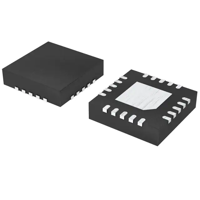
Datasheet
2 Cell / 3 Cell Narrow VDC Charger with
SMBus Interface
BD99950MUV
General Description
Key Specifications
The BD99950MUV is a high-efficiency, synchronous
Narrow VDC system voltage regulator and battery
charger controller. It has two charge pumps which
separately drive N-channel MOSFETs for automatic
system power source selection. Charge voltage, charge
current, AC adapter current and minimum system
voltage can be programmed through SMBus. With a
small inductor, PWM switching frequency can also be
programmed by SMBus up to 1.2MHz.
Structure
Silicon Monolithic Integrated Circuit
Features
Input Voltage Range:
6.0V to 24.0V
Output Voltage Range:
3.072V to 16.384V
Charge Voltage Accuracy:
±0.5%
Switching Frequency:
600kHz to 1.2MHz
Battery Standby Current:
17μA (Typ)
Operating Temperature Range: -10°C to +85°C
Package
N-channel MOSFETs available for Battery or
Adapter Selection via Internal Charge Pumps
Fast DPM Transient Response under Turbo
Mode( 5.0V
2.4V < ACDET Voltage < 3.15V
VCC Voltage – SRN Voltage > 300mV
After the first IC power on reset, the ACOK rising edge delay is always 1.3s. Set the Charge Option() bit[15] to 0 to
set the rise deglitch time to 150ms.
When the ACDET pin voltage is higher than 3.15V, it is considered as AC adapter over voltage. ACOK will be pulled
low, and charging will be disabled. The ACGATE Charge Pump will be turned off to disconnect the high voltage AC
adapter during ACOVP.
When ACDET pin voltage falls below 3.15V and above 2.4V, it is considered as the adapter voltage returning back to
its normal voltage. ACOK will be pulled high by an external pull up resistor.
○ Transition from Trickle Charge mode to Fast Charge mode
Transition from trickle charge to CC charge (fast charge mode) occurs by detecting the decrease in trickle charge
current. When the trickle charge current drops to less than 100mA from its set value, it automatically switches to CC
charge (fast charge). To enable the transition to fast charge, the charge current must be set to more than 256mA.
www.rohm.com
© 2019 ROHM Co., Ltd. All rights reserved.
TSZ22111 • 15 • 001
16/34
TSZ02201-0J1J0A700570-1-2
25.Jan.2019.Rev.005
�BD99950MUV
○ Charge OCP
When the charging current exceeds 100mA more than the set charge current, the DAC and charger restart to protect
the battery from over current.
○ Over Charge Voltage Setting Protection
When a write to the Charge Voltage() register is detected during CV charging mode, charging resets to protect
battery from over-current.
○ Setting Charge Options
The charge options are set by writing a valid 16-bit number to the charge option register. Each bit in the control
register has a different function. Table 3 describes the function of each bit. Bits 2 and 4 are controlled internally and are
read only.
Table 3. Charge Options Register (0x12H)
BIT
[15]
[14:13]
BIT NAME
ACOK Deglitch Time Setting
Watchdog Timer Setting
[12]
SLLM mode
[11]
BGATE Charge Pump Enable
[10:9]
[8]
[7]
Switching Frequency setting
High Side FET OCP
Comparator Threshold Setting
Low Side FET OCP
Comparator Threshold Setting
[6]
LEARN Enable
[5]
IOUT Selection
[4]
ACOK Indication
(Read Only)
[3]
Charge Over Current
Protection
[2]
Trickle Charge Indication
(Read Only)
[1]
ACOC Enable
[0]
Shut down
www.rohm.com
© 2019 ROHM Co., Ltd. All rights reserved.
TSZ22111 • 15 • 001
DESCRIPTION
0: ACOK rising edge deglitch time 150ms
1: ACOK rising edge deglitch time 1.3s
00: Disable Watchdog Timer
01: Enabled, 44 sec
10: Enabled, 88 sec
11: Enable Watchdog Timer (175s)
0: Fixed Frequency Switching
1: Variable Frequency Switching(SLLM mode)
0: BGATE Charge Pump ON
1: BGATE Charge Pump OFF(from HOST when battery is removed)
00: 600kHz
01: 800kHz
10: 1MHz
11: 1.2MHz
0: function is disabled
1: 450mV
0: 135mV
1: 230mV
0: Disable LEARN Cycle
1: Enable LEARN Cycle
0: IOUT is the 20x Adapter Current Amplifier Output
1: IOUT is the 20x Charge Current Amplifier Output
Adapter Detection Indicator
0: AC adapter is not present (ACDET < 2.4V)
1: AC adapter is present (ACDET > 2.4V)
0: Charge Current DAC Reset and Charger Restart
1: Charge Current DAC Reset
Trickle Charge Indicator
0: Charge in Switching Mode
1: In Trickle Charge mode(Linear charge mode )
0: ACOC Disable
1: 3.33x of Adapter Current Setting
0: Enable NVDC Charger Control
1: Shut Down
17/34
TSZ02201-0J1J0A700570-1-2
25.Jan.2019.Rev.005
�BD99950MUV
○ Setting the Charge Voltage
The charge voltage is set by writing a valid 16-bit number to the Charge Voltage register. The first 4 LSBs are
ignored and the next 11 bits are used to set the charge voltage through a DAC. The charge voltage range of the
BD99950MUV is 3.072V to 16.384V. The register address for charge voltage is 0x15. The 16-bit binary number formed
by D15-D0 represents the charge voltage set point in mV. However, the resolution becomes 16mV because the D0-D3
bits are ignored. The D15 bit is also ignored because it is not needed to span the 3.072V to 16.384V range.
Table 4. Charge Voltage Register (0x15H)
BIT
BIT NAME
0
-
Not used
1
-
Not used
2
-
Not used
3
-
Not used
4
Charge Voltage, DACV 0
5
Charge Voltage, DACV 1
6
Charge Voltage, DACV 2
7
Charge Voltage, DACV 3
8
Charge Voltage, DACV 4
9
Charge Voltage, DACV 5
10
Charge Voltage, DACV 6
11
Charge Voltage, DACV 7
12
Charge Voltage, DACV 8
13
Charge Voltage, DACV 9
14
Charge Voltage, DACV 10
15
-
www.rohm.com
© 2019 ROHM Co., Ltd. All rights reserved.
TSZ22111 • 15 • 001
DESCRIPTION
0 = Adds 0mV of charger voltage, 1024mV min
1 = Adds 16mV of charger voltage
0 = Adds 0mV of charger voltage, 1024mV min
1 = Adds 32mV of charger voltage
0 = Adds 0mV of charger voltage, 1024mV min
1 = Adds 64mV of charger voltage
0 = Adds 0mV of charger voltage, 1024mV min
1 = Adds 128mV of charger voltage
0 = Adds 0mV of charger voltage, 1024mV min
1 = Adds 256mV of charger voltage
0 = Adds 0mV of charger voltage, 1024mV min
1 = Adds 512mV of charger voltage
0 = Adds 0mA of charger voltage
1 = Adds 1024mV of charger voltage
0 = Adds 0mV of charger voltage
1 = Adds 2048mV of charger voltage
0 = Adds 0mV of charger voltage
1 = Adds 4096mV of charger voltage
0 = Adds 0mV of charger voltage
1 = Adds 8192mV of charger voltage
0 = Adds 0mV of charger voltage
1 = Adds 16384mV of charger voltage, 16384mV max
Not used.
18/34
TSZ02201-0J1J0A700570-1-2
25.Jan.2019.Rev.005
�BD99950MUV
○ Setting the Charge Current
The charge current is set by writing a valid 16-bit number to the Charge Current register. The first 6 LSBs are
ignored and the next 7 bits are used to set the charge current through a DAC. The charge current range of the
BD99950MUV is 128mA to 8.128A. The register address for charge current is 0x14. The 16-bit binary number formed
by D15-D0 represents the charge current set point in mA. However, the resolution becomes 64mA because the D0-D5
bits are ignored. The D13-D15 bits are also ignored because they are not needed to span the 128mA to 8.128A range.
To change “Trickle Charge” to “Fast Charge”, a setting of 256mA or higher is required.
Table 5. Charge Current Register (0x14H), Using 10mΩ Sense Resistor
BIT
BIT NAME
0
-
Not used
1
-
Not used
2
-
Not used
3
-
Not used
4
-
Not used
5
-
Not used
6
Charge Current, DACI 0
7
Charge Current, DACI 1
8
Charge Current, DACI 2
9
Charge Current, DACI 3
10
Charge Current, DACI 4
11
Charge Current, DACI 5
12
Charge Current, DACI 6
DESCRIPTION
0 = Adds 0mA of charger current
1 = Adds 64mA of charger current
0 = Adds 0mA of charger current
1 = Adds 128mA of charger current
0 = Adds 0mA of charger current
1 = Adds 256mA of charger current
0 = Adds 0mA of charger current
1 = Adds 512mA of charger current
0 = Adds 0mA of charger current
1 = Adds 1024mA of charger current
0 = Adds 0mA of charger current
1 = Adds 2048mA of charger current
0 = Adds 0mA of charger current
1 = Adds 4096mA of charger current, 8128mA max
13
-
Not used
14
-
Not used
15
-
Not used
www.rohm.com
© 2019 ROHM Co., Ltd. All rights reserved.
TSZ22111 • 15 • 001
19/34
TSZ02201-0J1J0A700570-1-2
25.Jan.2019.Rev.005
�BD99950MUV
○ Setting the Input Current
The input current is set by writing a valid 16-bit number to the Input Current register. The first 7 LSBs are ignored and
the next 7 bits are used to set the input current through a DAC. The input current range of the BD99950MUV is 512mA
to 6.144A. The register address for input Current is 0x3F. The 16-bit binary number formed by D15-D0 represents the
input current set point in mA. However, the resolution becomes 64mA because the D0-D5 bits are ignored. The
D13-D15 bits are also ignored because they are not needed to span the 512mA to 6.144A range. To set for more than
6.144A the sense resistor must be changed to 10mΩ.
Table 6. Input Current Register (0x3FH), Using 20mΩ Sense Resistor
BIT
BIT NAME
0
-
Not used
1
-
Not used
2
-
Not used
3
-
Not used
4
-
Not used
5
-
Not used
6
Charge Current, DACS 0
7
Charge Current, DACS 1
8
Charge Current, DACS 2
9
Charge Current, DACS 3
10
Charge Current, DACS 4
11
Charge Current, DACS 5
12
Charge Current, DACS 6
DESCRIPTION
0 = Adds 0mA of input current
1 = Adds 64mA of input current
0 = Adds 0mA of input r current
1 = Adds 128mA of input current
0 = Adds 0mA of input current
1 = Adds 256mA of input current
0 = Adds 0mA of input current
1 = Adds 512mA of input current
0 = Adds 0mA of input current
1 = Adds 1024mA of input current
0 = Adds 0mA of input current
1 = Adds 2048mA of input current
0 = Adds 0mA of input current
1 = Adds 4096mA of input current, 6144mA max
13
-
Not used
14
-
Not used
15
-
Not used
www.rohm.com
© 2019 ROHM Co., Ltd. All rights reserved.
TSZ22111 • 15 • 001
20/34
TSZ02201-0J1J0A700570-1-2
25.Jan.2019.Rev.005
�BD99950MUV
○ Setting the Minimum System Voltage
The minimum system voltage is set by writing a valid 16-bit number to the Minimum System Voltage register. The
first 6 LSBs are ignored and the next 8 bits are used to set the minimum system voltage through a DAC. The minimum
system voltage range of the BD99950MUV is 3.072V to 10.24V. The register address for Minimum System Voltage is
0x3E. The 16-bit binary number formed by D15-D0 represents the minimum system voltage set point in mV. However,
the resolution becomes 64mV because the D0-D5 bits are ignored. The D14-D15 bits are also ignored because they
are not needed to span the 3.072V to 10.24V range.
Table 7. Minimum System Voltage Register (0x3EH)
BIT
BIT NAME
0
-
Not used
1
-
Not used
2
-
Not used
3
-
Not used
4
-
Not used
5
-
Not used
6
Charge Current, DACV 0
7
Charge Current, DACV 1
8
Charge Current, DACV 2
9
Charge Current, DACV 3
10
Charge Current, DACV 4
11
Charge Current, DACV 5
12
Charge Current, DACV 6
13
Charge Current, DACV 7
DESCRIPTION
0 = Adds 0mV of minimum system voltage, 1024mV min
1 = Adds 64mV of minimum system voltage
0 = Adds 0mV of minimum system voltage, 1024mV min
1 = Adds 128mV of minimum system voltage
0 = Adds 0mV of minimum system voltage, 1024mV min
1 = Adds 256mV of minimum system voltage
0 = Adds 0mV of minimum system voltage, 1024mV min
1 = Adds 512mV of minimum system voltage
0 = Adds 0mA of minimum system voltage
1 = Adds 1024mV of minimum system voltage
0 = Adds 0mV of minimum system voltage
1 = Adds 2048mV of minimum system voltage
0 = Adds 0mV of minimum system voltage
1 = Adds 4096mV of minimum system voltage
0 = Adds 0mV of minimum system voltage
1 = Adds 8192mV of minimum system voltage, 10240mV max
14
-
Not used
15
-
Not used
www.rohm.com
© 2019 ROHM Co., Ltd. All rights reserved.
TSZ22111 • 15 • 001
21/34
TSZ02201-0J1J0A700570-1-2
25.Jan.2019.Rev.005
�BD99950MUV
External Components Selection
○ Inductor and Output Capacitor
Low ESR MLCC needs to be used to reduce ripple voltage. The inductance also has a great influence on ripple
current which flows in the inductor. Ripple current that flows in inductor can be calculated using Formula (1).
As shown in Formula (1), the bigger the coil is or the higher the switching frequency is, less ripple current flows.
ΔI L =
(Vcc - VOUT) × VOUT
[A] (1)
L × Vcc × f
Ripple current must be 30-50% of the maximum output current.
ΔI L = 0.3 - 0.5 × IOUTMAX
[A]
L=
(Vcc - VOUT) × VOUT
[H]
ΔI × Vcc × f
L
( ΔI
L : output ripple current
IL
ΔIL
f : sw itchingfrequency)
※Peak current must be set lower than the maximum current of the inductor. (Refer to inductor specification)
※In order to improve efficiency, lower DCR/ACR inductor is recommended.
※The increase of output ripple voltage may lower the charge current detection accuracy.
19V Adapter 2cell battery (fsw = 800kHz)
Adapter Capability
10W
20W
30W
40W
Max output Current
1.7A
3.4A
5.1A
6.8A
Inductor(μH)
4.7
3.3
3.3 or 2.2
2.2
Output Capacitor(μF)
SRP-SRN
Sense Resistor(mΩ)
22
33
44
44
10
10
10
10
○ ACDET Resistor
An attenuated value of the AC adapter voltage is inputted to the ACDET pin using a voltage divider. Set the ACDET
voltage so that the range is 2.4V to 3.15V when the AC adapter is inputted.
To lower the response speed of UVP and OVP due to noise in the AC adapter, insert capacitor C16 parallel to
resistor R7 for filtering.
Example of setting
AC Adapter Voltage
10.5V
12V
15V
16V
19V
20V
24V
Battery
2cell
2cell
2cell/3cell
2cell/3cell
2cell/3cell
2cell/3cell
2cell/3cell
R6(Ω)
150k
180k
180k
200k
240k
240k
270k
R7(Ω)
ACOK Voltage
Rising Edge (typical)
ACOVP Voltage
Rising Edge (typical)
51k
51k
39k
39k
39k
36k
33k
9.5V
10.9V
13.5V
14.7V
17.2V
18.4V
22.0V
12.4V
14.3V
17.7V
19.3V
22.5V
24.2V
29.0V
○ Reverse Input Protection Circuit
A protection circuit can be inserted (refer to Figure 26) in case the polarity of the AC adapter or the battery is
reversed.
○ Switching Power MOSFET (Q1,Q2)
To decrease switching loss and to improve efficiency, select a FET with a small on-resistance and less gate capacity.
○ AC Adapter and Battery Pass Power MOSFET (Q3,Q4)
To decrease loss during operation, choose a FET with a small on-resistance.
www.rohm.com
© 2019 ROHM Co., Ltd. All rights reserved.
TSZ22111 • 15 • 001
22/34
TSZ02201-0J1J0A700570-1-2
25.Jan.2019.Rev.005
�BD99950MUV
○ VCC Protection Filter when Inserting the AC Adapter
Insert filter with 10Ω/1μF to prevent over-voltage caused by ringing when the AC adapter is inserted. ACP and ACN
terminal are measured by increasing pressure of internal elements.
○ ACN and ACP Differential Mode Noise Filtering
When error is caused on the regulating current due to differential mode noise, insert a
differential mode noise filter with 10Ω/1μF between the ACN and ACP pins.
In this case, do not connect a capacitor between ACN and GND.
20mΩ
10Ω
0.1uF
1uF
ACP
ACN
BD99950MUV
○ SRP, and SRN Capacitor
To prevent inaccuracies in current detection caused by common node noise, place a
0.1μF- 1μF capacitor as close as possible to the analog GND pin.
10mΩ
0Ω
0.1uF
0.1uF
SRP
SRN
BD99950MUV
○ Current Sensing Resistor
During adapter hot plug-in, the parasitic inductance and the input capacitor from the adapter cable form a second
order system. Thus adapter hot plug-in generate over voltage spike. The Voltage spike may be beyond IC Maximum
Voltage and break the IC.
As methods of solving for voltage spike, moving C1 capacitor between R1 and Q3.
Adapter Voltage
Adapter Voltage
Adapter voltage when place C1 capacitor ACP node and hot
Adapter voltage when place input capacitor directry
Plug-in
Adapter node and hot Plug-in
PCB Layout Guideline
○ Current Sensing Resistor
The SRP/ACP and SRN/ACN connection must be laid out as shown in
Figure 25.
Also, connect a 0.1μF capacitor to GND near the pin to decrease common
mode noise.
High Current Line
High Current Line
Current sense Line
Current sense Line
○ LDRV
The LDRV pin is the gate drive terminal of the low-side N-channel MOSFET.
Extremely high charging/discharging slew rate in the gate of the MOSFET can
BD99950MUV
cause a very large current to flow through the REGN, LDRV and GND
terminals. It is therefore advisable to place the gate of the low-side
Figure 25. Current Sense Kelvin Layout
N-channel MOSFET to the LDRV pin as close as possible. Enclosing the
path with a ground shield is also recommended to lessen the unwanted
effects of noise.
SRP
/ ACP
SRN
/ ACN
○ HDRV and PHASE
The HDRV pin is the gate drive terminal of the high-side N-channel MOSFET. Extremely high charging/discharging
slew rate in the gate of the MOSFET can cause a very large current to flow through the BOOT, HDRV and PHASE
terminals. It is therefore advisable to place the gate of the high-side N-channel MOSFET to the HDRV pin as close as
possible. Enclosing the path with a ground shield is also recommended to lessen the unwanted effects of noise.
www.rohm.com
© 2019 ROHM Co., Ltd. All rights reserved.
TSZ22111 • 15 • 001
23/34
TSZ02201-0J1J0A700570-1-2
25.Jan.2019.Rev.005
�BD99950MUV
Figure 26. Reference Design Schematic
Application Example
www.rohm.com
© 2019 ROHM Co., Ltd. All rights reserved.
TSZ22111 • 15 • 001
24/34
TSZ02201-0J1J0A700570-1-2
25.Jan.2019.Rev.005
�BD99950MUV
Input Capacitor C1A (22μF)
Place input capacitor C1A, as close as possible to Q3 drain pin and ground.
Input Capacitor C4 (10μF)
Place input capacitor C4, as close as possible to Q1 drain pin and Q2 source pin.
Select C1A≧ C4 for Fast DPM operation.
Current Sense Resistor R1 (20mΩ), R2 (10mΩ)
Current sense Kelvin layout must be followed. (Refer to “Current Sense Resistance” on page 23.)
Current Sense Pin Capacitor C8, C10, C11 (0.1μF), C17(1μF), C9(Empty) and R11(10Ω)
Place input capacitor C8, C9, C10, C11 as close as possible to their corresponding sense pins.
(Refer to “ACN and ACP Terminal Differential Mode Noise Filtering” on page 23.)
REGN Output Capacitor C7 (1μF)
Place output capacitor C7 as close as possible to REGN pin and to ground.
VCC Decoupling Capacitor C6 (1μF)
Place input decoupling capacitor C6 as close as possible to VCC pin and to ground.
www.rohm.com
© 2019 ROHM Co., Ltd. All rights reserved.
TSZ22111 • 15 • 001
25/34
TSZ02201-0J1J0A700570-1-2
25.Jan.2019.Rev.005
�BD99950MUV
Selection of Components Externally Connected
Reference
Design
Configuration
Value
QTY
Rated
Voltage
Manufacture
Part number
Rohm
HS8K1
X[mm]
Y[mm]
Z[mm]
3.0
3.0
0.8
2.0
2.0
0.8
3.3
3.3
0.8
2.0
2.0
0.8
3.3
3.3
0.8
2.0
2.0
0.8
3.3
3.3
0.8
1.6
1.6
0.5
6.5
7.4
3.0
ALPS
GLMC2R201A
6.6
7.0
3.0
TOKO
FDSD0630-H-2R2M
7.5
7.5
2.0
coilcraft
XAL7020-222ME
1.5uH
4.0
4.0
1.8
coilcraft
KA5013-AE
22uF
2.0
1.25
1.25
1
25V
Murata
GRM21BR61E226ME44#
C2A,C2B
22uF
2.0
1.25
1.25
2
25V
Murata
GRM21BR61E226ME44#
C3
10uF
2.0
1.25
1.25
1
25V
Murata
GRM219BR61E106KA12#
C4
10uF
2.0
1.25
1.25
1
25V
Murata
GRM219BR61E106KA12#
C5
0.1uF
1.0
0.5
0.5
1
16V
Std.
Ceramic Capacitor X5R 10%
C6
1.0uF
1.0
0.5
0.5
1
25V
Murata
GRM155R61E105KA12
C7
1.0uF
1.0
0.5
0.5
1
16V
Std.
Ceramic Capacitor X5R 10%
C8
0.1uF
1.0
0.5
0.5
2
25V
Std.
Ceramic Capacitor X5R 10%
0.1uF
1.0
0.5
0.5
2
25V
Std.
Ceramic Capacitor X5R 10%
C12
0.01uF
1.0
0.5
0.5
1
16V
Std.
Ceramic Capacitor X5R 10%
C13
4700pF
1.0
0.5
0.5
1
6.3V
Std.
Ceramic Capacitor X5R 10%
C14
0.1uF
1.0
0.5
0.5
1
16V
Std.
Ceramic Capacitor X5R 10%
C15(Optional)
100pF
1.0
0.5
0.5
1
16V
Std.
Ceramic Capacitor X5R 10%
C16
0.01uF
1.0
0.5
0.5
1
16V
Std.
Ceramic Capacitor X5R 10%
C17
1.0uF
1.0
0.5
0.5
1
16V
Std.
Ceramic Capacitor X5R 10%
D1
-
1.0
0.6
0.4
1
30V
Rohm
RB520CS-30
R1
20mΩ
2.0
1.2
0.3
1
-
Rohm
UCR10EVHFSR020
R2
10mΩ
2.0
1.2
0.3
1
-
Rohm
PMR10EZPFU10L0
R3(Optional)
R4,R8
(Optional)
R5
5.1kΩ
1.0
0.5
0.35
1
-
Std.
1%
510Ω
1.0
0.5
0.35
2
-
Std.
1%
10Ω
1.0
0.5
0.35
1
-
Std.
1%
R6
240kΩ
1.0
0.5
0.35
1
-
Std.
1%
R7
39kΩ
1.0
0.5
0.35
1
-
Std.
1%
R9(Optional)
1MΩ
1.0
0.5
0.35
1
-
Std.
1%
R10(Optional)
3MΩ
1.0
0.5
0.35
1
-
Std.
1%
R11
10Ω
1.0
0.5
0.35
1
-
Std.
1%
10kΩ
1.0
0.5
0.35
1
-
Std.
1%
2in1
Q1, Q2
Q3
Q4
Q5-1,Q5-2
(Optional)
L
C1A
2in1
2.2uH
1
2
1
30V
30V
1
30V
1
30V
1
-
Rohm
RF4E110GN
Rohm
RQ3E120GN
Rohm
RF4E110GN
Rohm
RQ3E120GN
Rohm
RF4E110GN
Rohm
RQ3E120GN
Rohm
EM6K31
C1B(EMPTY)
C9(Empty)
C10,C11
R40(Empty)
R41(Empty)
R42(Empty)
R43(Empty)
R45
www.rohm.com
© 2019 ROHM Co., Ltd. All rights reserved.
TSZ22111 • 15 • 001
26/34
TSZ02201-0J1J0A700570-1-2
25.Jan.2019.Rev.005
�BD99950MUV
Figure 27. TOP Silk Screen
Figure 28. TOP Copper Trace Layer
(Signal and Ground)
Figure 29. Middle 1 Copper Trace Layer
(Ground)
Figure 30. Middle 2 Copper Trace Layer
(Signal and System Output)
Figure 31. Bottom Copper Trace Layer
(Signal and Ground)
Figure 32. Bottom Silk Screen
www.rohm.com
© 2019 ROHM Co., Ltd. All rights reserved.
TSZ22111 • 15 • 001
27/34
TSZ02201-0J1J0A700570-1-2
25.Jan.2019.Rev.005
�BD99950MUV
Example of Recommended Circuit
Adapter Reverse Input Protection
(optional)
Q5-1
ADAPTER +
Q3
R1
R10
C4
C1A
R11
C12
C17
R9
C8
R3
C9
ACP
ACN
ACGATE
BOOT
VCC
HDRV
C5
R5
R6
Q1
D1
L
C6
ACIN
R7
(
)
Total Csys100μF
LDRV
REGN
C15
SYSTEM
C2A C2B
PHASE
Q2
C7
BD99950MUV
SRP
C10
R2
C11
HOST
SRN
BATTRM
R4
ACOK
Q4
BGATE
SCL
SMBus
C16
SDA
R8
C14
GND
C13
BATTERY+
BATT
IOUT
Q5-2
C3
Battery Reverse Input Protection (optional)
Figure 33. Example of Application Circuit (AC Adapter and Battery Reverse Input Protected Configuration)
Q3
R1
ADAPTER +
C4
C1A
R11
C8
C17
ACP
ACN
BOOT
ACGATE
C5
R5
R6
VCC
Q1
HDRV
D1
L
C6
PHASE
C2A C2B
SYSTEM
ACIN
R7
LDRV
REGN
Q2
C7
BD99950MUV
SRP
C10
HOST
SRN
BATTRM
C11
ACOK
SMBus
Q4
BGATE
R4
SCL
SDA
BATTERY+
BATT
IOUT
C13
R2
C3
GND
Figure 34. Example of Application Circuit (Minimum Component Configuration)
www.rohm.com
© 2019 ROHM Co., Ltd. All rights reserved.
TSZ22111 • 15 • 001
28/34
TSZ02201-0J1J0A700570-1-2
25.Jan.2019.Rev.005
�BD99950MUV
Power Dissipation [W]
Power Dissipation
Measuring instrument : TH-156(KUWANO Electrical Instrument
Condition
: Board mounting
Board dimension
: 114.3mm x 76.2mm x 1.6mmt
2.0
1.5
Four Layer (Surface Copper area 2.25mm2)
(The 2nd and 3rd layer have 5505mm2 copper plane)
(PCB with thermal vias)
θja=61.0℃/W
1.64W
1.0
0.5
0
25
50
75
100 125 150
Ambient Temperature Ta [℃]
Figure 35. Power Dissipation (Solder operated on the PAD backside of 4 layer substrate)
www.rohm.com
© 2019 ROHM Co., Ltd. All rights reserved.
TSZ22111 • 15 • 001
29/34
TSZ02201-0J1J0A700570-1-2
25.Jan.2019.Rev.005
�BD99950MUV
Operational Notes
1.
Reverse Connection of Power Supply
Connecting the power supply in reverse polarity can damage the IC. Take precautions against reverse polarity when
connecting the power supply, such as mounting an external diode between the power supply and the IC’s power
supply pins.
2.
Power Supply Lines
Design the PCB layout pattern to provide low impedance supply lines. Separate the ground and supply lines of the
digital and analog blocks to prevent noise in the ground and supply lines of the digital block from affecting the analog
block. Furthermore, connect a capacitor to ground at all power supply pins. Consider the effect of temperature and
aging on the capacitance value when using electrolytic capacitors.
3.
Ground Voltage
Ensure that no pins are at a voltage below that of the ground pin at any time, even during transient condition. However,
pins that drive inductive loads (e.g. motor driver outputs, DC-DC converter outputs) may inevitably go below ground
due to back EMF or electromotive force. In such cases, the user should make sure that such voltages going below
ground will not cause the IC and the system to malfunction by examining carefully all relevant factors and conditions
such as motor characteristics, supply voltage, operating frequency and PCB wiring to name a few.
4.
Ground Wiring Pattern
When using both small-signal and large-current ground traces, the two ground traces should be routed separately but
connected to a single ground at the reference point of the application board to avoid fluctuations in the small-signal
ground caused by large currents. Also ensure that the ground traces of external components do not cause variations
on the ground voltage. The ground lines must be as short and thick as possible to reduce line impedance.
5.
Thermal Consideration
Should by any chance the power dissipation rating be exceeded the rise in temperature of the chip may result in
deterioration of the properties of the chip. The absolute maximum rating of the Pd stated in this specification is when
the IC is mounted on a 70mm x 70mm x 1.6mm glass epoxy board. In case of exceeding this absolute maximum
rating, increase the board size and copper area to prevent exceeding the Pd rating.
6.
Recommended Operating Conditions
These conditions represent a range within which the expected characteristics of the IC can be approximately obtained.
The electrical characteristics are guaranteed under the conditions of each parameter.
7.
Inrush Current
When power is first supplied to the IC, it is possible that the internal logic may be unstable and inrush
current may flow instantaneously due to the internal powering sequence and delays, especially if the IC
has more than one power supply. Therefore, give special consideration to power coupling capacitance,
power wiring, width of ground wiring, and routing of connections.
8.
Operation Under Strong Electromagnetic Field
Operating the IC in the presence of a strong electromagnetic field may cause the IC to malfunction.
9.
Testing on Application Boards
When testing the IC on an application board, connecting a capacitor directly to a low-impedance output pin may
subject the IC to stress. Always discharge capacitors completely after each process or step. The IC’s power supply
should always be turned off completely before connecting or removing it from the test setup during the inspection
process. To prevent damage from static discharge, ground the IC during assembly and use similar precautions during
transport and storage.
10. Inter-pin Short and Mounting Errors
Ensure that the direction and position are correct when mounting the IC on the PCB. Incorrect mounting may result in
damaging the IC. Avoid nearby pins being shorted to each other especially to ground, power supply and output pin.
Inter-pin shorts could be due to many reasons such as metal particles, water droplets (in very humid environment) and
unintentional solder bridge deposited in between pins during assembly to name a few.
www.rohm.com
© 2019 ROHM Co., Ltd. All rights reserved.
TSZ22111 • 15 • 001
30/34
TSZ02201-0J1J0A700570-1-2
25.Jan.2019.Rev.005
�BD99950MUV
Operational Notes – continued
11. Unused Input Pins
Input pins of an IC are often connected to the gate of a MOS transistor. The gate has extremely high impedance and
extremely low capacitance. If left unconnected, the electric field from the outside can easily charge it. The small
charge acquired in this way is enough to produce a significant effect on the conduction through the transistor and
cause unexpected operation of the IC. So unless otherwise specified, unused input pins should be connected to the
power supply or ground line.
12. Regarding the Input Pin of the IC
This monolithic IC contains P+ isolation and P substrate layers between adjacent elements in order to keep them
isolated. P-N junctions are formed at the intersection of the P layers with the N layers of other elements, creating a
parasitic diode or transistor. For example (refer to figure below):
When GND > Pin A and GND > Pin B, the P-N junction operates as a parasitic diode.
When GND > Pin B, the P-N junction operates as a parasitic transistor.
Parasitic diodes inevitably occur in the structure of the IC. The operation of parasitic diodes can result in mutual
interference among circuits, operational faults, or physical damage. Therefore, conditions that cause these diodes to
operate, such as applying a voltage lower than the GND voltage to an input pin (and thus to the P substrate) should
be avoided.
Resistor
Transistor (NPN)
Pin A
Pin B
C
E
Pin A
N
P+
P
N
N
P+
N
Pin B
B
Parasitic
Elements
N
P+
N P
N
P+
B
N
C
E
Parasitic
Elements
P Substrate
P Substrate
GND
GND
Parasitic
Elements
GND
Parasitic
Elements
GND
N Region
close-by
Figure 36. Example of monolithic IC structure
13. Ceramic Capacitor
When using a ceramic capacitor, determine the dielectric constant considering the change of capacitance with
temperature and the decrease in nominal capacitance due to DC bias and others.
14. Area of Safe Operation (ASO)
Operate the IC such that the output voltage, output current, and power dissipation are all within the Area of Safe
Operation (ASO).
15. Thermal Shutdown Circuit(TSD)
This IC has a built-in thermal shutdown circuit that prevents heat damage to the IC. Normal operation should always
be within the IC’s power dissipation rating. If however the rating is exceeded for a continued period, the junction
temperature (Tj) will rise which will activate the TSD circuit that will turn OFF all output pins. When the Tj falls below
the TSD threshold, the circuits are automatically restored to normal operation.
Note that the TSD circuit operates in a situation that exceeds the absolute maximum ratings and therefore, under no
circumstances, should the TSD circuit be used in a set design or for any purpose other than protecting the IC from
heat damage.
16. Over Current Protection Circuit (OCP)
This IC incorporates an integrated overcurrent protection circuit that is activated when the load is shorted. This
protection circuit is effective in preventing damage due to sudden and unexpected incidents. However, the IC should
not be used in applications characterized by continuous operation or transitioning of the protection circuit.
Ultrabook is trademarks of Intel Corporation in the U.S. and/or other countries.
www.rohm.com
© 2019 ROHM Co., Ltd. All rights reserved.
TSZ22111 • 15 • 001
31/34
TSZ02201-0J1J0A700570-1-2
25.Jan.2019.Rev.005
�BD99950MUV
Ordering Information
B
D
9
9
9
5
Part Number
0
M
U
V
-
Package
MUV: VQFN20PV3535
E2
Packaging and forming specification
E2: Embossed tape and reel
Marking Diagrams
VQFN20PV3535 (TOP VIEW)
Part Number Marking
1 2 3 4 5
LOT Number
1PIN MARK
Part Number Marking
BD99950
www.rohm.com
© 2019 ROHM Co., Ltd. All rights reserved.
TSZ22111 • 15 • 001
Package
Orderable Part Number
VQFN20PV3535
BD99950MUV-E2
32/34
TSZ02201-0J1J0A700570-1-2
25.Jan.2019.Rev.005
�BD99950MUV
Physical Dimension, Tape and Reel Information
VQFN20PV3535
www.rohm.com
© 2019 ROHM Co., Ltd. All rights reserved.
TSZ22111 • 15 • 001
33/34
TSZ02201-0J1J0A700570-1-2
25.Jan.2019.Rev.005
�BD99950MUV
Revision History
Date
Revision
29.Aug.2013
001
06.Jan.2014
002
29.Jun.2015
003
08.Aug.2016
004
25.Jan.2019
005
Changes
New Release
Page.1 Charge Current Accuracy -> Charge Voltage Accuracy.
Page.2 Figure.1 Change Typical Application Circuit.
Page.8 Figure.4 Time division 200ms->2ms change.
Page.23 Add sentence about Current Sensing Resistor.
Page.24 Figure.26 Change Example of Recommended Circuit.
Page.1 Modify Switching Frequency Range from 800kHz to 1200kHz to 600kHz to
1200kHz.
Page.2 Modified Figure 1 of Typical Application circuit.
Page.3 Modified ACN pin’s Descriptions.
Page.3 Modified BATT pin’s Descriptions.
Page.3 Modified BGATE pin’s Descriptions.
Page.5 Modified Power Dissipation in Absolute Maximum Rating table.
Page.8 Modified Layout Figure 3,4,5,6.
Page.9 Modified Layout Figure 7,8,9,10.
Page.10 Modified Layout Figure 11,12,13,14.
Page.11 Modified Layout Figure 15,16,17,18.
Page 12 Modified Layout of Figure 19,20,21.
Page.22 Modified External Components Selection.
Page.24 Modified Figure 26 of Application Example.
Page.25 Rename of External capacitor C1 to C1A.
Page.25 Modified C1A’s Descriptions.
Page.25 Modified Current sense Resister and Capacitor of C8 , C10 , C11 , C9 ,
C17,and R11.
Page.26 Modified List of Selection of Components Externally Connected,
Pahe.27 Modified Figure of PCB Layout,
Page.28 Modified Component name of Figure 33 and Figure 34.
Page.33 Replacement High Resolution Graphic Data.
Page.33 Physical Dimension, Tape and Reel Information
www.rohm.com
© 2019 ROHM Co., Ltd. All rights reserved.
TSZ22111 • 15 • 001
34/34
TSZ02201-0J1J0A700570-1-2
25.Jan.2019.Rev.005
�Notice
Precaution on using ROHM Products
1.
Our Products are designed and manufactured for application in ordinary electronic equipment (such as AV equipment,
OA equipment, telecommunication equipment, home electronic appliances, amusement equipment, etc.). If you
intend to use our Products in devices requiring extremely high reliability (such as medical equipment (Note 1), transport
equipment, traffic equipment, aircraft/spacecraft, nuclear power controllers, fuel controllers, car equipment including car
accessories, safety devices, etc.) and whose malfunction or failure may cause loss of human life, bodily injury or
serious damage to property (“Specific Applications”), please consult with the ROHM sales representative in advance.
Unless otherwise agreed in writing by ROHM in advance, ROHM shall not be in any way responsible or liable for any
damages, expenses or losses incurred by you or third parties arising from the use of any ROHM’s Products for Specific
Applications.
(Note1) Medical Equipment Classification of the Specific Applications
JAPAN
USA
EU
CHINA
CLASSⅢ
CLASSⅡb
CLASSⅢ
CLASSⅢ
CLASSⅣ
CLASSⅢ
2.
ROHM designs and manufactures its Products subject to strict quality control system. However, semiconductor
products can fail or malfunction at a certain rate. Please be sure to implement, at your own responsibilities, adequate
safety measures including but not limited to fail-safe design against the physical injury, damage to any property, which
a failure or malfunction of our Products may cause. The following are examples of safety measures:
[a] Installation of protection circuits or other protective devices to improve system safety
[b] Installation of redundant circuits to reduce the impact of single or multiple circuit failure
3.
Our Products are designed and manufactured for use under standard conditions and not under any special or
extraordinary environments or conditions, as exemplified below. Accordingly, ROHM shall not be in any way
responsible or liable for any damages, expenses or losses arising from the use of any ROHM’s Products under any
special or extraordinary environments or conditions. If you intend to use our Products under any special or
extraordinary environments or conditions (as exemplified below), your independent verification and confirmation of
product performance, reliability, etc, prior to use, must be necessary:
[a] Use of our Products in any types of liquid, including water, oils, chemicals, and organic solvents
[b] Use of our Products outdoors or in places where the Products are exposed to direct sunlight or dust
[c] Use of our Products in places where the Products are exposed to sea wind or corrosive gases, including Cl2,
H2S, NH3, SO2, and NO2
[d] Use of our Products in places where the Products are exposed to static electricity or electromagnetic waves
[e] Use of our Products in proximity to heat-producing components, plastic cords, or other flammable items
[f] Sealing or coating our Products with resin or other coating materials
[g] Use of our Products without cleaning residue of flux (Exclude cases where no-clean type fluxes is used.
However, recommend sufficiently about the residue.) ; or Washing our Products by using water or water-soluble
cleaning agents for cleaning residue after soldering
[h] Use of the Products in places subject to dew condensation
4.
The Products are not subject to radiation-proof design.
5.
Please verify and confirm characteristics of the final or mounted products in using the Products.
6.
In particular, if a transient load (a large amount of load applied in a short period of time, such as pulse, is applied,
confirmation of performance characteristics after on-board mounting is strongly recommended. Avoid applying power
exceeding normal rated power; exceeding the power rating under steady-state loading condition may negatively affect
product performance and reliability.
7.
De-rate Power Dissipation depending on ambient temperature. When used in sealed area, confirm that it is the use in
the range that does not exceed the maximum junction temperature.
8.
Confirm that operation temperature is within the specified range described in the product specification.
9.
ROHM shall not be in any way responsible or liable for failure induced under deviant condition from what is defined in
this document.
Precaution for Mounting / Circuit board design
1.
When a highly active halogenous (chlorine, bromine, etc.) flux is used, the residue of flux may negatively affect product
performance and reliability.
2.
In principle, the reflow soldering method must be used on a surface-mount products, the flow soldering method must
be used on a through hole mount products. If the flow soldering method is preferred on a surface-mount products,
please consult with the ROHM representative in advance.
For details, please refer to ROHM Mounting specification
Notice-PGA-E
© 2015 ROHM Co., Ltd. All rights reserved.
Rev.004
�Precautions Regarding Application Examples and External Circuits
1.
If change is made to the constant of an external circuit, please allow a sufficient margin considering variations of the
characteristics of the Products and external components, including transient characteristics, as well as static
characteristics.
2.
You agree that application notes, reference designs, and associated data and information contained in this document
are presented only as guidance for Products use. Therefore, in case you use such information, you are solely
responsible for it and you must exercise your own independent verification and judgment in the use of such information
contained in this document. ROHM shall not be in any way responsible or liable for any damages, expenses or losses
incurred by you or third parties arising from the use of such information.
Precaution for Electrostatic
This Product is electrostatic sensitive product, which may be damaged due to electrostatic discharge. Please take proper
caution in your manufacturing process and storage so that voltage exceeding the Products maximum rating will not be
applied to Products. Please take special care under dry condition (e.g. Grounding of human body / equipment / solder iron,
isolation from charged objects, setting of Ionizer, friction prevention and temperature / humidity control).
Precaution for Storage / Transportation
1.
Product performance and soldered connections may deteriorate if the Products are stored in the places where:
[a] the Products are exposed to sea winds or corrosive gases, including Cl 2, H2S, NH3, SO2, and NO2
[b] the temperature or humidity exceeds those recommended by ROHM
[c] the Products are exposed to direct sunshine or condensation
[d] the Products are exposed to high Electrostatic
2.
Even under ROHM recommended storage condition, solderability of products out of recommended storage time period
may be degraded. It is strongly recommended to confirm solderability before using Products of which storage time is
exceeding the recommended storage time period.
3.
Store / transport cartons in the correct direction, which is indicated on a carton with a symbol. Otherwise bent leads
may occur due to excessive stress applied when dropping of a carton.
4.
Use Products within the specified time after opening a humidity barrier bag. Baking is required before using Products of
which storage time is exceeding the recommended storage time period.
Precaution for Product Label
A two-dimensional barcode printed on ROHM Products label is for ROHM’s internal use only.
Precaution for Disposition
When disposing Products please dispose them properly using an authorized industry waste company.
Precaution for Foreign Exchange and Foreign Trade act
Since concerned goods might be fallen under listed items of export control prescribed by Foreign exchange and Foreign
trade act, please consult with ROHM in case of export.
Precaution Regarding Intellectual Property Rights
1.
All information and data including but not limited to application example contained in this document is for reference
only. ROHM does not warrant that foregoing information or data will not infringe any intellectual property rights or any
other rights of any third party regarding such information or data.
2.
ROHM shall not have any obligations where the claims, actions or demands arising from the combination of the
Products with other articles such as components, circuits, systems or external equipment (including software).
3.
No license, expressly or implied, is granted hereby under any intellectual property rights or other rights of ROHM or any
third parties with respect to the Products or the information contained in this document. Provided, however, that ROHM
will not assert its intellectual property rights or other rights against you or your customers to the extent necessary to
manufacture or sell products containing the Products, subject to the terms and conditions herein.
Other Precaution
1.
This document may not be reprinted or reproduced, in whole or in part, without prior written consent of ROHM.
2.
The Products may not be disassembled, converted, modified, reproduced or otherwise changed without prior written
consent of ROHM.
3.
In no event shall you use in any way whatsoever the Products and the related technical information contained in the
Products or this document for any military purposes, including but not limited to, the development of mass-destruction
weapons.
4.
The proper names of companies or products described in this document are trademarks or registered trademarks of
ROHM, its affiliated companies or third parties.
Notice-PGA-E
© 2015 ROHM Co., Ltd. All rights reserved.
Rev.004
�Datasheet
General Precaution
1. Before you use our Products, you are requested to carefully read this document and fully understand its contents.
ROHM shall not be in any way responsible or liable for failure, malfunction or accident arising from the use of any
ROHM’s Products against warning, caution or note contained in this document.
2. All information contained in this document is current as of the issuing date and subject to change without any prior
notice. Before purchasing or using ROHM’s Products, please confirm the latest information with a ROHM sales
representative.
3.
The information contained in this document is provided on an “as is” basis and ROHM does not warrant that all
information contained in this document is accurate and/or error-free. ROHM shall not be in any way responsible or
liable for an y damages, expenses or losses incurred b y you or third parties resulting from inaccuracy or errors of or
concerning such information.
Notice – WE
© 2015 ROHM Co., Ltd. All rights reserved.
Rev.001
�