ROHM Switching Regulator Solutions
Evaluation Board:
Synchronous Buck Converter
Integrated FET
No.000000000
BD9B300MUV-E2EVK-101 (3.3V | 3A Output)
Introduction
This application note will provide the steps necessary to operate and evaluate ROHM’s synchronous buck DC/DC converter
using the BD9B300MUV evaluation boards. Component selection, board layout recommendations, operation procedures and
application data is provided.
Description
This evaluation board has been developed for ROHM’s synchronous buck DC/DC converter customers evaluating
BD9B300MUV. While accepting a power supply of 2.7-5.5V, an output of 3.3V can be produced. The IC has internal 35mΩ
high-side P-channel MOSFET and 35mΩ low-side N-channel MOSFET and a synchronization frequency is of 1MHz (FREQ pin
is connected to VIN) or 2MHz (FREQ pin is connected to ground). A fixed Soft Start circuit prevents in-rush current during startup
along with UVLO (Under Voltage Lockout) and TSD (Thermal Shutdown) protection circuits. An EN pin allows for simple
ON/OFF control of the IC to reduce standby current consumption. A MODE pin allows the user to select fixed frequency PWM
mode or enables the Deep-SLLM control and the mode is automatically switched between the Deep-SLLM control and fixed
frequency PWM mode.
Applications
Step-down Power Supply for DSPs, FPGAs, Microprocessors, etc…
Laptop PCs/Tablet PCs/Servers
LCD TVs
Storage Devices (HDDs/SSDs)
Printers, OA Equipment
Entertainment Devices
Distributed Power Supply, Secondary Power Supply
Evaluation Board Operating Limits and Absolute Maximum Ratings
Parameter
Symbol
Limit
Unit
MIN
TYP
MAX
VCC
2.7
-
5.5
V
VOUT
-
3.3
-
V
IOUT
-
-
3
A
Conditions
Supply Voltage
BD9B300MUV
Output Voltage / Current
BD9B300MUV
1
�Application Note
Evaluation Board
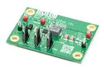
Below is evaluation board with the BD9B300MUV.
Fig 1: BD9B300MUV Evaluation Board
Evaluation Board Schematic
Below is evaluation board schematic for BD9B300MUV.
Fig 2: BD9B300MUV Evaluation Board Schematic
Page 2 of 11
�Application Note
Evaluation Board I/O
Below is reference application circuit that shows the inputs (VIN, Enable, FREQ and MODE) and the output (VOUT).
Fig 3: BD9B300MUV Evaluation Board I/O
Evaluation Board Operation Procedures
Below is the procedure to operate the evaluation board.
1. Connect power supply’s GND terminal to GND test point TP3 on the evaluation board.
2. Connect power supply’s VCC terminal to VIN test point TP2 on the evaluation board. This will provide VIN to the IC U1. Please
note that the VCC should be in range of 2.7V to 5.5V.
3. Set operation mode of IC by set position of shunt jumper of J3 (If Pin2 connect to Pin1, MODE pin of IC U1 will be pulled high
and IC U1 will operate in Fixed frequency PWM mode, else MODE pin of IC U1 will be pulled low and IC U1 will operate in
Automatically switched between the Deep-SLLM control and fixed frequency PWM mode).
4. Set switching frequency of IC by set position of shunt jumper of J2 (If Pin2 connect to Pin1, Frequency pin of IC U1 will be
pulled high and IC U1 will switch frequency of U1 is 1.0MHz, else Frequency pin of IC U1 will be pulled low and IC U1 will
switch frequency of U1 is 2.0MHz).
5. Check if shunt jumper of J1 is at position ON (Pin2 connect to Pin1, EN pin of IC U1 is pulled high).
6. Connect electronic load to TP4 and TP5. Do not turn on load.
7. Turn on power supply. The output voltage VOUT (+3.3V) can be measured at the test point TP4. Now turn on the load. The load
can be increased up to 3A MAX.
Page 3 of 11
�Application Note
Reference Application Data for BD9B300MUV-E2EVK-101
Following graphs show hot plugging test, quiescent current, efficiency, load response, output voltage ripple response of the
BD9B300MUV evaluation board.
Fig 4: Hot Plug-in Test with Zener Diode Fig 5: Circuit Current vs. Power supply
P4SMA6.8A, VIN=5.5V, VOUT=3.3V,
Voltage Characteristics (Temp=25oC,
IOUT=3A, FREQ=L, MODE=L
FREQ=L, MODE=L)
Fig 6: Electric Power Conversion Rate
(VOUT=3.3V, FREQ=L, MODE=L)
Fig 7: Load Response Characteristics
(VIN=5V, VOUT=3.3V, IOUT=0 3A, FREQ=L, MODE=L)
Fig 8: Load Response Characteristics
(VIN=5V, VOUT=3.3V, IOUT=3A 0, FREQ=L, MODE=L)
Fig 9: Output Voltage Ripple Response Characteristics
(VIN=5V, VOUT=3.3V, IOUT=0, FREQ=L, MODE=L)
Fig 10: Output Voltage Ripple Response Characteristics
(VIN=5V, VOUT=3.3V, IOUT=3A, FREQ=L, MODE=L)
Page 4 of 11
�Application Note
Fig 11: Hot Plug-in Test with Zener
Fig 12: Circuit Current vs. Power supply Fig 13: Electric Power Conversion Rate
Diode P4SMA6.8A, VIN=5.5V, VOUT=3.3V, Voltage Characteristics (Temp=25oC,
(VOUT=3.3V, FREQ=L, MODE=H)
IOUT=3A, FREQ=L, MODE=H
FREQ=L, MODE=H)
Fig 14: Load Response Characteristics
(VIN=5V, VOUT=3.3V, IOUT=0 3A, FREQ=L, MODE=H)
Fig 15: Load Response Characteristics
(VIN=5V, VOUT=3.3V, IOUT=3A 0, FREQ=L, MODE=H)
Fig 16: Output Voltage Ripple Response Characteristics
(VIN=5V, VOUT=3.3V, IOUT=0, FREQ=L, MODE=H)
Fig 17: Output Voltage Ripple Response Characteristics
(VIN=5V, VOUT=3.3V, IOUT=3A, FREQ=L, MODE=H)
Page 5 of 11
�Application Note
Fig 19: Circuit Current vs. Power supply Fig 20: Electric Power Conversion Rate
Fig 18: Hot Plug-in Test with Zener
o
Diode P4SMA6.8A, VIN=5.5V, VOUT=3.3V, Voltage Characteristics (Temp=25 C,
(VOUT=3.3V, FREQ=H, MODE=L)
FREQ=H, MODE=L)
IOUT=3A, FREQ=H, MODE=L
Fig 21: Load Response Characteristics
(VIN=5V, VOUT=3.3V, IOUT=0 3A, FREQ=H, MODE=L)
Fig 22: Load Response Characteristics
(VIN=5V, VOUT=3.3V, IOUT=3A 0, FREQ=H, MODE=L)
Fig 23: Output Voltage Ripple Response Characteristics
(VIN=5V, VOUT=3.3V, IOUT=0, FREQ=H, MODE=L)
Fig 24: Output Voltage Ripple Response Characteristics
(VIN=5V, VOUT=3.3V, IOUT=3A, FREQ=H, MODE=L)
Page 6 of 11
�Application Note
Fig 26: Circuit Current vs. Power supply Fig 27: Electric Power Conversion Rate
Fig 25: Hot Plug-in Test with Zener
o
Diode P4SMA6.8A, VIN=5.5V, VOUT=3.3V, Voltage Characteristics (Temp=25 C,
(VOUT=3.3V, FREQ=H, MODE=H)
FREQ=H, MODE=H)
IOUT=3A, FREQ=H, MODE=H
Fig 28: Load Response Characteristics
(VIN=5V, VOUT=3.3V, IOUT=0 3A, FREQ=H, MODE=H)
Fig 29: Load Response Characteristics
(VIN=5V, VOUT=3.3V, IOUT=3A 0, FREQ=H, MODE=H)
Fig 30: Output Voltage Ripple Response Characteristics
(VIN=5V, VOUT=3.3V, IOUT=0, FREQ=H, MODE=H)
Fig 31: Output Voltage Ripple Response Characteristics
(VIN=5V, VOUT=3.3V, IOUT=3A, FREQ=H, MODE=H)
Page 7 of 11
�Application Note
Evaluation Board Layout Guidelines
In the step-down DC/DC converter, a large pulse current flows into two loops. The first loop is the one into which the current
flows when the High-Side FET is turned ON. The flow starts from the input capacitor CIN, runs through the FET, inductor L
and output capacitor COUT and back to GND of CIN via GND of COUT. The second loop is the one into which the current
flows when the Low-Side FET is turned on. The flow starts from the Low-Side FET, runs through the inductor L and output
capacitor COUT and back to GND of the Low-Side FET via GND of COUT. Route these two loops as thick and as short as
possible to allow noise to be reduced for improved efficiency. It is recommended to connect the input and output capacitors
directly to the GND plane. The PCB layout has a great influence on the DC/DC converter in terms of all of the heat
generation, noise and efficiency characteristics.
Fig 32: Current Loop of Buck Converter
Accordingly, design the PCB layout considering the following points.
Connect an input capacitor as close as possible to the IC PVIN terminal on the same plane as the IC.
If there is any unused area on the PCB, provide a copper foil plane for the GND node to assist heat dissipation from the IC
and the surrounding components.
Switching nodes such as SW are susceptible to noise due to AC coupling with other nodes. Route the coil pattern as thick
and as short as possible.
Provide lines connected to FB far from the SW nodes.
Place the output capacitor away from the input capacitor in order to avoid the effect of harmonic noise from the input.
Power Dissipation
When designing the PCB layout and peripheral circuitry, sufficient consideration must be given to ensure that the power
dissipation is within the allowable dissipation curve.
(1) 4-layer board (surface heat dissipation copper foil 5505 mm2)
(Copper foil laminated on each layer)
θJA= 47.0°C/W
(2) 4-layer board (surface heat dissipation copper foil 6.28 mm2)
(Copper foil laminated on each layer)
θJA= 70.62°C/W
(3) 1-layer board (surface heat dissipation copper foil 6.28 mm2)
θJA= 201.6°C/W
(4) IC only
θJA= 462.9°C/W
Fig 33: Thermal Derating Characteristics
Page 8 of 11
�Application Note
Fig 34: BD9B300MUV-E2EVK-101 Board PCB layout
Calculation of Application Circuit Components
Selection of inductor (L)
The inductance significantly depends on output ripple current. As shown by following equation, the ripple current decreases as the
inductor and/or switching frequency increase.
∆𝐈𝐋 =
(𝐕𝐈𝐍 −𝐕𝐎𝐔𝐓 )×𝐕𝐎𝐔𝐓
𝐋×𝐕𝐈𝐍 ×𝐟
f: switching frequency, L: inductance, ΔIL: inductor current ripple
As a minimum requirement, the DC current rating of the inductor should be equal to the maximum load current plus half of the
inductor current ripples as shown by the following equation.
𝐈𝐋𝐏𝐄𝐀𝐊 = 𝐈𝐎𝐔𝐓𝐌𝐀𝐗 +
∆𝐈𝐋
𝟐
Page 9 of 11
�Application Note
Evaluation Board BOM
Below is a table with the build of materials. Part numbers and supplier references are provided.
Item
Qty.
Ref
Description
Manufacturer
Part Number
1
2
3
4
5
6
7
8
9
10
11
12
13
14
15
1
1
3
2
1
1
3
1
1
1
1
1
1
1
3
CR1
C1
C2,C3,C4
C5,C6
C10
D1
J1,J2,J3
L1
Q1
R1
R2
R3
R4
R5
TP1,TP2,TP4
LED 570NM GREEN WTR CLR 0603 SMD
CAP CER 10UF 10V 10% X5R 1206
CAP CER 0.1UF 16V 10% X7R 0603
CAP CER 22UF 6.3V 10% X5R 1210
CAP CER 180PF 50V 5% NP0 0603
DIODE TVS 400W 6.8V UNI 5% SMD
CONN HEADER VERT .100 3POS 15AU
INDUCTOR WW 1.5UH 8A SMD
TRANSISTOR NPN 40V 0.6A SOT-23
RES 140 OHM 1/10W 1% 0603 SMD
RES 100K OHM 1/10W 5% 0603 SMD
RES 1K OHM 1/10W 5% 0603 SMD
RES 160K OHM 1/10W 1% 0603 SMD
RES 51K OHM 1/10W 1% 0603 SMD
TEST POINT PC MULTI PURPOSE RED
SML-310MTT86
GRM319R61A106KE19D
GRM188R71C104KA01D
GRM32DR60J226KA01L
GRM1885C1H181JA01D
P4SMA6.8A
87224-3
74437349015
SST2222AT116
MCR03ERTF1400
MCR03ERTJ104
MCR03ERTJ102
MCR03ERTF1603
MCR03ERTF5102
5010
16
2
TP3,TP5
TEST POINT PC MULTI PURPOSE BLK
Rohm
Murata
Murata
Murata
Murata
Littelfuse Inc
TE Connectivity
Wurth
Rohm
Rohm
Rohm
Rohm
Rohm
Rohm
Keystone
Electronics
Keystone
Electronics
17
18
1
3
U1
TE Connectivity
881545-1
Shunt jumper for header J1, J2, J3 (item
#7), CONN SHUNT 2POS GOLD
W/HANDLE
5011
Page 10 of 11
�Application Note
Notes
No copying or reproduction of this document, in part or in whole, is permitted without the consent of
ROHM Co.,Ltd.
The content specified herein is subject to change for improvement without notice.
The content specified herein is for the purpose of introducing ROHM's products (hereinafter "Products").
If you wish to use any such Product, please be sure to refer to the specifications, which can be obtained
from ROHM upon request.
Examples of application circuits, circuit constants and any other information contained herein illustrate
the standard usage and operations of the Products. The peripheral conditions must be taken into
account when designing circuits for mass production.
Great care was taken in ensuring the accuracy of the information specified in this document. However,
should you incur any damage arising from any inaccuracy or misprint of such information, ROHM shall
bear no responsibility for such damage.
The technical information specified herein is intended only to show the typical functions of and examples
of application circuits for the Products. ROHM does not grant you, explicitly or implicitly, any license to
use or exercise intellectual property or other rights held by ROHM and other parties. ROHM shall bear no
responsibility whatsoever for any dispute arising from the use of such technical information.
The Products specified in this document are intended to be used with general-use electronic equipment
or devices (such as audio visual equipment, office-automation equipment, communication devices,
electronic appliances and amusement devices).
The Products specified in this document are not designed to be radiation tolerant.
While ROHM always makes efforts to enhance the quality and reliability of its Products, a Product may
fail or malfunction for a variety of reasons.
Please be sure to implement in your equipment using the Products safety measures to guard against the
possibility of physical injury, fire or any other damage caused in the event of the failure of any Product,
such as derating, redundancy, fire control and fail-safe designs. ROHM shall bear no responsibility
whatsoever for your use of any Product outside of the prescribed scope or not in accordance with the
instruction manual.
The Products are not designed or manufactured to be used with any equipment, device or system which
requires an extremely high level of reliability the failure or malfunction of which may result in a direct
threat to human life or create a risk of human injury (such as a medical instrument, transportation
equipment, aerospace machinery, nuclear-reactor controller, fuel-controller or other safety device).
ROHM shall bear no responsibility in any way for use of any of the Products for the above special
purposes. If a Product is intended to be used for any such special purpose, please contact a ROHM
sales representative before purchasing.
If you intend to export or ship overseas any Product or technology specified herein that may be
controlled under the Foreign Exchange and the Foreign Trade Law, you will be required to obtain a
license or permit under the Law.
Thank you for your accessing to ROHM product information.
More detail product information and catalogs are available, please contact us.
ROHM Customer Support System
http://www.rohm.com/contact/
Page 11 of 11
�


 工商网监
湘ICP备2023018690号
工商网监
湘ICP备2023018690号
