Datasheet
7.0V〜28V Input, 3A Integrated MOSFET
Single Synchronous Buck DC/DC Converter
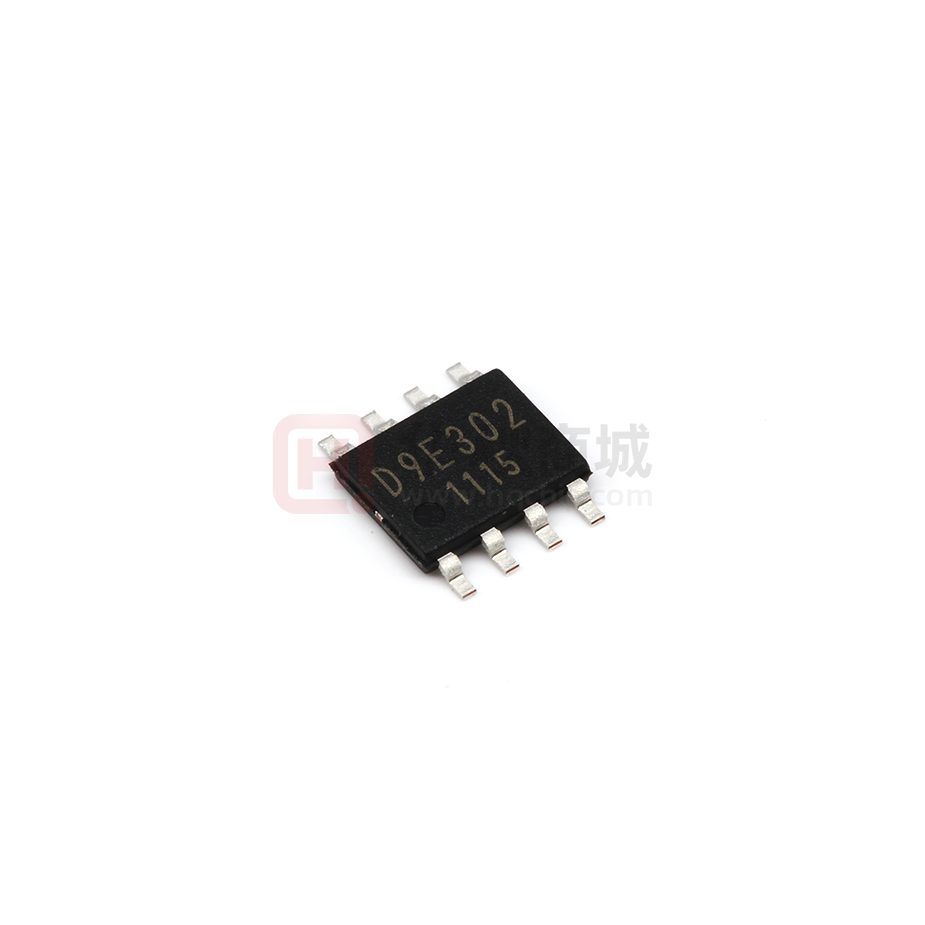
BD9E302EFJ
General Description
BD9E302EFJ is a synchronous buck switching regulator
with built-in power MOSFETs. High efficiency at light load
with a SLLMTM (Simple Light Load Mode). It is most
suitable for use in the equipment to reduce the standby
power is required. It is a current mode control DC/DC
converter and features high-speed transient response.
Phase compensation can also be set easily.
Key Specifications
Features
Synchronous single DC/DC converter
SLLMTM control (Simple Light Load Mode)
Over current protection
Short circuit protection
Thermal shutdown protection
Under voltage lockout protection
Soft start
Reduce external diode
HTSOP-J8 package
Package
Input voltage range:
7.0V to 28V
Output voltage range:
1.0V to VIN x 0.7V
Output current:
3.0 A (Max)
Switching frequency:
550 kHz (Typ)
High-Side MOSFET on-resistance:
90 mΩ (Typ)
Low-Side MOSFET on-resistance:
70 mΩ (Typ)
Shutdown current:
0 μA (Typ)
HTSOP-J8
W (Typ) x D (Typ) x H (Max)
4.90 mm x 6.00 mm x 1.00 mm
Applications
Consumer applications such as home appliance
Secondary power supply and Adapter equipment
Telecommunication devices
HTSOP-J8
Typical Application Circuit
Figure 1. Application circuit
○Product structure:Silicon monolithic integrated circuit.
www.rohm.com
© 2016 ROHM Co., Ltd. All rights reserved.
TSZ22111・14・001
○This product is not designed for protection against radioactive rays.
1/41
TSZ02201-0J3J0AJ00890-1-2
27.Apr.2016 Rev.002
�Datasheet
BD9E302EFJ
Pin Configuration
(TOP VIEW)
BOOT
1
VIN
2
E-Pad
8
SW
7
PGND
EN
3
6
COMP
AGND
4
5
FB
Figure 2. Pin assignment
Pin Descriptions
Pin No.
Pin Name
Description
1
BOOT
2
VIN
Power supply terminal for the switching regulator and control circuit.
Connecting 10 µF+0.1µF ceramic capacitor is recommended.
3
EN
Turning this terminal signal low-level (0.8 V or lower) forces the device to enter the
shutdown mode. Turning this terminal signal high-level (2.5 V or higher) enables the
device. This terminal must be terminated.
4
AGND
5
FB
Connect a bootstrap capacitor of 0.1 µF between this terminal and SW terminal.
The voltage of this capacitor is the gate drive voltage of the high-side MOSFET.
Ground terminal for the control circuit.
Inverting input node for the gm error amplifier.
See page 30 for how to calculate the resistance of the output voltage setting.
6
COMP
Input terminal for the gm error amplifier output and the output switch current comparator.
Connect a frequency phase compensation component to this terminal.
See page 33 for how to calculate the resistance and capacitance for phase
compensation.
7
PGND
Ground terminal for the output stage of the switching regulator.
8
SW
-
E-Pad
Switch node. This terminal is connected to the source of the high-side MOSFET and
drain of the low-side MOSFET. Connect a bootstrap capacitor of 0.1 µF between these
terminals and BOOT terminals. In addition, connect an inductor considering the direct
current superimposition characteristic.
Exposed pad. Connecting this to the internal PCB ground plane using multiple vias
provides excellent heat dissipation characteristics.
www.rohm.com
© 2016 ROHM Co., Ltd. All rights reserved.
TSZ22111•15•001
2/41
TSZ02201-0J3J0AJ00890-1-2
27.Apr.2016 Rev.002
�Datasheet
BD9E302EFJ
Block Diagram
Figure 3. Block diagram
www.rohm.com
© 2016 ROHM Co., Ltd. All rights reserved.
TSZ22111•15•001
3/41
TSZ02201-0J3J0AJ00890-1-2
27.Apr.2016 Rev.002
�Datasheet
BD9E302EFJ
Description of Blocks
VREG3
Block creating internal reference voltage 3V (Typ).
VREG
Block creating internal reference voltage 5V (Typ).
BOOTREG
Block creating gate drive voltage.
TSD
This is thermal shutdown block. Usually IC operating in the allowable power dissipation, but when the IC power dissipation
more than rating value, Tj will increase, when the chip temperature exceeds 175C (Typ), The thermal shutdown circuit is
intended for shutting down internal power devices. Then the Tj will decreased and IC restart. It is not meant to protect or
guarantee the soundness of the application. Do not use the function of this circuit for application protection design.
UVLO
This is under voltage lockout block. Avoid the IC miss operation at low VIN or VIN start up, IC shuts down when VIN under
6.4V (Typ). When UVLO release, the IC restart, Still the threshold voltage has hysteresis of 200mV (Typ).
ERR
The ERR block is an error amplifier and its inputs are the reference voltage 0.8 V (Typ) and the “FB” pin voltage. (Refer to
recommended examples on page 33). The output “COMP” pin controls the switching duty, the output voltage is set by
“FB” pin with external resistors. Moreover, the external resistor and capacitor are required to COMP pin as phase
compensation circuit.
OSC
Block generating oscillation frequency.
SLOPE
Creates delta wave from clock, generated by OSC, and sends voltage composed by current sense signal of high side
MOSFET and delta wave to PWM comparator.
PWM
Settles switching duty by comparing output COMP terminal voltage of error amplifier and signal of SLOPE part.
DRIVER LOGIC
This is DC/DC driver block. Input signal from PWM and drives MOSFET.
SOFT START
By controlling current output voltage starts calmly preventing over shoot of output voltage and inrush current.
OCP
Current flowing in high side MOSFET is controlled one circle each of switching frequency when over current occurs.
SCP
The short circuit protection block compares the FB terminal voltage with the internal standard voltage VREF. When the FB
terminal voltage has fallen below 0.56 V (Typ) and remained there for 0.9 msec (Typ), SCP stops the operation for 14.4
msec (Typ) and subsequently initiates a restart.
OVP
Over voltage protection function (OVP) compares FB terminal voltage with the internal standard voltage VREF. When the
FB terminal voltage exceeds 1.04V (Typ) it turns MOSFET of output part MOSFET OFF. After output voltage drop it
returns with hysteresis.
www.rohm.com
© 2016 ROHM Co., Ltd. All rights reserved.
TSZ22111•15•001
4/41
TSZ02201-0J3J0AJ00890-1-2
27.Apr.2016 Rev.002
�Datasheet
BD9E302EFJ
Absolute Maximum Ratings (Ta = 25C)
Parameter
Symbol
Rating
Unit
Supply Voltage
VIN
-0.3 to +30
V
EN Input Voltage
VEN
-0.3 to VIN
V
Voltage from GND to BOOT
VBOOT
-0.3 to +35
V
Voltage from SW to BOOT
⊿VBOOT
-0.3 to +7
V
VFB
-0.3 to +7
V
VCOMP
-0.3 to +7
V
SW Input Voltage
VSW
-0.5 to VIN +0.3
V
Operating Ambient Temperature Range
Topr
-40 to +85
C
Storage Temperature Range
Tstg
-55 to +150
C
FB Input Voltage
COMP Input Voltage
Caution1: Operating the IC over the absolute maximum ratings may damage the IC. The damage can either be a short circuit between pins or an open circuit
between pins and the internal circuitry. Therefore, it is important to consider circuit protection measures, such as adding a fuse, in case the IC is operated over
the absolute maximum ratings.
Thermal Resistance(Note 1)
Parameter
Symbol
Thermal Resistance (Typ)
1s(Note 3)
2s2p(Note 4)
Unit
HTSOP-J8
Junction to Ambient
θJA
206.4
45.2
°C/W
Junction to Top Characterization Parameter(Note 2)
ΨJT
21
13
°C/W
(Note 1)Based on JESD51-2A(Still-Air)
(Note 2)The thermal characterization parameter to report the difference between junction temperature and the temperature at the top center of the outside
surface of the component package.
(Note 3)Using a PCB board based on JESD51-3.
Layer Number of
Measurement Board
Single
Material
Board Size
FR-4
114.3mm x 76.2mm x 1.57mmt
Top
Copper Pattern
Thickness
Footprints and Traces
70μm
(Note 4)Using a PCB board based on JESD51-5, 7.
Layer Number of
Measurement Board
4 Layers
Thermal Via(NOTE 5)
Material
Board Size
FR-4
114.3mm x 76.2mm x 1.6mmt
Top
2 Internal Layers
Pitch
1.20mm
Diameter
Φ0.30mm
Bottom
Copper Pattern
Thickness
Copper Pattern
Thickness
Copper Pattern
Thickness
Footprints and Traces
70μm
74.2mm x 74.2mm
35μm
74.2mm x 74.2mm
70μm
(Note 5) This thermal via connects with the copper pattern of all layers..
www.rohm.com
© 2016 ROHM Co., Ltd. All rights reserved.
TSZ22111•15•001
5/41
TSZ02201-0J3J0AJ00890-1-2
27.Apr.2016 Rev.002
�Datasheet
BD9E302EFJ
Recommended Operating Ratings
Parameter
Rating
Symbol
Min
Typ
Max
Unit
Supply Voltage
VIN
7.0
-
28
V
Output Current
IOUT
0
-
3.0
A
VRANGE
1.0(Note 1)
-
VIN × 0.7
V
Output Voltage Range
(Note 1) Please use it in I/O voltage setting of which output pulse width does not become 200nsec (Typ) or less.(The output voltage set method,
please refer to Page 30.)
Electrical Characteristics(Ta = 25C, VIN 12 V, VEN = 3 V unless otherwise specified)
Parameter
Symbol
Limits
Min
Typ
Max
Unit
Conditions
Supply Current in Operating
IOPR
-
290
580
µA
VFB = 0.9V
No switching
Supply Current in Standby
ISTBY
-
0
10
µA
VEN = 0V
Reference Voltage
VFB
0.792
0.800
0.808
V
FB Input Current
IFB
-1
0
1
µA
Switching frequency
FOSC
484
550
616
kHz
High-side FET on-resistance
RONH
-
90
-
mΩ
ISW = 100mA
Low-side FET on-resistance
RONL
-
70
-
mΩ
ISW = 100mA
Over Current limit
ILIMIT
-
5.2
-
A
UVLO detection voltage
VUVLO
6.0
6.4
6.7
V
UVLO hysteresis voltage
VUVLOHYS
100
200
300
mV
EN high-level input voltage
VENH
2.5
-
VIN
V
EN low-level input voltage
VENL
0
-
0.8
V
EN Input current
IEN
2
4
8
µA
Soft Start time
TSS
1.2
2.5
5.0
msec
●
VFB = 0.8V
VIN falling
VEN = 3V
VFB : FB Input Voltage. VEN : EN Input Voltage.
www.rohm.com
© 2016 ROHM Co., Ltd. All rights reserved.
TSZ22111•15•001
6/41
TSZ02201-0J3J0AJ00890-1-2
27.Apr.2016 Rev.002
�Datasheet
BD9E302EFJ
650.0
1.0
550.0
0.8
Stand by Current[µA]
Operating Current[µA]
Typical Performance Curves
VIN =28V
450.0
VIN=24V
350.0
250.0
VIN =28V
0.6
VIN =24V
VIN =12V
0.4
VIN =7V
0.2
VIN =12V
VIN =7V
0.0
150.0
-40
-20
0
20
40
60
80
-40
-20
Temperature[°C]
0.816
40
60
80
Figure 5. Stand-by Current - Temperature
1.0
VIN =28V
VIN =12V
VFB =0.8V
0.8
VIN =24V
0.6
VIN =12V
VIN =7V
FB Input Current[µA]
Voltage Reference[V]
20
Temperature[°C]
Figure 4. Operating Current - Temperature
0.808
0
0.800
0.792
0.4
0.2
0.0
-0.2
-0.4
-0.6
-0.8
0.784
-1.0
-40
-20
0
20
40
60
80
-40
Temperature[°C]
0
20
40
60
80
Temperature[°C]
Figure 6. FB Voltage Reference - Temperature
www.rohm.com
© 2016 ROHM Co., Ltd. All rights reserved.
TSZ22111•15•001
-20
Figure 7. FB Input Current - Temperature
7/41
TSZ02201-0J3J0AJ00890-1-2
27.Apr.2016 Rev.002
�Datasheet
BD9E302EFJ
Typical Performance Curves -continued
95.0
682
616
VIN =7V
VIN =12V
VIN =12V
Maximum Duty[%]
Switching Frequency[kHz]
94.5
550
VIN =24V
VIN =7V
VIN =28V
93.5
93.0
VIN =28V
VIN =24V
484
94.0
92.5
92.0
418
-40
-20
0
20
40
60
-40
80
-20
20
40
60
80
Temperature[°C]
Temperature[°C]
Figure 8. Switching Frequency - Temperature
Figure 9. Maximum Duty - Temperature
200
200
VIN =12V
VIN =12V
175
Low Side MOSFET On Resistance[mΩ]
High Side MOSFET On Resistance[mΩ]
0
150
125
100
75
50
25
175
150
125
100
75
50
25
0
0
-40
-20
0
20
40
60
-40
80
0
20
40
60
80
Temperature[°C]
Temperature[°C]
Figure 10. High Side MOSFET On-ResistanceTemperature
www.rohm.com
© 2016 ROHM Co., Ltd. All rights reserved.
TSZ22111•15•001
-20
Figure 11. Low Side MOSFET On-ResistanceTemperature
8/41
TSZ02201-0J3J0AJ00890-1-2
27.Apr.2016 Rev.002
�Datasheet
BD9E302EFJ
Typical Performance Curves -continued
6.9
0.30
6.8
VIN Sweep up
0.25
UVLO Hysteresis[V]
VIN Input Voltage[V]
6.7
6.6
6.5
6.4
6.3
VIN Sweep down
6.2
0.20
0.15
6.1
0.10
6.0
-40
-20
0
20
40
60
-40
80
-20
0
20
40
60
80
Temperature[°C]
Temperature[°C]
Figure 13. UVLO Hysteresis- Temperature
Figure 12. UVLO Threshold - Temperature
8.0
EN=3V
2.3
7.0
6.0
2.0
EN Input Current[µA]
VEN Input Voltage[V]
EN Sweep up
1.7
EN Sweep down
1.4
5.0
4.0
3.0
2.0
1.1
1.0
0.0
0.8
-40
-20
0
20
40
60
-40
80
0
20
40
60
80
Temperature[℃]
Temperature[°C]
Figure 14. EN Threshold - Temperature
www.rohm.com
© 2016 ROHM Co., Ltd. All rights reserved.
TSZ22111•15•001
-20
Figure 15. EN Input Current - Temperature
9/41
TSZ02201-0J3J0AJ00890-1-2
27.Apr.2016 Rev.002
�Datasheet
BD9E302EFJ
Typical Performance Curves -continued
5.0
VIN = 7V
VIN = 12V
Soft Start Time[ms]
4.0
VIN = 24V
VIN = 28V
3.0
2.0
1.0
-40
-20
0
20
40
60
80
Temperature[°C]
Figure 16. Soft Start Time - Temperature
www.rohm.com
© 2016 ROHM Co., Ltd. All rights reserved.
TSZ22111•15•001
10/41
TSZ02201-0J3J0AJ00890-1-2
27.Apr.2016 Rev.002
�Datasheet
BD9E302EFJ
Typical Performance Curves (Application)
VIN=10V/div
VIN=10V/div
EN=10V/div
VOUT=5V/div
EN=10V/div
Time=2ms/div
Time=2ms/div
SW=10V/div
VOUT=5V/div
SW=10V/div
Figure 17. Power Up (VIN = EN)
Figure 18. Power Down (VIN = EN)
VIN=10V/div
VIN=10V/div
EN=5V/div
EN=5V/div
VOUT=5V/div
VOUT=5V/div
Time=1ms/div
Time=200us/div
SW=10V/div
SW=10V/div
Figure 19. Power Up (EN = 0V→5V,Io=3A)
www.rohm.com
© 2016 ROHM Co., Ltd. All rights reserved.
TSZ22111•15•001
Figure 20. Power Down (EN = 5V→0V,Io=3A)
11/41
TSZ02201-0J3J0AJ00890-1-2
27.Apr.2016 Rev.002
�Datasheet
BD9E302EFJ
Typical Performance Curves (Application)-continue
VOUT=50mV/div
SW=5V/div
VOUT=20mV/div
Time=40ms/div
SW=5V/div
Figure 22. VOUT Ripple
(VIN = 12V, VOUT = 5V, IOUT = 3A)
Figure 21. VOUT Ripple
(VIN = 12V, VOUT = 5V, IOUT = 0A)
VIN=100mV/div
VIN=50mV/div
SW=5V/div
Time=40ms/div
SW=5V/div
Time=2µs/div
Figure 24. VIN Ripple
(VIN = 12V, VOUT = 5V, IOUT = 3A)
Figure 23. VIN Ripple
(VIN = 12V, VOUT = 5V, IOUT = 0A)
www.rohm.com
© 2016 ROHM Co., Ltd. All rights reserved.
TSZ22111•15•001
Time=1µs/div
12/41
TSZ02201-0J3J0AJ00890-1-2
27.Apr.2016 Rev.002
�Datasheet
BD9E302EFJ
Typical Performance Curves (Application)-continue
IL=1A/div
SW=5V/div
IL=1A/div
Time=1µs/div
SW=10V/div
Figure 25. Switching Waveform
(VIN = 12V, VOUT = 5V, IOUT = 3A)
Time=1µs/div
Figure 26. Switching Waveform
(VIN = 24V, VOUT = 5V, IOUT = 3A)
IL=1A/div
Time=4µs/div
SW=5V/div
SLLMTM control
Figure 27. Switching Waveform
(VIN = 12V, VOUT = 5V, IOUT = 50mA)
www.rohm.com
© 2016 ROHM Co., Ltd. All rights reserved.
TSZ22111•15•001
13/41
TSZ02201-0J3J0AJ00890-1-2
27.Apr.2016 Rev.002
�Datasheet
BD9E302EFJ
2.0
2.0
1.5
1.5
1.0
1.0
Output Voltage Change[%]
Output Voltage Change[%]
Typical Performance Curves (Application)-continue
0.5
0.0
-0.5
-1.0
VOUT = 3.3V
Io=3A
-1.5
0.5
0.0
-0.5
-1.0
VOUT = 5V
Io=3A
-1.5
-2.0
-2.0
6
8
10 12 14 16 18 20 22 24 26 28
6
8
10 12 14 16 18 20 22 24 26 28
VIN Input Voltage[V]
VIN Input Voltage[V]
Figure 29. VOUT Line Regulation
(VOUT = 5V)
2.0
2.0
1.5
1.5
1.0
1.0
Output Voltage Change[%]
Output Voltage Change[%]
Figure 28. VOUT Line Regulation
(VOUT = 3.3V)
0.5
0.0
-0.5
-1.0
VIN = 24V
VOUT = 3.3V
-1.5
0.5
0.0
-0.5
-1.0
VIN = 24V
VOUT = 5.0V
-1.5
-2.0
-2.0
0.0
0.5
1.0
1.5
2.0
2.5
3.0
Output Current[A]
0.5
1.0
1.5
2.0
2.5
3.0
Output Current[A]
Figure 31. VOUT Load Regulation
(VOUT = 5V)
Figure 30. VOUT Load Regulation
(VOUT = 3.3V)
www.rohm.com
© 2016 ROHM Co., Ltd. All rights reserved.
TSZ22111•15•001
0.0
14/41
TSZ02201-0J3J0AJ00890-1-2
27.Apr.2016 Rev.002
�Datasheet
BD9E302EFJ
Function Description
1) DC/DC converter operation
BD9E302EFJ is a synchronous rectifying step-down switching regulator that achieves faster transient response by
employing current mode PWM control system. It utilizes switching operation in PWM (Pulse Width Modulation) mode
for heavier load, while it utilizes SLLM (Simple Light Load Mode) control for lighter load to improve efficiency.
Efficiency η[%]
① SLLMTM control
② PWM control
Output current IOUT[A]
Figure 32. Efficiency (SLLMTM control and PWM control)
②PWM control
①SLLMTM control
VOUT =100mV/div
SW=5V/div
VOUT =50mV/div
Time=4µs/div
SW=5V/div
Figure 33. SW Waveform (①SLLMTM control)
(VIN = 12V, VOUT = 5.0V, IOUT = 50mA)
www.rohm.com
© 2016 ROHM Co., Ltd. All rights reserved.
TSZ22111•15•001
Time=4µs/div
Figure 34. SW Waveform (②PWM control)
(VIN = 12V, VOUT = 5.0V, IOUT = 3A)
15/41
TSZ02201-0J3J0AJ00890-1-2
27.Apr.2016 Rev.002
�Datasheet
BD9E302EFJ
2) Enable Control
The IC shutdown can be controlled by the voltage applied to the EN terminal. When EN voltage reaches 2.5 V, the
internal circuit is activated and the IC starts up. To enable shutdown control with the EN terminal, set the shutdown
interval (Low level interval of EN) must be set to 100 µs or longer.
EN terminal
Output setting voltage
Figure 35. Timing Chart with Enable Control
3) Protective Functions
The protective circuits are intended for prevention of damage caused by unexpected accidents. Do not use them
for continuous protective operation.
3-1) Short Circuit Protection (SCP)
The short circuit protection block compares the FB terminal voltage with the internal reference voltage VREF. When
the FB terminal voltage has fallen below 0.56 V (Typ) and remained there for 0.9 msec (Typ), SCP stops the operation
for 14.4 msec (Typ) and subsequently initiates a restart.
Table 1. Short Circuit Protection Function
EN pin
FB pin
Short Circuit Protection
Switching Frequency
0.30V (Typ)≥FB
2.5 V or higher
137.5kHz (Typ)
0.30V (Typ)< FB≤0.56V (Typ)
Enabled
275kHz (Typ)
FB>0.56V (Typ)
0.8 V or lower
550kHz (Typ)
-
Disabled
OFF
Figure 36. Short circuit protection function (SCP) timing chart
www.rohm.com
© 2016 ROHM Co., Ltd. All rights reserved.
TSZ22111•15•001
16/41
TSZ02201-0J3J0AJ00890-1-2
27.Apr.2016 Rev.002
�Datasheet
BD9E302EFJ
3-2) Under Voltage Lockout Protection (UVLO)
The under voltage lockout protection circuit monitors the VIN terminal voltage.
The operation enters standby when the VIN terminal voltage is 6.4 V (Typ) or lower.
The operation starts when the VIN terminal voltage is 6.6 V (Typ) or higher.
VIN
UVLO
ON
UVLO
OFF
hys
0V
VOUT
VOUT×0.85
Soft start
FB
High-side
MOSFET gate
Low-side
MOSFET gate
Normal operation
UVLO
Normal operation
Figure 37. UVLO Timing Chart
3-3) Thermal Shutdown Function (TSD)
This is thermal shutdown block. Usually IC operating in the allowable power dissipation, but when the IC power
dissipation more than rating value, Tj will increase, when the chip temperature exceeds 175C(Typ), The thermal
shutdown circuit is intended to shut down internal power devices. Then the Tj will decreased and IC restart. It is not
meant to protect or guarantee the soundness of the application. Do not use the function of this circuit for application
protection design.
3-4) Over Current Protection Function (OCP)
The overcurrent protection function is realized by using the current mode control to limit the current that flows through
the high-side MOSFET at each cycle of the switching frequency.
3-5) Over Voltage Protection Function (OVP)
Over voltage protection function (OVP) compares FB terminal voltage with internal standard voltage VREF and when FB
terminal voltage exceeds1.04V (Typ) it turns MOSFET of output part MOSFET OFF. After output voltage drop it returns
with hysteresis.
www.rohm.com
© 2016 ROHM Co., Ltd. All rights reserved.
TSZ22111•15•001
17/41
TSZ02201-0J3J0AJ00890-1-2
27.Apr.2016 Rev.002
�Datasheet
BD9E302EFJ
Application Example 1
Parameter
Input Voltage
Output Voltage
Switching Frequency
Maximum Output Current
Operating Ambient Temperature Range
Symbol
VIN
VOUT
FOSC
IOMAX
Topr
Value Example
12/24 V
5V
550kHz(Typ)
3A
-40 °C ~ +85°C
CBOOT
L
1
BOOT
2
VIN
3
EN
SW
8
PGND
7
COMP
6
FB
5
COUT
VOUT
VIN
CIN
BD9E302EFJ
C2
R3
R1
CIN1
4
AGND
R2
Figure 38. Application Circuit 1
Table 2. Recommendation Circuit constants
Reference
Designator
R1
Configuration
(mm)
1005
Specification
Part Number
Type
Manufacturer
430 kΩ, 1 %, 1 / 16 W
MCR01MZPF4303
Chip resistor
ROHM
R2
1005
82 kΩ, 1 %, 1 / 16 W
MCR01MZPF8202
Chip resistor
ROHM
R3
1005
10 kΩ, 5 %, 1 / 16 W
MCR01MZPJ103
Chip resistor
ROHM
C2
1005
6800 pF R, 50 V
GRM series
Ceramic capacitor
MURATA
CBOOT
1608
0.1 μF, B, 50 V
GRM series
Ceramic capacitor
MURATA
CIN1(Note 1)
1608
0.1 μF, B, 50 V
GRM series
Ceramic capacitor
MURATA
CIN(Note 2)
3225
10 μF, B, 50 V
GRM series
Ceramic capacitor
MURATA
COUT(Note 3)
3225
22 μF B, 25 V × 2
GRM series
Ceramic capacitor
MURATA
L
7269
4.7μH
CLF7045NIT-4R7N
Inductor
TDK
(Note 1) In order to reduce the influence of high frequency noise, arrange the 0.1μF ceramic capacitor as close as possible to the VIN pin.
(Note 2) For capacitance of input capacitor, take temperature characteristics, DC bias characteristics, etc. into consideration to set minimum value to no less
than 4.7μF.
(Note 3) In case capacitance value fluctuates due to temperature characteristics, DC bias characteristics, etc. of output capacitor, crossover frequency may
fluctuate. When selecting a capacitor, confirm the characteristics of the capacitor in its datasheet.Also, Please use capacitors such as ceramic type
are recommended for output capacitor.
www.rohm.com
© 2016 ROHM Co., Ltd. All rights reserved.
TSZ22111•15•001
18/41
TSZ02201-0J3J0AJ00890-1-2
27.Apr.2016 Rev.002
�Datasheet
100
100
90
90
80
80
70
70
Efficiency[%]
Efficiency[%]
BD9E302EFJ
60
50
40
60
50
40
30
30
20
20
10
10
0
0
1
10
100
1000
10000
1
10
1000
10000
Output Current[mA]
Output Current[mA]
Figure 40. Efficiency - Output Current
(VIN=24V, VOUT = 5.0V, R3=10kΩ)
Figure 39. Efficiency - Output Current
(VIN=12V, VOUT = 5.0V, R3=10kΩ)
VOUT =50mV/div@AC
VOUT =50mV/div@AC
Time =2μs/div
Time =2μs/div
SW =5V/div
SW =10V/div
Figure 42. VOUT Ripple
(VIN = 24V, VOUT = 5V, R3=10kΩ)
Figure 41. VOUT Ripple
(VIN = 12V, VOUT = 5V, R3=10kΩ)
www.rohm.com
© 2016 ROHM Co., Ltd. All rights reserved.
TSZ22111•15•001
100
19/41
TSZ02201-0J3J0AJ00890-1-2
27.Apr.2016 Rev.002
�Datasheet
BD9E302EFJ
VOUT=300mV/div
VOUT=300mV/div
Slew Rate : 0.01A/μs
IOUT=1A/div
Slew Rate : 0.01A/μs
IOUT=1A/div
Time=5ms/div
Figure 43. Load Transient Response IOUT=1.5A - 3A
(VIN=12V, VOUT=5V, R3=10kΩ)
Figure 44. Load Transient Response IOUT=1.5A - 3A
(VIN=24V, VOUT=5V, R3=10kΩ)
Figure 46. Loop Response IOUT=3A
(VIN=24V, VOUT=5V, R3=10kΩ)
Figure 45. Loop Response IOUT=3A
(VIN=12V, VOUT=5V, R3=10kΩ)
www.rohm.com
© 2016 ROHM Co., Ltd. All rights reserved.
TSZ22111•15•001
Time=5ms/div
20/41
TSZ02201-0J3J0AJ00890-1-2
27.Apr.2016 Rev.002
�Datasheet
BD9E302EFJ
Application Example 2 (Fast load response)
Parameter
Input Voltage
Output Voltage
Switching Frequency
Maximum Output Current
Operating Ambient Temperature Range
Symbol
VIN
VOUT
FOSC
IOMAX
Topr
Value Example
12/24 V
5V
550kHz(Typ)
3A
-40 °C ~ +85°C
BD9E302EFJ
Figure 47. Application Circuit 2
Table 3. Recommendation Circuit constants
Reference
Designator
R1
Configuration
(mm)
1005
Specification
Part Number
Type
Manufacturer
430 kΩ, 1 %, 1 / 16 W
MCR01MZPF4303
Chip resistor
ROHM
R2
1005
82 kΩ, 1 %, 1 / 16 W
MCR01MZPF8202
Chip resistor
ROHM
R3
1005
15 kΩ, 5 %, 1 / 16 W
MCR01MZPJ153
Chip resistor
ROHM
C1
1005
18 pF CH, 50 V
GRM series
Ceramic capacitor
MURATA
C2
1005
6800 pF R, 50 V
GRM series
Ceramic capacitor
MURATA
CBOOT
1608
0.1 μF, B, 50 V
GRM series
Ceramic capacitor
MURATA
(Note 1)
1608
0.1 μF, B, 50 V
GRM series
Ceramic capacitor
MURATA
CIN(Note 2)
3225
10 μF, B, 50 V
GRM series
Ceramic capacitor
MURATA
(Note 3)
3225
22 μF B, 25 V × 2
GRM series
Ceramic capacitor
MURATA
L
7269
4.7μH
CLF7045NIT-4R7N
Inductor
TDK
CIN1
COUT
(Note 1) In order to reduce the influence of high frequency noise, arrange the 0.1μF ceramic capacitor as close as possible to the VIN pin.
(Note 2) For capacitance of input capacitor, take temperature characteristics, DC bias characteristics, etc. into consideration to set minimum value to no less
than 4.7μF.
(Note 3) In case capacitance value fluctuates due to temperature characteristics, DC bias characteristics, etc. of output capacitor, crossover frequency may
fluctuate. When selecting a capacitor, confirm the characteristics of the capacitor in its datasheet.Also, Please use capacitors such as ceramic type
are recommended for output capacitor.
www.rohm.com
© 2016 ROHM Co., Ltd. All rights reserved.
TSZ22111•15•001
21/41
TSZ02201-0J3J0AJ00890-1-2
27.Apr.2016 Rev.002
�Datasheet
100
100
90
90
80
80
70
70
Efficiency[%]
Efficiency[%]
BD9E302EFJ
60
50
40
60
50
40
30
30
20
20
10
10
0
0
1
10
100
1000
10000
1
10
1000
10000
Output Current[mA]
Output Current[mA]
Figure 48. Efficiency - Output Current
(VIN=12V, VOUT = 5.0V, R3=15kΩ, C1=18pF)
Figure 49. Efficiency - Output Current
(VIN=24V, VOUT = 5.0V, R3=15kΩ, C1=18pF
VOUT =50mV/div@AC
VOUT =50mV/div@AC
Time =2μs/div
Time =2μs/div
SW =5V/div
SW =10V/div
Figure 51. VOUT Ripple
(VIN = 24V, VOUT = 5V, R3=15kΩ, C1=18pF)
Figure 50. VOUT Ripple
(VIN = 12V, VOUT = 5V, R3=15kΩ, C1=18pF)
www.rohm.com
© 2016 ROHM Co., Ltd. All rights reserved.
TSZ22111•15•001
100
22/41
TSZ02201-0J3J0AJ00890-1-2
27.Apr.2016 Rev.002
�Datasheet
BD9E302EFJ
VOUT=200mV/div
VOUT=200mV/div
Slew Rate: 0.5A/us
IOUT=1A/div
Slew Rate: 0.5A/us
IOUT=1A/div
Time=200us/div
Figure 53. Load Transient Response IOUT=1.5A - 3A
(VIN=24V, VOUT=5V, R3=15kΩ, C1=18pF)
Figure 52. Load Transient Response IOUT=1.5A - 3A
(VIN=12V, VOUT=5V, R3=15kΩ, C1=18pF)
Figure 54. Loop Response IOUT=3A
(VIN=12V, VOUT=5V, R3=15kΩ, C1=18pF)
www.rohm.com
© 2016 ROHM Co., Ltd. All rights reserved.
TSZ22111•15•001
Time=200us/div
Figure 55. Loop Response IOUT=3A
(VIN=24V, VOUT=5V, R3=15kΩ, C1=18pF)
23/41
TSZ02201-0J3J0AJ00890-1-2
27.Apr.2016 Rev.002
�Datasheet
BD9E302EFJ
Application Example 3
Parameter
Input Voltage
Output Voltage
Switching Frequency
Maximum Output Current
Operating Ambient Temperature Range
Symbol
VIN
VOUT
FOSC
IOMAX
Topr
Value Example
12/24 V
3.3 V
550kHz(Typ)
3A
-40 °C ~ +85°C
CBOOT
L
1
BOOT
2
VIN
3
EN
SW
8
PGND
7
COMP
6
FB
5
COUT
VOUT
VIN
CIN
BD9E302EFJ
C2
CIN1
4
AGND
R3
R1
R2
Figure 56. Application Circuit 3
Table 4. Recommendation Circuit constants
Reference
Designator
R1
Configuration
(mm)
1005
Specification
Part Number
Type
Manufacturer
75 kΩ, 1 %, 1 / 16 W
MCR01MZPF7502
Chip resistor
ROHM
R2
1005
24 kΩ, 1 %, 1 / 16 W
MCR01MZPF2402
Chip resistor
ROHM
R3
1005
6.8 kΩ, 5 %, 1 / 16 W
MCR01MZPJ682
Chip resistor
ROHM
C2
1005
6800 pF R, 50 V
GRM series
Ceramic capacitor
MURATA
CBOOT
1608
0.1 μF, B, 50 V
GRM series
Ceramic capacitor
MURATA
CIN1(Note 1)
1608
0.1 μF, B, 50 V
GRM series
Ceramic capacitor
MURATA
CIN(Note 2)
3225
10 μF, B, 50 V
GRM series
Ceramic capacitor
MURATA
COUT(Note 3)
3225
22 μF B, 25 V × 2
GRM series
Ceramic capacitor
MURATA
L
7269
3.3μH
CLF7045NIT-3R3N
Inductor
TDK
(Note 1) In order to reduce the influence of high frequency noise, arrange the 0.1μF ceramic capacitor as close as possible to the VIN pin.
(Note 2) For capacitance of input capacitor, take temperature characteristics, DC bias characteristics, etc. into consideration to set minimum value to no less
than 4.7μF.
(Note 3) In case capacitance value fluctuates due to temperature characteristics, DC bias characteristics, etc. of output capacitor, crossover frequency may
fluctuate. When selecting a capacitor, confirm the characteristics of the capacitor in its datasheet.Also, Please use capacitors such as ceramic type
are recommended for output capacitor.
www.rohm.com
© 2016 ROHM Co., Ltd. All rights reserved.
TSZ22111•15•001
24/41
TSZ02201-0J3J0AJ00890-1-2
27.Apr.2016 Rev.002
�Datasheet
100
100
90
90
80
80
70
70
Efficiency[%]
Efficiency[%]
BD9E302EFJ
60
50
40
60
50
40
30
30
20
20
10
10
0
0
1
10
100
1000
10000
1
10
Output Current[mA]
1000
10000
Output Current[mA]
Figure 58. Efficiency - Output Current
(VIN=24V, VOUT = 3.3V, R3=6.8kΩ)
Figure 57. Efficiency - Output Current
(VIN=12V, VOUT = 3.3V, R3=6.8kΩ)
VOUT =50mV/div@AC
VOUT =50mV/div@AC
Time =2us/div
Time =2us/div
SW =5V/div
SW =10V/div
Figure 60. VOUT Ripple
(VIN = 24V, VOUT = 3.3V, R3=6.8kΩ)
Figure 59. VOUT Ripple
(VIN = 12V, VOUT = 3.3V, R3=6.8kΩ)
www.rohm.com
© 2016 ROHM Co., Ltd. All rights reserved.
TSZ22111•15•001
100
25/41
TSZ02201-0J3J0AJ00890-1-2
27.Apr.2016 Rev.002
�Datasheet
BD9E302EFJ
VOUT=300mV/div
VOUT=300mV/div
Slew Rate : 0.01A/μs
Slew Rate : 0.01A/μs
IOUT=1A/div
IOUT=1A/div
Time=5ms/div
Figure 61. Load Transient Response IOUT=1.5A - 3A
(VIN=12V, VOUT=3.3V, R3=6.8kΩ)
Figure 62. Load Transient Response IOUT=1.5A - 3A
(VIN=24V, VOUT=3.3V, R3=6.8kΩ)
Figure 64. Loop Response IOUT=3A
(VIN=24V, VOUT=3.3V, R3=6.8kΩ)
Figure 63. Loop Response IOUT=3A
(VIN=12V, VOUT=3.3V, R3=6.8kΩ)
www.rohm.com
© 2016 ROHM Co., Ltd. All rights reserved.
TSZ22111•15•001
Time=5ms/div
26/41
TSZ02201-0J3J0AJ00890-1-2
27.Apr.2016 Rev.002
�Datasheet
BD9E302EFJ
Application Example 4 (Fast load response)
Parameter
Input Voltage
Output Voltage
Switching Frequency
Maximum Output Current
Operating Ambient Temperature Range
Symbol
VIN
VOUT
FOSC
IOMAX
Topr
Value Example
12/24 V
3.3 V
550kHz(Typ)
3A
-40 °C ~ +85°C
BD9E302EFJ
Figure 65. Application Circuit 4
Table 5. Recommendation Circuit constants
Reference
Designator
R1
Configuration
(mm)
1005
Specification
Part Number
Type
Manufacturer
75 kΩ, 1 %, 1 / 16 W
MCR01MZPF7502
Chip resistor
ROHM
R2
1005
24 kΩ, 1 %, 1 / 16 W
MCR01MZPF2402
Chip resistor
ROHM
R3
1005
10 kΩ, 5 %, 1 / 16 W
MCR01MZPJ103
Chip resistor
ROHM
C1
1005
100 pF CH, 50 V
GRM series
Ceramic capacitor
MURATA
C2
1005
6800 pF R, 50 V
GRM series
Ceramic capacitor
MURATA
CBOOT
1608
0.1 μF, B, 50 V
GRM series
Ceramic capacitor
MURATA
(Note 1)
1608
0.1 μF, B, 50 V
GRM series
Ceramic capacitor
MURATA
CIN(Note 2)
3225
10 μF, B, 50 V
GRM series
Ceramic capacitor
MURATA
(Note 3)
3225
22 μF B, 25 V × 2
GRM series
Ceramic capacitor
MURATA
L
7269
3.3μH
CLF7045NIT-3R3N
Inductor
TDK
CIN1
COUT
(Note 1) In order to reduce the influence of high frequency noise, arrange the 0.1μF ceramic capacitor as close as possible to the VIN pin.
(Note 2) For capacitance of input capacitor, take temperature characteristics, DC bias characteristics, etc. into consideration to set minimum value to no less
than 4.7μF.
(Note 3) In case capacitance value fluctuates due to temperature characteristics, DC bias characteristics, etc. of output capacitor, crossover frequency may
fluctuate. When selecting a capacitor, confirm the characteristics of the capacitor in its datasheet.Also, Please use capacitors such as ceramic type
are recommended for output capacitor.
www.rohm.com
© 2016 ROHM Co., Ltd. All rights reserved.
TSZ22111•15•001
27/41
TSZ02201-0J3J0AJ00890-1-2
27.Apr.2016 Rev.002
�Datasheet
100
100
90
90
80
80
70
70
Efficiency[%]
Efficiency[%]
BD9E302EFJ
60
50
40
60
50
40
30
30
20
20
10
10
0
0
1
10
100
1000
10000
1
Output Current[mA]
100
1000
10000
Output Current[mA]
Figure 67. Efficiency - Output Current
(VIN=24V, VOUT = 3.3V, R3=10kΩ, C1=100pF)
Figure 66. Efficiency - Output Current
(VIN=12V, VOUT = 3.3V, R3=10kΩ, C1=100pF)
VOUT =50mV/div@AC
VOUT =50mV/div@AC
Time =2μs/div
Time =2μs/div
SW =5V/div
SW =10V/div
Figure 68. VOUT Ripple
(VIN = 12V, VOUT = 3.3V, R3=6.8kΩ, C1=100pF)
www.rohm.com
© 2016 ROHM Co., Ltd. All rights reserved.
TSZ22111•15•001
10
Figure 69. VOUT Ripple
(VIN = 24V, VOUT = 3.3V, R3=6.8kΩ,C1=100pF)
28/41
TSZ02201-0J3J0AJ00890-1-2
27.Apr.2016 Rev.002
�Datasheet
BD9E302EFJ
VOUT=200mV/div
VOUT=200mV/div
Slew Rate: 0.5A/μs
IOUT=1A/div
Slew Rate: 0.5A/μs
IOUT=1A/div
Time=200μs/div
Figure 70. Load Transient Response IOUT=1.5A - 3A
(VIN=12V, VOUT=3.3V, R3=10kΩ, C1=100pF)
Figure 71. Load Transient Response IOUT=1.5A - 3A
(VIN=24V, VOUT=3.3V, R3=10kΩ, C1=100pF)
Figure 73. Loop Response IOUT=3A
(VIN=24V, VOUT=3.3V, R3=10kΩ, C1=100pF)
Figure 72. Loop Response IOUT=3A
(VIN=12V, VOUT=3.3V, R3=10kΩ, C1=100pF)
www.rohm.com
© 2016 ROHM Co., Ltd. All rights reserved.
TSZ22111•15•001
Time=200μs/div
29/41
TSZ02201-0J3J0AJ00890-1-2
27.Apr.2016 Rev.002
�Datasheet
BD9E302EFJ
Selection of Components Externally Connected
About the application except the recommendation, please contact us.
Parameters required to design a power supply are as follows.
Parameter
Input Voltage
Output Voltage
Switching Frequency
Inductor ripple current
ESR of the output capacitor
Output capacitor
Soft-start time
Max output current
Symbol
VIN
VOUT
FOSC
∆IL
RESR
COUT
TSS
IOMAX
Value Example
24 V
5V
550kHz(Typ)
1.13A
10mΩ
44μF(22μF×2)
2.5ms(Typ)
3A
1. Switching Frequency
Switching frequency is fixed to FOSC = 550kHz (Typ).
2. Output Voltage Set Point
The output voltage value can be set by the feedback resistance ratio.
V OUT
※
R1
R2
R2
0.8 [V]
Minimum pulse range that can be produced at the output
stably through all the load area is 200nsec for
BD9E302EFJ.
Use input/output condition which satisfies the following
method.
V OUT
200 nsec ≤
V IN FOSC
Figure 74. Feedback Resistor Circuit
Please set feedback resistor R1 + R2 below 700 kΩ . In addition, since power efficiency is reduced with a small R1 + R2,
please set the current flowing through the feedback resistor to be small as possible than the output current IO.
3. Input capacitor configuration
For input capacitor, use a ceramic capacitor. It will more effective as close as possible to the VIN pin. The rating voltage of
input capacitor should be 2 times of VIN supply and 1.2 times of maximum VIN supply is commanded. For normal setting,
10μF is recommended, but with larger value, input ripple voltage can be further reduced. Also, for capacitance of input
capacitor, take temperature characteristics, DC bias characteristics, etc. into consideration, minimum value no less than
4.7μF. In order to reduce the influence of high frequency noise, 0.1μF ceramic capacitor placed as close as possible to the
VIN pin is commanded.
www.rohm.com
© 2016 ROHM Co., Ltd. All rights reserved.
TSZ22111•15•001
30/41
TSZ02201-0J3J0AJ00890-1-2
27.Apr.2016 Rev.002
�Datasheet
BD9E302EFJ
4. Output LC Filter
The DC/DC converter requires an LC filter for smoothing the output voltage in order to supply a continuous current to the
load. Selecting an inductor with large inductance causes the ripple current ∆IL that flows into the inductor to be small,
decreasing the ripple voltage generated in the output voltage, it is a trade-off of size and cost of the inductor. In BD9E302EFJ,
the ripple current feedback to IC, and internal SLLMTM(Simple Light Load Mode)control it, Since the optimal operation
feedback ripple current designed based on the recommended inductance, please use recommended inductor values.
.
VIN
IL
Inductor saturation current > IOUTMAX +∆IL /2
∆IL
IOUTMAX
L
Driver
Average inductor current
VOUT
COUT
t
Figure 75. Waveform of current through inductor
Figure 76. Output LC filter circuit
Here, select an inductance so that the size of the ripple current component of the inductor will be 20% to 50% of the Max
output current (3A).
Now calculating with VIN = 12V, VOUT = 5V, switching frequency FOSC = 550kHz, ∆IL is1.0A, inductance value
That can be used is calculated as follows:
L
V OUT
1
V IN ‐ V OUT
V IN
FOSC
ΔI L
5.3 ≒ 4.7 μH
* If the output voltage setting is larger than half of VIN please calculated as follows:
L
4
V IN
FOSC
ΔI L
Also for saturation current of inductor, select the one with larger current than maximum output current added by 1/2 of
inductor ripple current ∆IL.
Output capacitor COUT affects output ripple voltage characteristics. Select output capacitor COUT so that necessary ripple
voltage characteristics are satisfied.
Output ripple voltage can be expressed in the following method.
ΔV RPL
ΔI L
R ESR
1
8 C OUT FOSC
RESR is the equivalent series resistance of the output capacitor
With COUT = 44µF, RESR = 10mΩ the output ripple voltage is calculated as
ΔV RPL
1.0
10m
8
1
44μ
550k
15.17 [mV]
End the calculation.
www.rohm.com
© 2016 ROHM Co., Ltd. All rights reserved.
TSZ22111•15•001
31/41
TSZ02201-0J3J0AJ00890-1-2
27.Apr.2016 Rev.002
�Datasheet
BD9E302EFJ
* When selecting the value of the output capacitor COUT, please use ceramic capacitor and please note that the value
of capacitor CLOAD connected to VOUT will be added up to the value of COUT. Charging current to flow through the
CLOAD, COUT when the IC startup, must be completed this charge within the soft-start time. Over-current protection
circuit operates when charging is continued beyond the soft-start time, the IC may not start. The maximum CLOAD that
can be connected to VOUT is calculated by the equation below.
Inductor ripple current maximum value of start-up (ILSTART)
<
Over Current Protection Threshold 4.16 [A](Min)
Inductor ripple current maximum value of start-up (ILSTART) can be expressed in the following method.
ILSTART = Output maximum load current(IOMAX) + Charging current to the output capacitor (ICAP) +
∆IL
2
Charging current to the output capacitor (ICAP) can be expressed in the following method.
I CAP
C OUT
C LOAD
TSS
V OUT
From the above equation, VIN = 12V, VOUT = 5V, L = 4.7μH, IOMAX = 3.0A (Max), switching frequency FOSC = 484kHz (Min),
∆IL=1.282A (Max), the output capacitor COUT = 44μF, TSS = 1.2ms soft-start time (Min), it becomes the following equation
when calculating the maximum output load capacitance CLOAD (Max) that can be connected to VOUT.
C LOAD Max
4.16 ‐ I OMAX ‐ ΔI L /2
V OUT
TSS
‐ C OUT
80.56
[ μF]
5. Input voltage start-up
Figure 77. Input Voltage Start-up Time
Soft-start function is designed for the IC so that the output voltage will start according to the time that was decided
internally. After UVLO release, the output voltage range will be less than 70% of the input voltage at soft-start operation.
Please be sure that the input voltage of the soft-start after startup is as follows.
V
V IN ≥ OUT
0.85
[V]
0.7
www.rohm.com
© 2016 ROHM Co., Ltd. All rights reserved.
TSZ22111•15•001
32/41
TSZ02201-0J3J0AJ00890-1-2
27.Apr.2016 Rev.002
�Datasheet
BD9E302EFJ
6. Phase Compensation
A current mode control buck DC/DC converter is a one-pole, one-zero system. The poles are formed by an error amplifier
and the one load and the one zero point is added by the phase compensation. The phase compensation resistor R3
determines the crossover frequency FCRS(20kHz (Typ)) where the total loop gain of the DC/DC converter is 0 dB. The high
value of this crossover frequency FCRS provides a good load transient response characteristic but inferior stability.
Conversely, specifying a low value for the crossover frequency FCRS greatly stabilizes the characteristics but the load
transient response characteristic is impaired.
(1) Selection of Phase Compensation Resistor R3
The phase compensation resistance R3 can be determined by using the following equation.
2π
R3
V OUT
V FB
FCRS
G MP
C OUT
G MA
[Ω]
where :
VOUT is the output voltage
FCRS is the crossover frequency
C OUT is the output capacitanc e
VFB is the feedback reference voltage (0.8 V (Typ))
G MP is the current sense gain (20A/V (Typ))
G MA is the error amplifier transcondu ctance (140 μA/V (Typ))
*The actual FCRS may different from the value in equation due to DC bias characteristics of COUT .
Please set R3 base on the actual evaluation.
(2) Selection of phase compensation capacitance C2
For stable operation of the DC/DC converter, inserting a zero point under 1/6 of the zero crossover frequency cancels
the phase delay due to the pole formed by the load often, thus, providing favorable characteristics.
Please use capacitors for C2 such as ceramic type.
The phase compensation capacitance C2 can be determined by using the following equation.
C2
2π
1
R3
FZ
[F]
where
FZ is the
Zero point inserted
* In case C2 calculated result exceeds 0.015μF, set the value of compensation capacitance C2 0.015μF. Setting too
large C2 value maybe cause startup failure etc.
(3) Selection of Phase Compensation Capacitance C1
Adding zero point at 20 kHz is recommended to get a better transient load response characteristic for DC/DC
converter. Please use capacitors for C1 such as ceramic type, and set value below 1000pF.
C1 can be determined by the following equation.
C1
1
2π
R1
20kHz
F
(4) Loop stability
In order to ensure stability of DC/DC converter, confirm there is enough phase margin on actual equipment.
Under the worst condition, it is recommended to ensure phase margin is 45° or more. In fact, the characteristics may
variable due to PCB layout, routing of wiring, types of used components and operating environments (temperature
etc.). Use gain-phase analyzer or FRA to confirm frequency characteristics on actual equipment. Contact the
manufacturer of each measuring equipment to check its measuring method, etc.
7. Bootstrap capacitor
Bootstrap capacitor CBOOT shall be 0.1μF. Connect a bootstrap capacitor between SW pin and BOOT pin.
For capacitance of Bootstrap capacitor, take temperature characteristics, DC bias characteristics, etc. into consideration.
www.rohm.com
© 2016 ROHM Co., Ltd. All rights reserved.
TSZ22111•15•001
33/41
TSZ02201-0J3J0AJ00890-1-2
27.Apr.2016 Rev.002
�Datasheet
BD9E302EFJ
PCB Layout Design
In the buck DC/DC converter, a large pulsed current flows in two loops. The first loop is the one into which the current flows
when the High Side FET is turned on. The flow starts from the input capacitor CIN, runs through the FET, inductor L and
output capacitor COUT and back to ground of CIN via ground of COUT. The second loop is the one into which the current flows
when the Low Side FET is turned on. The flow starts from the Low Side FET, runs through the inductor L and output
capacitor COUT and back to ground of the Low Side FET via ground of COUT. Tracing these two loops as thick and short as
possible allows noise to be reduced for improved efficiency. It is recommended to connect the input and output capacitors,
in particular, to the ground plane. The PCB layout has a great influence on the DC/DC converter in terms of all of the heat
generation, noise and efficiency characteristics.
Figure 78. Current loop of buck converter
Accordingly, design the PCB layout with particular attention paid to the following points.
Provide the input capacitor close to the IC VIN terminal as possible on the same plane as the IC.
If there is any unused area on the PCB, provide a copper foil plane for the ground node to assist heat dissipation from
the IC and the surrounding components.
Switching nodes such as SW are susceptible to noise due to AC coupling with other nodes. Trace to the coil as thick
and as short as possible.
Provide lines connected to FB and COMP as far from the SW node.
COMP terminal is sensitive to high frequency harmonic noise, it is recommended that the external components of this
terminal placed close to the pin.
Provide the output capacitor away from the input capacitor in order to avoid the effect of harmonic noise from the
input.
SW1
OFF EN ON
-
+
OFF EN ON
J2
GND
VOUT
C5
TP4
TP3
TP4
TP3
C4
TP2
GND
-
GND
TP2
TP5
PGND
EN
COMP
AGND
FB
C6
TP5
VIN
SW
VIN
R3
TP1
R1
R2
+
VIN
BOOT
TP1
C7
R4
C2
C3
J1
L1
C1
TP6
C8
TP6
ROHM
SEMICONDUCTOR
EVK026
Top Layer
Bottom Layer
Figure 79. Example of sample board layout pattern
www.rohm.com
© 2016 ROHM Co., Ltd. All rights reserved.
TSZ22111•15•001
34/41
TSZ02201-0J3J0AJ00890-1-2
27.Apr.2016 Rev.002
�Datasheet
BD9E302EFJ
I/O Equivalence Circuit
1. BOOT
8. SW
3. EN
BOOTREG
BOOT
VIN
SW
REG
PGND
5. FB
6. COMP
FB
AGND
Figure 80. I/O equivalence circuit
www.rohm.com
© 2016 ROHM Co., Ltd. All rights reserved.
TSZ22111•15•001
35/41
TSZ02201-0J3J0AJ00890-1-2
27.Apr.2016 Rev.002
�Datasheet
BD9E302EFJ
Operational Notes
1.
Reverse Connection of Power Supply
Connecting the power supply in reverse polarity can damage the IC. Take precautions against reverse polarity when
connecting the power supply, such as mounting an external diode between the power supply and the IC’s power
supply pins.
2.
Power Supply Lines
Design the PCB layout pattern to provide low impedance supply lines. Separate the ground and supply lines of the
digital and analog blocks to prevent noise in the ground and supply lines of the digital block from affecting the analog
block. Furthermore, connect a capacitor to ground at all power supply pins. Consider the effect of temperature and
aging on the capacitance value when using electrolytic capacitors.
3.
Ground Voltage
Ensure that no pins are at a voltage below that of the ground pin at any time, even during transient condition. However,
pins that drive inductive loads (e.g. motor driver outputs, DC-DC converter outputs) may inevitably go below ground
due to back EMF or electromotive force. In such cases, the user should make sure that such voltages going below
ground will not cause the IC and the system to malfunction by examining carefully all relevant factors and conditions
such as motor characteristics, supply voltage, operating frequency and PCB wiring to name a few.
4.
Ground Wiring Pattern
When using both small-signal and large-current ground traces, the two ground traces should be routed separately but
connected to a single ground at the reference point of the application board to avoid fluctuations in the small-signal
ground caused by large currents. Also ensure that the ground traces of external components do not cause variations
on the ground voltage. The ground lines must be as short and thick as possible to reduce line impedance.
5.
Thermal Consideration
Should by any chance the maximum junction temperature rating be exceeded the rise in temperature of the chip may
result in deterioration of the properties of the chip. In case of exceeding this absolute maximum rating, increase the
board size and copper area to prevent exceeding the maximum junction temperature rating.
6.
Recommended Operating Conditions
These conditions represent a range within which the expected characteristics of the IC can be approximately obtained.
The electrical characteristics are guaranteed under the conditions of each parameter.
7.
Inrush Current
When power is first supplied to the IC, it is possible that the internal logic may be unstable and inrush current may flow
instantaneously due to the internal powering sequence and delays, especially if the IC has more than one power
supply. Therefore, give special consideration to power coupling capacitance, power wiring, width of ground wiring, and
routing of connections.
8.
Operation Under Strong Electromagnetic Field
Operating the IC in the presence of a strong electromagnetic field may cause the IC to malfunction.
www.rohm.com
© 2016 ROHM Co., Ltd. All rights reserved.
TSZ22111•15•001
36/41
TSZ02201-0J3J0AJ00890-1-2
27.Apr.2016 Rev.002
�Datasheet
BD9E302EFJ
Operational Notes – continued
9.
Testing on Application Boards
When testing the IC on an application board, connecting a capacitor directly to a low-impedance output pin may
subject the IC to stress. Always discharge capacitors completely after each process or step. The IC’s power supply
should always be turned off completely before connecting or removing it from the test setup during the inspection
process. To prevent damage from static discharge, ground the IC during assembly and use similar precautions during
transport and storage.
10. Inter-pin Short and Mounting Errors
Ensure that the direction and position are correct when mounting the IC on the PCB. Incorrect mounting may result in
damaging the IC. Avoid nearby pins being shorted to each other especially to ground, power supply and output pin.
Inter-pin shorts could be due to many reasons such as metal particles, water droplets (in very humid environment) and
unintentional solder bridge deposited in between pins during assembly to name a few.
11. Unused Input Pins
Input pins of an IC are often connected to the gate of a MOS transistor. The gate has extremely high impedance and
extremely low capacitance. If left unconnected, the electric field from the outside can easily charge it. The small charge
acquired in this way is enough to produce a significant effect on the conduction through the transistor and cause
unexpected operation of the IC. So unless otherwise specified, unused input pins should be connected to the power
supply or ground line.
12. Regarding the Input Pin of the IC
This monolithic IC contains P+ isolation and P substrate layers between adjacent elements in order to keep them
isolated. P-N junctions are formed at the intersection of the P layers with the N layers of other elements, creating a
parasitic diode or transistor. For example (refer to figure below):
When GND > Pin A and GND > Pin B, the P-N junction operates as a parasitic diode.
When GND > Pin B, the P-N junction operates as a parasitic transistor.
Parasitic diodes inevitably occur in the structure of the IC. The operation of parasitic diodes can result in mutual
interference among circuits, operational faults, or physical damage. Therefore, conditions that cause these diodes to
operate, such as applying a voltage lower than the GND voltage to an input pin (and thus to the P substrate) should be
avoided.
Figure 81. Example of monolithic IC structure
13. Ceramic Capacitor
When using a ceramic capacitor, determine the dielectric constant considering the change of capacitance with
temperature and the decrease in nominal capacitance due to DC bias and others.
14. Area of Safe Operation (ASO)
Operate the IC such that the output voltage, output current, and the maximum junction temperature rating are all within
the Area of Safe Operation (ASO).
www.rohm.com
© 2016 ROHM Co., Ltd. All rights reserved.
TSZ22111•15•001
37/41
TSZ02201-0J3J0AJ00890-1-2
27.Apr.2016 Rev.002
�Datasheet
BD9E302EFJ
Operational Notes – continued
15. Thermal Shutdown Circuit(TSD)
This IC has a built-in thermal shutdown circuit that prevents heat damage to the IC. Normal operation should always
be within the IC’s maximum junction temperature rating. If however the rating is exceeded for a continued period, the
junction temperature (Tj) will rise which will activate the TSD circuit that will turn OFF all output pins. When the Tj falls
below the TSD threshold, the circuits are automatically restored to normal operation.
Note that the TSD circuit operates in a situation that exceeds the absolute maximum ratings and therefore, under no
circumstances, should the TSD circuit be used in a set design or for any purpose other than protecting the IC from
heat damage.
16. Over Current Protection Circuit (OCP)
This IC incorporates an integrated overcurrent protection circuit that is activated when the load is shorted. This
protection circuit is effective in preventing damage due to sudden and unexpected incidents. However, the IC should
not be used in applications characterized by continuous operation or transitioning of the protection circuit.
www.rohm.com
© 2016 ROHM Co., Ltd. All rights reserved.
TSZ22111•15•001
38/41
TSZ02201-0J3J0AJ00890-1-2
27.Apr.2016 Rev.002
�Datasheet
BD9E302EFJ
Ordering Information
B
D
9
E
3
Part Number
0
2
E
F
J
Package
EFJ: HTSOP-J8
-
E2
Packaging and forming
specification
E2: Embossed tape and reel
Marking Diagram
HTSOP-J8(TOP VIEW)
Part Number Marking
D 9 E 3 0 2
LOT Number
1PIN MARK
www.rohm.com
© 2016 ROHM Co., Ltd. All rights reserved.
TSZ22111•15•001
39/41
TSZ02201-0J3J0AJ00890-1-2
27.Apr.2016 Rev.002
�Datasheet
BD9E302EFJ
●Physical Dimension, Tape and Reel Information – continued
Package Name
HTSOP-J8
Tape
Embossed carrier tape
Quantity
2500pcs
Direction
of feed
E2
The direction is the 1pin of product is at the upper left when you hold
( reel on the left hand and you pull out the tape on the right hand
Direction of feed
1pin
Reel
www.rohm.com
© 2016 ROHM Co., Ltd. All rights reserved.
TSZ22111•15•001
)
∗ Order quantity needs to be multiple of the minimum quantity.
40/41
TSZ02201-0J3J0AJ00890-1-2
27.Apr.2016 Rev.002
�Datasheet
BD9E302EFJ
●Revision History
Date
Revision
22. Jan. ’16
001
27.Apr.2016
002
Description
New
Page.5 Thermal Resistance - Footprints and Traces
74.2mm2 (Square)
⇒
74.2mm x 74.2mm
www.rohm.com
© 2016 ROHM Co., Ltd. All rights reserved.
TSZ22111•15•001
41/41
TSZ02201-0J3J0AJ00890-1-2
27.Apr.2016 Rev.002
�Notice
Precaution on using ROHM Products
1.
Our Products are designed and manufactured for application in ordinary electronic equipments (such as AV equipment,
OA equipment, telecommunication equipment, home electronic appliances, amusement equipment, etc.). If you
(Note 1)
intend to use our Products in devices requiring extremely high reliability (such as medical equipment
, transport
equipment, traffic equipment, aircraft/spacecraft, nuclear power controllers, fuel controllers, car equipment including car
accessories, safety devices, etc.) and whose malfunction or failure may cause loss of human life, bodily injury or
serious damage to property (“Specific Applications”), please consult with the ROHM sales representative in advance.
Unless otherwise agreed in writing by ROHM in advance, ROHM shall not be in any way responsible or liable for any
damages, expenses or losses incurred by you or third parties arising from the use of any ROHM’s Products for Specific
Applications.
(Note1) Medical Equipment Classification of the Specific Applications
JAPAN
USA
EU
CHINA
CLASSⅢ
CLASSⅡb
CLASSⅢ
CLASSⅢ
CLASSⅣ
CLASSⅢ
2.
ROHM designs and manufactures its Products subject to strict quality control system. However, semiconductor
products can fail or malfunction at a certain rate. Please be sure to implement, at your own responsibilities, adequate
safety measures including but not limited to fail-safe design against the physical injury, damage to any property, which
a failure or malfunction of our Products may cause. The following are examples of safety measures:
[a] Installation of protection circuits or other protective devices to improve system safety
[b] Installation of redundant circuits to reduce the impact of single or multiple circuit failure
3.
Our Products are designed and manufactured for use under standard conditions and not under any special or
extraordinary environments or conditions, as exemplified below. Accordingly, ROHM shall not be in any way
responsible or liable for any damages, expenses or losses arising from the use of any ROHM’s Products under any
special or extraordinary environments or conditions. If you intend to use our Products under any special or
extraordinary environments or conditions (as exemplified below), your independent verification and confirmation of
product performance, reliability, etc, prior to use, must be necessary:
[a] Use of our Products in any types of liquid, including water, oils, chemicals, and organic solvents
[b] Use of our Products outdoors or in places where the Products are exposed to direct sunlight or dust
[c] Use of our Products in places where the Products are exposed to sea wind or corrosive gases, including Cl2,
H2S, NH3, SO2, and NO2
[d] Use of our Products in places where the Products are exposed to static electricity or electromagnetic waves
[e] Use of our Products in proximity to heat-producing components, plastic cords, or other flammable items
[f] Sealing or coating our Products with resin or other coating materials
[g] Use of our Products without cleaning residue of flux (even if you use no-clean type fluxes, cleaning residue of
flux is recommended); or Washing our Products by using water or water-soluble cleaning agents for cleaning
residue after soldering
[h] Use of the Products in places subject to dew condensation
4.
The Products are not subject to radiation-proof design.
5.
Please verify and confirm characteristics of the final or mounted products in using the Products.
6.
In particular, if a transient load (a large amount of load applied in a short period of time, such as pulse. is applied,
confirmation of performance characteristics after on-board mounting is strongly recommended. Avoid applying power
exceeding normal rated power; exceeding the power rating under steady-state loading condition may negatively affect
product performance and reliability.
7.
De-rate Power Dissipation depending on ambient temperature. When used in sealed area, confirm that it is the use in
the range that does not exceed the maximum junction temperature.
8.
Confirm that operation temperature is within the specified range described in the product specification.
9.
ROHM shall not be in any way responsible or liable for failure induced under deviant condition from what is defined in
this document.
Precaution for Mounting / Circuit board design
1.
When a highly active halogenous (chlorine, bromine, etc.) flux is used, the residue of flux may negatively affect product
performance and reliability.
2.
In principle, the reflow soldering method must be used on a surface-mount products, the flow soldering method must
be used on a through hole mount products. If the flow soldering method is preferred on a surface-mount products,
please consult with the ROHM representative in advance.
For details, please refer to ROHM Mounting specification
Notice-PGA-E
© 2015 ROHM Co., Ltd. All rights reserved.
Rev.003
�Precautions Regarding Application Examples and External Circuits
1.
If change is made to the constant of an external circuit, please allow a sufficient margin considering variations of the
characteristics of the Products and external components, including transient characteristics, as well as static
characteristics.
2.
You agree that application notes, reference designs, and associated data and information contained in this document
are presented only as guidance for Products use. Therefore, in case you use such information, you are solely
responsible for it and you must exercise your own independent verification and judgment in the use of such information
contained in this document. ROHM shall not be in any way responsible or liable for any damages, expenses or losses
incurred by you or third parties arising from the use of such information.
Precaution for Electrostatic
This Product is electrostatic sensitive product, which may be damaged due to electrostatic discharge. Please take proper
caution in your manufacturing process and storage so that voltage exceeding the Products maximum rating will not be
applied to Products. Please take special care under dry condition (e.g. Grounding of human body / equipment / solder iron,
isolation from charged objects, setting of Ionizer, friction prevention and temperature / humidity control).
Precaution for Storage / Transportation
1.
Product performance and soldered connections may deteriorate if the Products are stored in the places where:
[a] the Products are exposed to sea winds or corrosive gases, including Cl2, H2S, NH3, SO2, and NO2
[b] the temperature or humidity exceeds those recommended by ROHM
[c] the Products are exposed to direct sunshine or condensation
[d] the Products are exposed to high Electrostatic
2.
Even under ROHM recommended storage condition, solderability of products out of recommended storage time period
may be degraded. It is strongly recommended to confirm solderability before using Products of which storage time is
exceeding the recommended storage time period.
3.
Store / transport cartons in the correct direction, which is indicated on a carton with a symbol. Otherwise bent leads
may occur due to excessive stress applied when dropping of a carton.
4.
Use Products within the specified time after opening a humidity barrier bag. Baking is required before using Products of
which storage time is exceeding the recommended storage time period.
Precaution for Product Label
A two-dimensional barcode printed on ROHM Products label is for ROHM’s internal use only.
Precaution for Disposition
When disposing Products please dispose them properly using an authorized industry waste company.
Precaution for Foreign Exchange and Foreign Trade act
Since concerned goods might be fallen under listed items of export control prescribed by Foreign exchange and Foreign
trade act, please consult with ROHM in case of export.
Precaution Regarding Intellectual Property Rights
1.
All information and data including but not limited to application example contained in this document is for reference
only. ROHM does not warrant that foregoing information or data will not infringe any intellectual property rights or any
other rights of any third party regarding such information or data.
2.
ROHM shall not have any obligations where the claims, actions or demands arising from the combination of the
Products with other articles such as components, circuits, systems or external equipment (including software).
3.
No license, expressly or implied, is granted hereby under any intellectual property rights or other rights of ROHM or any
third parties with respect to the Products or the information contained in this document. Provided, however, that ROHM
will not assert its intellectual property rights or other rights against you or your customers to the extent necessary to
manufacture or sell products containing the Products, subject to the terms and conditions herein.
Other Precaution
1.
This document may not be reprinted or reproduced, in whole or in part, without prior written consent of ROHM.
2.
The Products may not be disassembled, converted, modified, reproduced or otherwise changed without prior written
consent of ROHM.
3.
In no event shall you use in any way whatsoever the Products and the related technical information contained in the
Products or this document for any military purposes, including but not limited to, the development of mass-destruction
weapons.
4.
The proper names of companies or products described in this document are trademarks or registered trademarks of
ROHM, its affiliated companies or third parties.
Notice-PGA-E
© 2015 ROHM Co., Ltd. All rights reserved.
Rev.003
�