Datasheet
4.5V to 28V Input, 8.0A Integrated MOSFET
Single Synchronous Buck DC/DC Converter
BD9F800MUX-Z
Key Specifications
General Description
BD9F800MUX-Z is a synchronous buck DC/DC converter
with built-in low on-resistance power MOSFETs. It is
capable of providing current of up to 8 A. External phase
compensation circuit is not necessary for it is a constant
on-time control DC/DC converter with high speed
response.
Input Voltage Range:
4.5V to 28 V
Output Voltage Setting Range:
0.765V to 13.5V
Output Current:
8 A (Max)
Switching Frequency:
300kHz or 600kHz (Typ)
High Side MOSFET On-Resistance: 23 m Ω (Typ)
Low Side MOSFET On-Resistance: 11 m Ω (Typ)
Shutdown Current:
2 μA (Typ)
Features
Package
Synchronous Single DC/DC Converter
Constant On-time Control
Over Current Protection
Short Circuit Protection
Thermal Shutdown Protection
Under Voltage Lockout Protection
Power Good Output
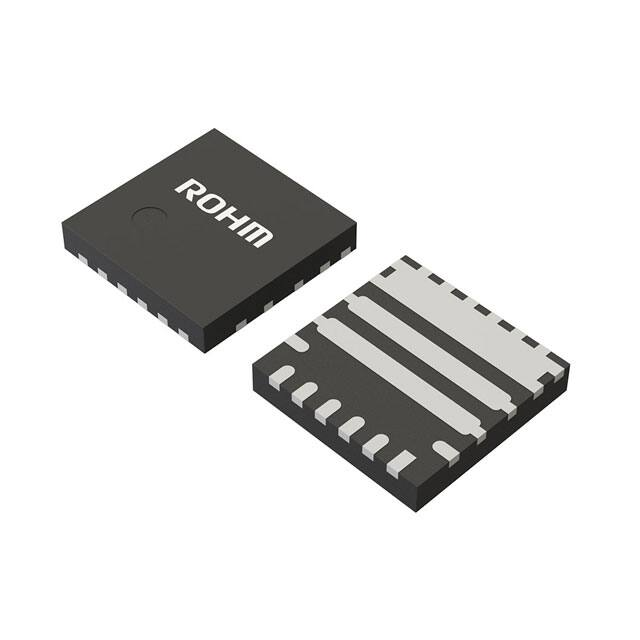
VQFN11X3535A Package
VQFN11X3535A
W (Typ) × D (Typ) × H (Max)
3.50mm × 3.50mm × 0.60mm
Applications
Step-down Power Supply for DSPs,
Microprocessors, etc.
Set-top Box
LCD TVs
DVD / Blu-ray Player / Recorder
Entertainment Devices
VQFN11X3535A
Typical Application Circuit
BD9F800MUX-Z
VIN
VIN
CIN
Enable
EN
BOOT
CBOOT
PGND
VOUT
SW
FREQ
VOUT
RFREQ
VREG
CVREG
PGD
L
R1
FB
GND
COUT
R2
Figure 1. Typical Application Circuit
○Product structure: Silicon monolithic integrated circuit ○This product has no designed protection against radioactive rays.
www.rohm.com
TSZ02201-0F3F0AC00090-1-2
© 2017 ROHM Co., Ltd. All rights reserved.
1/47
27.Dec.2018 Rev.003
TSZ22111 • 14 • 001
�BD9F800MUX-Z
Pin Configuration
1. BOOT
2. PGD
3. VOUT
4. FREQ
5. FB
6. VREG
(TOP VIEW)
7. GND
11. EN
8. VIN
9. SW
10. PGND
Figure 2. Pin Configuration
Pin Descriptions
Terminal
No.
Symbol
1
BOOT
2
PGD
Power Good terminal. It is necessary to connect a pull-up resistor due to an open drain
output. See page 19 for how to specify the resistance. When the FB terminal voltage is within
±7% of 0.765V (Typ), the internal Nch MOSFET turns off and the output turns High.
3
VOUT
Output voltage sense terminal.
Connect a 10Ω resistor in series when output voltage setting is more than 3.3V.
4
FREQ
Switching frequency setting terminal.
Switching frequency is set to 300kHz when this terminal is set to Low (0.8V or lower). Setting
this terminal to High (2.2V or higher) will make switching frequency set to 600kHz. This
terminal needs to be pulled down to ground or pulled up to VREG by 10kΩ.
5
FB
6
VREG
7
GND
Ground terminal for the control circuit.
8
VIN
Power supply terminal for the switching regulator.
Connecting 20µF(10µF×2) and 0.1µF ceramic capacitor to ground is recommended.
9
SW
Switch terminal. The SW terminal is connected to the source of the High-Side MOSFET and
drain of the Low-Side MOSFET. Connect a bootstrap capacitor of 0.1µF between BOOT and
SW terminal. Also, connect an inductor considering the direct current superimposition
characteristic.
10
PGND
11
EN
Function
Bootstrap terminal.
Connect a ceramic capacitor of 0.1µF between BOOT and SW terminal.
The voltage of this capacitor is the gate drive voltage of the High-Side MOSFET.
An inverting input node for the error amplifier and main comparator.
To calculate for the resistance value of the output voltage setting, refer to page 39.
Internal power supply voltage terminal.
A voltage of 5.25V (Typ) is outputted if there is more than 2.3V for EN terminal.
Connect a ceramic capacitor of 2.2µF to ground.
Ground terminal for the output stage of the switching regulator.
Enable terminal.
Turning this terminal signal Low (0.7V or lower) forces the device to enter in shutdown mode.
Turning this terminal signal High (2.3V or higher) enables the device. This terminal must be
properly terminated.
www.rohm.com
© 2017 ROHM Co., Ltd. All rights reserved.
TSZ22111 • 15 • 001
2/47
TSZ02201-0F3F0AC00090-1-2
27.Dec.2018 Rev.003
�BD9F800MUX-Z
Block Diagram
EN
11
VREG
63
8 VIN
VIN
EN
EN
VREG
VREG
VREG
REF
VREF
VREF
1 BOOT
SW
On Time
Controller
Block
FREQ 4
VOUT 3
Error
Amplifier
R
Q
EN
S
SW
Main
Comparator
REF
SS
OCPH
Driver
Circuit
9
SW
VREG
OCPL
FB 5
10 PGND
UVLO
UVLO
TSD
UVLO
2 PGD
SCP
EN
UVLO
TSD
SCP
SCP
Thermal
Protection
Soft
Start
TSD
FB
VREF
PGOOD
SS
7
GND
Figure 3. Block Diagram
www.rohm.com
© 2017 ROHM Co., Ltd. All rights reserved.
TSZ22111 • 15 • 001
3/47
TSZ02201-0F3F0AC00090-1-2
27.Dec.2018 Rev.003
�BD9F800MUX-Z
Description of Blocks
●
EN
The device will shut down when EN falls to 0.7V (Max) or lower. When EN reaches 2.3V (Min), the internal circuit is
activated and the device starts up.
●
VREG
The VREG block generates the internal power supply.
●
VREF
The VREF block generates the internal reference voltage.
●
Error Amplifier
Error Amplifier adjusts Main Comparator input to make internal reference voltage equal to FB terminal voltage.
●
Main Comparator
Main comparator compares Error Amplifier output and FB terminal voltage. When FB terminal voltage becomes low, it
outputs High and reports to the On Time block that the output voltage has dropped below control voltage.
●
ON Time Controller Block
This block generates ON Time. The desired ON Time is generated when Main Comparator output becomes High. ON
Time is adjusted to restrict frequency change even with Input / Output voltage change.
●
Soft Start
The Soft Start circuit slows down the rise of output voltage during start-up and controls the current, which allows the
prevention of output voltage overshoot and inrush current. The internal soft start time is set to 1ms typically.
●
PGOOD
When the FB terminal voltage reaches within ±7% of 0.765V(Typ), the built-in open drain output Nch MOSFET turns
off and the output goes high.
●
Driver Circuit
This block is a DC/DC driver. A signal from ON Time Controller Block is applied to drive the MOSFETs.
●
UVLO
UVLO is a protection circuit that prevents low voltage malfunction. It prevents malfunction of the internal circuit from
sudden rise and fall of power supply voltage. When VIN voltage is higher than 4.2V (Typ), UVLO is released and the
soft-start circuit will be started. This threshold voltage has a hysteresis of 400mV (Typ). When VIN voltage is less than
3.8V (Typ), the device will shut down.
●
TSD
The TSD block is for thermal protection. The thermal protection circuit shuts down the device when the internal
temperature of device rises to 175°C (Typ) or higher. Thermal protection circuit resets when the temperature falls. The
circuit has a hysteresis of 25°C (Typ).
●
SCP
After the soft start is completed and when the FB terminal voltage has fallen below 0.38V (Typ) for 250μs (Typ), the
SCP stops the operation for 8ms (Typ) and subsequently initiates restart.
●
OCPH
When inductor current exceeds the current limit threshold value while High-Side MOSFET is ON, the High-Side
MOSFET will turn OFF.
●
OCPL
The OCP function limits the current flowing through the Low-Side MOSFET for every switching period. If the inductor
current exceeds the source current limit threshold value IOCP while Low-Side MOSFET is ON, the Low-Side MOSFET
remains ON even with FB voltage is lower than the REF voltage. The Low-Side MOSFET keeps ON until inductor
current becomes lower than IOCP and High-Side MOSFET will turn ON. The Low-Side MOSFET will turn OFF when
inductor current exceeds the sink current limit threshold value while Low-Side MOSFET is ON.
www.rohm.com
© 2017 ROHM Co., Ltd. All rights reserved.
TSZ22111 • 15 • 001
4/47
TSZ02201-0F3F0AC00090-1-2
27.Dec.2018 Rev.003
�BD9F800MUX-Z
Absolute Maximum Ratings (Ta = 25C)
Parameter
Symbol
Rating
Unit
VIN
-0.3 to +30
V
VBOOT
-0.3 to +35
V
VBOOT - VSW
-0.3 to +7
V
SW Terminal Voltage
VSW
-0.3 to VIN + 0.3
V
FB Terminal Voltage
VFB
-0.3 to VVREG
V
VREG Terminal Voltage
VVREG
-0.3 to +6
V
FREQ Terminal Voltage
VFREQ
-0.3 to +7
V
VOUT Terminal Voltage
VVOUT
-0.3 to +20
V
PGD Terminal Voltage
VPGD
-0.3 to +35
V
Input Voltage
Voltage from GND to BOOT
Voltage from SW to BOOT
EN Terminal Voltage
Maximum Junction Temperature
VEN
-0.3 to +30
V
Tjmax
150
°C
Tstg
-55 to +150
°C
Storage Temperature Range
Caution 1: Operating the IC over the absolute maximum ratings may damage the IC. The damage can either be a short circuit between pins or an open circuit
between pins and the internal circuitry. Therefore, it is important to consider circuit protection measures, such as adding a fuse, in case the IC is operated over
the absolute maximum ratings.
Caution 2: Should by any chance the maximum junction temperature rating be exceeded the rise in temperature of the chip may result in deterioration of the
properties of the chip. In case of exceeding this absolute maximum rating, increase the board size and copper area to prevent exceeding the maximum junction
temperature rating.
Thermal Resistance(Note 1)
Parameter
Symbol
Thermal Resistance (Typ)
1s(Note 3)
2s2p(Note 4)
Unit
VQFN11X3535A
Junction to Ambient
θJA
232.1
48.0
°C/W
Junction to Top Characterization Parameter(Note 2)
ΨJT
44.2
8.2
°C/W
(Note 1) Based on JESD51-2A(Still-Air).
(Note 2) The thermal characterization parameter to report the difference between junction temperature and the temperature at the top center of the outside
surface of the component package.
(Note 3) Using a PCB board based on JESD51-3.
Layer Number of
Measurement Board
Single
Material
Board Size
FR-4
114.3mm x 76.2mm x 1.57mmt
Top
Copper Pattern
Thickness
Footprints and Traces
70μm
(Note 4) Using a PCB board based on JESD51-7.
Layer Number of
Measurement Board
4 Layers
Material
Board Size
FR-4
114.3mm x 76.2mm x 1.6mmt
Top
2 Internal Layers
Thermal Via(Note 5)
Pitch
Diameter
1.20mm
Φ0.30mm
Bottom
Copper Pattern
Thickness
Copper Pattern
Thickness
Copper Pattern
Thickness
Footprints and Traces
70μm
74.2mm x 74.2mm
35μm
74.2mm x 74.2mm
70μm
(Note 5) This thermal via connects with the copper pattern of all layers.
www.rohm.com
© 2017 ROHM Co., Ltd. All rights reserved.
TSZ22111 • 15 • 001
5/47
TSZ02201-0F3F0AC00090-1-2
27.Dec.2018 Rev.003
�BD9F800MUX-Z
Recommended Operating Conditions
Parameter
Input Voltage
Operating Temperature Range
Output Current
Output Voltage Range
Symbol
Min
Typ
Max
Unit
VIN
4.5
12
28
V
Topr
+85
(Note 1)
-40
-
°C
IOUT
0
-
8
A
VRANGE
0.765 (Note 2)
-
13.5 (Note 3)
V
(Note 1) Tj must be lower than 150°C under actual operating environment. Life time is derated at junction temperature greater than125°C.
(Note 2) Please use under the condition of VOUT≥VIN×0.033 [V] (300kHz), VOUT ≥VIN×0.067 [V] (600kHz).
(Note 3) Please use under the condition of VOUT≤VIN×0.87-0.12×IOUT [V](300kHz), VOUT ≤VIN×0.77-0.13×IOUT [V](600kHz).
(Refer to the page 39 for how to calculate the output voltage setting.)
Electrical Characteristics (Ta = 25°C, VIN = 12V, VEN = 3V, FREQ=L unless otherwise specified)
Parameter
Symbol
Min
Typ
Max
Unit
Shutdown Current
ISD
-
2
15
µA
Operating Circuit Current
IVIN
-
0.85
1.6
mA
Conditions
VEN=GND
IOUT=0mA
when no switching
EN Low Voltage
VENL
-
-
0.7
V
EN High Voltage
VENH
2.3
-
VIN
V
EN Input Current
IEN
-
2.5
10
µA
FREQ Low Voltage
VFREQL
-
-
0.8
V
FREQ High Voltage
VFREQH
2.2
-
VVREG
V
FREQ Input Current
IFREQ
-
1.5
5
µA
VFREQ=3V
VVREG_SD
-
-
0.1
V
VEN=GND
VREG Output Voltage
VVREG
5
5.25
5.5
V
VREG Output Current
IREG
-
10
-
mA
UVLO Threshold Voltage
VUVLO
3.9
4.2
4.5
V
UVLO Hysteresis Voltage
VUVLO_HYS
200
400
600
mV
FB Terminal Voltage
VFB
0.757
0.765
0.773
V
FB Input Bias Current
IFB
-
-
1
µA
Soft Start Time
tSS
0.5
1
2
ms
On Time1
tON1
-
277
-
ns
On Time2
tON2
-
150
-
ns
tMINOFF
-
250
-
ns
High Side FET ON Resistance
RONH
-
23
-
mΩ
Low Side FET ON Resistance
RONL
-
11
-
mΩ
Current Limit Threshold
IOCP
-
11.5
-
A
(Note 4)
Power Good Falling (Fault) Voltage
VPGDFF
87
90
93
%
FB falling
Power Good Rising (Good) Voltage
VPGDRG
90
93
96
%
FB rising
Power Good Rising (Fault) Voltage
VPGDRF
107
110
113
%
FB rising
Power Good Falling (Good) Voltage
VPGDFG
104
107
110
%
FB falling
Power Good Output Leakage Current
ILKPGD
-
0
5
µA
PGD= 5V
Power Good ON Resistance
RPGD
-
500
1000
Ω
VHCP
0.26
0.38
0.5
V
tHCPDLY
-
250
-
µs
VREG Shutdown Voltage
Minimum Off Time
Hiccup Threshold Voltage
Hiccup Delay Time
VEN=3V
VIN:Sweep up
VIN=12V, VOUT=1.0V
VIN=12V, VOUT=1.0V,
FREQ=L
VIN=12V, VOUT=1.0V,
FREQ=H
FB Terminal
(Note 4) No tested on outgoing inspection.
www.rohm.com
© 2017 ROHM Co., Ltd. All rights reserved.
TSZ22111 • 15 • 001
6/47
TSZ02201-0F3F0AC00090-1-2
27.Dec.2018 Rev.003
�BD9F800MUX-Z
1600
[µA]
VIN=12V
VIN
15
14
VIN=12V
13
12
11
10
9
8
7
6
5
4
3
2
1
0
-40
-20
Operating Supply Current : I
Shutdown Current : ISD [µA]
Typical Performance Curves
0
20
40
60
1400
1200
1000
800
600
400
200
0
-40
80
-20
0
20
40
60
80
Temperature [°C]
Temperature [°C]
Figure 5. Operating Supply Current vs Temperature
Figure 4. Shutdown Current vs Temperature
10
2.2
VIN=12V, VEN=3V
8
1.8
EN Input Current : I EN[μA]
EN Threshold Voltage : VEN[V]
2
Sweep Up
1.6
1.4
Sweep Down
1.2
1
0.8
0.6
6
4
2
0.4
0.2
0
-40
-20
0
20
40
60
80
-20
0
20
40
60
80
Temperature [°C]
Temperature [°C]
Figure 6. EN Threshold Voltage vs Temperature
www.rohm.com
© 2017 ROHM Co., Ltd. All rights reserved.
TSZ22111 • 15 • 001
0
-40
Figure 7. EN Input Current vs Temperature
7/47
TSZ02201-0F3F0AC00090-1-2
27.Dec.2018 Rev.003
�BD9F800MUX-Z
Typical Performance Curves - continued
50
2.2
FREQ[V]
VIN=12V
FREQ Threshold Voltage : V
EN Input Current : IEN[μA]
40
30
20
10
5
10
15
20
25
1.8
Sweep Up
1.6
Sweep Down
1.4
1.2
1
0.8
-40
0
0
2
30
-20
20
40
60
80
Temperature [°C]
EN Voltage : VEN[V]
Figure 9. FREQ Threshold Voltage vs Temperature
Figure 8. EN Input Current vs EN Voltage
5
5.5
VIN=12V, VFREQ=3V
VIN=12V
5.45
VREG Output Voltage : VVREG[V]
4.5
FREQ Input Current : I FREQ[µA]
0
4
3.5
3
2.5
2
1.5
1
5.4
5.35
5.3
5.25
5.2
5.15
5.1
5.05
0.5
0
-40
-20
0
20
40
60
80
-20
0
20
40
60
80
Temperature [°C]
Temperature [°C]
Figure 10. FREQ Input Current vs Temperature
www.rohm.com
© 2017 ROHM Co., Ltd. All rights reserved.
TSZ22111 • 15 • 001
5
-40
Figure 11. VREG Output Voltage vs Temperature
8/47
TSZ02201-0F3F0AC00090-1-2
27.Dec.2018 Rev.003
�BD9F800MUX-Z
Typical Performance Curves - continued
600
UVLO Hysteresis Voltage : V UVLO_HYS [mV]
UVLO Threshold Voltage : V UVLO[V]
4.5
4.4
4.3
4.2
4.1
4
3.9
-40
-20
0
20
40
60
500
400
300
200
-40
80
-20
Temperature [°C]
0
20
40
60
80
Temperature [°C]
Figure 13. UVLO Hysteresis Voltage vs Temperature
Figure 12. UVLO Threshold Voltage vs Temperature
1
0.773
VIN=12V
VIN=12V
FB [μA]
0.8
0.769
0.767
FB Input Current : I
FB Terminal Voltage : VFB [V]
0.771
0.765
0.763
0.761
0.6
0.4
0.2
0.759
0.757
-40
-20
0
20
40
60
80
0
-40
-20
0
20
40
60
Temperature [°C]
Temperature [°C]
Figure 14. FB Terminal Voltage vs Temperature
Figure 15. FB Input Current vs Temperature
www.rohm.com
© 2017 ROHM Co., Ltd. All rights reserved.
TSZ22111 • 15 • 001
9/47
80
TSZ02201-0F3F0AC00090-1-2
27.Dec.2018 Rev.003
�BD9F800MUX-Z
Typical Performance Curves - continued
2
320
VIN=12V, VOUT=1V
1.5
On Time I : t ON1 [ns]
Soft Start Time : tSS [ms]
VIN=12V
1
300
280
260
0.5
240
0
-40
-20
0
20
40
60
80
220
-40
-20
Temperature [°C]
40
60
80
Figure 17. On Time 1 vs Temperature
180
400
VIN=12V, VOUT=1V
VIN=12V
Minimum Off Time : t MINOFF [ns]
170
On Time 2 : t ON2 [ns]
20
Temperature [°C]
Figure 16. Soft Start Time vs Temperature
160
150
140
130
120
-40
0
300
200
100
0
-20
0
20
40
60
80
Temperature [°C]
-20
0
20
40
60
80
Temperature [°C]
Figure 18. On Time 2 vs Temperature
www.rohm.com
© 2017 ROHM Co., Ltd. All rights reserved.
TSZ22111 • 15 • 001
-40
Figure 19. Minimum Off Time vs Temperature
10/47
TSZ02201-0F3F0AC00090-1-2
27.Dec.2018 Rev.003
�BD9F800MUX-Z
Typical Performance Curves - continued
25
Low Side FET ON Resistance : R ONL[mΩ]
High Side FET ON Resistance : RONH [mΩ]
50
VIN=12V
40
30
20
10
0
-40
-20
0
20
40
60
VIN=12V
20
15
10
5
0
-40
80
-20
0
Figure 20. High Side FET ON Resistance vs Temperature
60
80
Figure 21. Low Side FET ON Resistance vs Temperature
96
113
VIN=12V
Powe Good Threshold Voltage : VPGD : [%]
Power Good Threshold Voltage : VPGD [%]
40
Temperature[°C]
Temperature [°C]
95
94
Rising Good
93
92
91
90
Falling Fault
89
88
87
-40
20
-20
0
20
40
60
80
Temperature[°C]
111
Rising Fault
110
109
108
107
Falling Good
106
105
104
-40
-20
0
20
40
60
80
Temperature [°C]
Figure 22. Power Good Threshold Voltage vs Temperature
www.rohm.com
© 2017 ROHM Co., Ltd. All rights reserved.
TSZ22111 • 15 • 001
VIN=12V
112
11/47
Figure 23. Power Good Threshold Voltage vs Temperature
TSZ02201-0F3F0AC00090-1-2
27.Dec.2018 Rev.003
�BD9F800MUX-Z
Typical Performance Curves - continued
1000
PGD [Ω]
VIN=12V, VPGD=5V
0.8
Power Good ON Resistance : R
Power Good Output Leakage Current : I LKPGD [μA]
1
0.6
0.4
0.2
0
-40
-20
0
20
40
60
VIN=12V
900
800
700
600
500
400
300
200
100
0
-40
80
-20
Temperature [°C]
40
60
80
Figure 25. Power Good ON Resistance vs Temperature
0.5
500
VIN=12V
VIN=12V
450
0.46
Hiccup Delay Time : tHCPDLY[μs]
HCP [V]
20
Temperature[°C]
Figure 24. Power Good Output Leakage Current vs Temperature
Hiccup Threshold Voltage : V
0
0.42
0.38
0.34
0.3
400
350
300
250
200
150
100
50
0.26
-40
0
-20
0
20
40
60
80
-40
Temperature[°C]
0
20
40
60
80
Temperature [°C]
Figure 26. Hiccup Threshold Voltage vs Temperature
www.rohm.com
© 2017 ROHM Co., Ltd. All rights reserved.
TSZ22111 • 15 • 001
-20
12/47
Figure 27. Hiccup Delay Time vs Temperature
TSZ02201-0F3F0AC00090-1-2
27.Dec.2018 Rev.003
�BD9F800MUX-Z
Typical Performance Curves - continued
10
10
9
VOUT=1V, 3.3V, 5V
8
8
7
7
Output Current [A]
Output Current [A]
9
6
5
4
3
6
5
4
3
2
2
1
1
0
-40
0
-40
-20
0
20
40
60
80
100
VOUT=3.3V, 5V
-20
0
Temperature [°C]
20
40
60
80
100
Temperature[°C]
Figure 28. Operational Range
VIN=12V, FREQ=L(300kHz), (Tj Pin B, the P-N junction operates as a parasitic transistor.
Parasitic diodes inevitably occur in the structure of the IC. The operation of parasitic diodes can result in mutual
interference among circuits, operational faults, or physical damage. Therefore, conditions that cause these diodes to
operate, such as applying a voltage lower than the GND voltage to an input pin (and thus to the P substrate) should be
avoided.
Resistor
Transistor (NPN)
Pin A
Pin B
C
E
Pin A
N
P+
P
N
N
P+
N
Pin B
B
Parasitic
Elements
N
P+
N P
N
P+
B
N
C
E
Parasitic
Elements
P Substrate
P Substrate
GND
GND
Parasitic
Elements
GND
Parasitic
Elements
GND
N Region
close-by
Figure 97. Example of monolithic IC structure
12. Ceramic Capacitor
When using a ceramic capacitor, determine a capacitance value considering the change of capacitance with
temperature and the decrease in nominal capacitance due to DC bias and others.
13. Area of Safe Operation (ASO)
Operate the IC such that the output voltage, output current, and the maximum junction temperature rating are all within
the Area of Safe Operation (ASO).
14. Thermal Shutdown Circuit(TSD)
This IC has a built-in thermal shutdown circuit that prevents heat damage to the IC. Normal operation should always
be within the IC’s maximum junction temperature rating. If however the rating is exceeded for a continued period, the
junction temperature (Tj) will rise which will activate the TSD circuit that will turn OFF power output pins. When the Tj
falls below the TSD threshold, the circuits are automatically restored to normal operation.
Note that the TSD circuit operates in a situation that exceeds the absolute maximum ratings and therefore, under no
circumstances, should the TSD circuit be used in a set design or for any purpose other than protecting the IC from
heat damage.
15. Over Current Protection Circuit (OCP)
This IC incorporates an integrated overcurrent protection circuit that is activated when the load is shorted. This
protection circuit is effective in preventing damage due to sudden and unexpected incidents. However, the IC should
not be used in applications characterized by continuous operation or transitioning of the protection circuit.
16. Disturbance Light
In a device where a portion of silicon is exposed to light such as in a WL-CSP and chip products, IC characteristics
may be affected due to photoelectric effect. For this reason, it is recommended to come up with countermeasures that
will prevent the chip from being exposed to light.
www.rohm.com
© 2017 ROHM Co., Ltd. All rights reserved.
TSZ22111 • 15 • 001
44/47
TSZ02201-0F3F0AC00090-1-2
27.Dec.2018 Rev.003
�BD9F800MUX-Z
Ordering Information
B
D
9
F
8
0
Part Number
0
M
U
X
Package
MUX: VQFN11X3535A
-
ZE2
Packaging and forming specification
E2: Embossed tape and reel
Marking Diagram
VQFN11X3535A (TOP VIEW)
Part Number Marking
BD9F8
LOT Number
00MUX
Pin 1 Mark
www.rohm.com
© 2017 ROHM Co., Ltd. All rights reserved.
TSZ22111 • 15 • 001
45/47
TSZ02201-0F3F0AC00090-1-2
27.Dec.2018 Rev.003
�BD9F800MUX-Z
Physical Dimension and Packing Information
Package Name
www.rohm.com
© 2017 ROHM Co., Ltd. All rights reserved.
TSZ22111 • 15 • 001
VQFN11X3535A
46/47
TSZ02201-0F3F0AC00090-1-2
27.Dec.2018 Rev.003
�BD9F800MUX-Z
Revision History
Date
Revision
31.Jul.2017
19.Mar.2018
27.Dec.2018
001
002
003
Changes
Created
Revised Tape Quantity
Revised Part Number
www.rohm.com
© 2017 ROHM Co., Ltd. All rights reserved.
TSZ22111 • 15 • 001
47/47
TSZ02201-0F3F0AC00090-1-2
27.Dec.2018 Rev.003
�Notice
Precaution on using ROHM Products
1.
Our Products are designed and manufactured for application in ordinary electronic equipment (such as AV equipment,
OA equipment, telecommunication equipment, home electronic appliances, amusement equipment, etc.). If you
intend to use our Products in devices requiring extremely high reliability (such as medical equipment (Note 1), transport
equipment, traffic equipment, aircraft/spacecraft, nuclear power controllers, fuel controllers, car equipment including car
accessories, safety devices, etc.) and whose malfunction or failure may cause loss of human life, bodily injury or
serious damage to property (“Specific Applications”), please consult with the ROHM sales representative in advance.
Unless otherwise agreed in writing by ROHM in advance, ROHM shall not be in any way responsible or liable for any
damages, expenses or losses incurred by you or third parties arising from the use of any ROHM’s Products for Specific
Applications.
(Note1) Medical Equipment Classification of the Specific Applications
JAPAN
USA
EU
CHINA
CLASSⅢ
CLASSⅡb
CLASSⅢ
CLASSⅢ
CLASSⅣ
CLASSⅢ
2.
ROHM designs and manufactures its Products subject to strict quality control system. However, semiconductor
products can fail or malfunction at a certain rate. Please be sure to implement, at your own responsibilities, adequate
safety measures including but not limited to fail-safe design against the physical injury, damage to any property, which
a failure or malfunction of our Products may cause. The following are examples of safety measures:
[a] Installation of protection circuits or other protective devices to improve system safety
[b] Installation of redundant circuits to reduce the impact of single or multiple circuit failure
3.
Our Products are designed and manufactured for use under standard conditions and not under any special or
extraordinary environments or conditions, as exemplified below. Accordingly, ROHM shall not be in any way
responsible or liable for any damages, expenses or losses arising from the use of any ROHM’s Products under any
special or extraordinary environments or conditions. If you intend to use our Products under any special or
extraordinary environments or conditions (as exemplified below), your independent verification and confirmation of
product performance, reliability, etc, prior to use, must be necessary:
[a] Use of our Products in any types of liquid, including water, oils, chemicals, and organic solvents
[b] Use of our Products outdoors or in places where the Products are exposed to direct sunlight or dust
[c] Use of our Products in places where the Products are exposed to sea wind or corrosive gases, including Cl2,
H2S, NH3, SO2, and NO2
[d] Use of our Products in places where the Products are exposed to static electricity or electromagnetic waves
[e] Use of our Products in proximity to heat-producing components, plastic cords, or other flammable items
[f] Sealing or coating our Products with resin or other coating materials
[g] Use of our Products without cleaning residue of flux (Exclude cases where no-clean type fluxes is used.
However, recommend sufficiently about the residue.) ; or Washing our Products by using water or water-soluble
cleaning agents for cleaning residue after soldering
[h] Use of the Products in places subject to dew condensation
4.
The Products are not subject to radiation-proof design.
5.
Please verify and confirm characteristics of the final or mounted products in using the Products.
6.
In particular, if a transient load (a large amount of load applied in a short period of time, such as pulse, is applied,
confirmation of performance characteristics after on-board mounting is strongly recommended. Avoid applying power
exceeding normal rated power; exceeding the power rating under steady-state loading condition may negatively affect
product performance and reliability.
7.
De-rate Power Dissipation depending on ambient temperature. When used in sealed area, confirm that it is the use in
the range that does not exceed the maximum junction temperature.
8.
Confirm that operation temperature is within the specified range described in the product specification.
9.
ROHM shall not be in any way responsible or liable for failure induced under deviant condition from what is defined in
this document.
Precaution for Mounting / Circuit board design
1.
When a highly active halogenous (chlorine, bromine, etc.) flux is used, the residue of flux may negatively affect product
performance and reliability.
2.
In principle, the reflow soldering method must be used on a surface-mount products, the flow soldering method must
be used on a through hole mount products. If the flow soldering method is preferred on a surface-mount products,
please consult with the ROHM representative in advance.
For details, please refer to ROHM Mounting specification
Notice-PGA-E
© 2015 ROHM Co., Ltd. All rights reserved.
Rev.004
�Precautions Regarding Application Examples and External Circuits
1.
If change is made to the constant of an external circuit, please allow a sufficient margin considering variations of the
characteristics of the Products and external components, including transient characteristics, as well as static
characteristics.
2.
You agree that application notes, reference designs, and associated data and information contained in this document
are presented only as guidance for Products use. Therefore, in case you use such information, you are solely
responsible for it and you must exercise your own independent verification and judgment in the use of such information
contained in this document. ROHM shall not be in any way responsible or liable for any damages, expenses or losses
incurred by you or third parties arising from the use of such information.
Precaution for Electrostatic
This Product is electrostatic sensitive product, which may be damaged due to electrostatic discharge. Please take proper
caution in your manufacturing process and storage so that voltage exceeding the Products maximum rating will not be
applied to Products. Please take special care under dry condition (e.g. Grounding of human body / equipment / solder iron,
isolation from charged objects, setting of Ionizer, friction prevention and temperature / humidity control).
Precaution for Storage / Transportation
1.
Product performance and soldered connections may deteriorate if the Products are stored in the places where:
[a] the Products are exposed to sea winds or corrosive gases, including Cl 2, H2S, NH3, SO2, and NO2
[b] the temperature or humidity exceeds those recommended by ROHM
[c] the Products are exposed to direct sunshine or condensation
[d] the Products are exposed to high Electrostatic
2.
Even under ROHM recommended storage condition, solderability of products out of recommended storage time period
may be degraded. It is strongly recommended to confirm solderability before using Products of which storage time is
exceeding the recommended storage time period.
3.
Store / transport cartons in the correct direction, which is indicated on a carton with a symbol. Otherwise bent leads
may occur due to excessive stress applied when dropping of a carton.
4.
Use Products within the specified time after opening a humidity barrier bag. Baking is required before using Products of
which storage time is exceeding the recommended storage time period.
Precaution for Product Label
A two-dimensional barcode printed on ROHM Products label is for ROHM’s internal use only.
Precaution for Disposition
When disposing Products please dispose them properly using an authorized industry waste company.
Precaution for Foreign Exchange and Foreign Trade act
Since concerned goods might be fallen under listed items of export control prescribed by Foreign exchange and Foreign
trade act, please consult with ROHM in case of export.
Precaution Regarding Intellectual Property Rights
1.
All information and data including but not limited to application example contained in this document is for reference
only. ROHM does not warrant that foregoing information or data will not infringe any intellectual property rights or any
other rights of any third party regarding such information or data.
2.
ROHM shall not have any obligations where the claims, actions or demands arising from the combination of the
Products with other articles such as components, circuits, systems or external equipment (including software).
3.
No license, expressly or implied, is granted hereby under any intellectual property rights or other rights of ROHM or any
third parties with respect to the Products or the information contained in this document. Provided, however, that ROHM
will not assert its intellectual property rights or other rights against you or your customers to the extent necessary to
manufacture or sell products containing the Products, subject to the terms and conditions herein.
Other Precaution
1.
This document may not be reprinted or reproduced, in whole or in part, without prior written consent of ROHM.
2.
The Products may not be disassembled, converted, modified, reproduced or otherwise changed without prior written
consent of ROHM.
3.
In no event shall you use in any way whatsoever the Products and the related technical information contained in the
Products or this document for any military purposes, including but not limited to, the development of mass-destruction
weapons.
4.
The proper names of companies or products described in this document are trademarks or registered trademarks of
ROHM, its affiliated companies or third parties.
Notice-PGA-E
© 2015 ROHM Co., Ltd. All rights reserved.
Rev.004
�Datasheet
General Precaution
1. Before you use our Products, you are requested to carefully read this document and fully understand its contents.
ROHM shall not be in any way responsible or liable for failure, malfunction or accident arising from the use of any
ROHM’s Products against warning, caution or note contained in this document.
2. All information contained in this document is current as of the issuing date and subject to change without any prior
notice. Before purchasing or using ROHM’s Products, please confirm the latest information with a ROHM sales
representative.
3.
The information contained in this document is provided on an “as is” basis and ROHM does not warrant that all
information contained in this document is accurate and/or error-free. ROHM shall not be in any way responsible or
liable for an y damages, expenses or losses incurred b y you or third parties resulting from inaccuracy or errors of or
concerning such information.
Notice – WE
© 2015 ROHM Co., Ltd. All rights reserved.
Rev.001
�