Ambient Light Sensor IC Series
Digital 16bit Serial Output Type Ambient Light Sensor IC
BH1721FVC
No.10046EAT10
●Descriptions 2 BH1721FVC is an digital Ambient Light Sensor IC for I C bus interface. This IC is the most suitable to obtain the ambient light data for adjusting LCD and Keypad backlight power of Mobile phone. It is possible to detect wide range at High resolution. ( 1 - 65528 lx ).
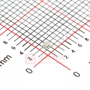
●Features 2 1) I C bus Interface ( f / s Mode Support, Slave Address : "0100011" ) 2) Spectral responsibility is approximately human eye response 3) Illuminance to Digital Converter 4) Wide range and High resolution. (1 – 65528 lx ) 5) Low Current by power down function 6) 50Hz / 60Hz Light noise reject-function 7) 1.8V Logic input interface 8) No need any external parts 9) Light source dependency is little. (ex. Incandescent Lamp. Fluorescent Lamp. Halogen Lamp. White LED. Sun Light) 10) Small measurement variation (+/- 15%) 11) Compact surface mount package 1.6 x 1.6 x 0.55 mm
●Applications Mobile phone, LCD TV, NOTE PC, Portable game machine, Digital camera, Digital video camera, Car navigation, PDA, LCD display
●Absolute Maximum Ratings Parameter Supply Voltage Operating Temperature Storage Temperature SDA Sink Current Power Dissipation
Symbol Vmax Topr Tstg Imax Pd
Limits 4.5 -40~85 -40~100 7 165※
Units V ℃ ℃ mA mW
※70mm × 70mm × 1.6mm glass epoxy board. Derating in done at 2.2mW/℃ for operating above Ta=25℃.
●Operating Conditions Parameter VCC Voltage I C Reference Voltage
2
Symbol Vcc VDVI
Min. 2.4 1.65
Typ. 3.0 -
Max. 3.6 VCC
Units V V
www.rohm.com © 2010 ROHM Co., Ltd. All rights reserved.
1/15
2010.02 - Rev.A
�BH1721FVC
●Electrical Characteristics ( VCC = 3.0V, DVI = 3.0V, Ta = 25℃, unless otherwise noted ) Parameter Supply Current Powerdown Current Peak Wave Length Measurement Accuracy Dark ( 0 lx ) Sensor out H-Resolution Mode Resolution L-Resolution Mode Resolution H-Resolution Mode Measurement Time L-Resolution Mode Measurement Time Incandescent / Fluorescent Sensor out ratio DVI Input ‘L’ Voltage SCL, SDA Input ‘H’ Voltage 1 SCL, SDA Input ‘H’ Voltage 2 SCL, SDA Input ‘L’ Voltage 1 SCL, SDA Input ‘L’ Voltage 2 SCL, SDA, Input ‘H’ Current SCL, SDA, Input ‘L’ Current I2C SCL Clock Frequency I2C Bus Free Time I2C Hold Time ( repeated ) START Condition I2C Set up time for a Repeated START Condition I2C Set up time for a Repeated STOP Condition I2C Data Hold Time I2C Data Valid Time I2C Data Valid Acknowledge Time I2C Data Setup Time I2C ‘L’ Period of the SCL Clock I2C ‘H’ Period of the SCL Clock I2C SDA Output ‘L’ Voltage Symbol Icc1 Icc2 λp S/A S0 rHR rLR tHR tLR rIF VDVL VIH1 VIH2 VIL1 VIL2 IIH IIL fSCL tBUF tHDSTA tSUSTA tSUSTO tHDDAT tVDDAT tVDACK tSUDAT tLOW tHIGH VOL Min. - - - 1.02 0 - - - - - - 0.7 * DVI 1.26 - - - - - 1.3 0.6 0.6 0.6 0 - - 100 1.3 0.6 0 Typ. 140 0.01 560 1.2 0 1 8 120 16 1 - - - - - - - - - - - - - - - - - - - Max. 199 1.0 - 1.38 2 - - 180 24 - 0.4 - - 0.3 * DVI DVI – 1.26 10 10 400 - - - - - 0.9 0.9 - - - 0.4
Technical Note
Units Conditions µA µA nm times Sensor out / Actual lx EV = 1000 lx ※1, ※2
※3
Ev = 100 lx
※1
No input Light
count H-Resolution Mode lx lx ms ms times EV = 1000 lx V V V V V µA µA kHz µs µs µs µs µs µs µs ns µs µs V IOL = 3 mA DVI ≧ 1.8V
1.65V ≦ DVI < 1.8V DVI ≧ 1.8V 1.65V ≦ DVI < 1.8V
※1 White LED is used as optical source. ※2 Measurement Accuracy typical value is possible to change '1' by "Measurement result adjustment function". ※3 Use H-Resolution Mode if dark data ( less than 20 lx ) is need.
www.rohm.com © 2010 ROHM Co., Ltd. All rights reserved.
2/15
2010.02 - Rev.A
�BH1721FVC
●Reference Data
1.2 1.0 0.8
Technical Note
64 56
100000
40 32 24 16 8
Measurement Result
32 40 48 56 64
Measurement Result
48
10000
Ratio
1000
0.6 0.4 0.2 0.0
400 500 600 700 800 900 1000 1100
H-Res. L-Res.
100
10
0
0 8 16
Wavelength [ nm ]
Illuminance [ lx ]
24
1
1 10 100 1000 10000 100000
Fig.1 Spectral Response
1.2 1
1.2 1
Fig.2 Illuminance Measurement Result 1
10
Fig.3 Illuminance Measuremnet Result 2
Illuminance [ lx ]
0.8
-
+
0.8
Measurement Result
1pin
Ratio
Ratio
8
+
0.6 0.4
6
0.6
-
1pin
0.2 0
-90 -60 -30 0
0.4
+
4
0.2 0
30 60 90
-90 -60 -30
+ +
2
H-Res.
0
60 90
-40 -20 0 20 40 60 80 100
0
30
Angle [ deg ]
Angle [ deg ]
Ta [ ℃ ]
Fig.4 Directional Characteristics 1
1.2 1 0.8
Fig.5 Directional Characteristics 2
200
Fig.6 Dark Response
Fluorescent Light Incandescent Light Halogen Light
ICC @ Measurement
150
Ratio
0.6
Kripton Light
100
0.4 0.2 0
-40 -20 0 20 40 60 80 100
Artifical Sun Light White LED
50
0
Ta [ ℃ ]
0 0.5
Ratio
1
1.5
2
2
2.5
3 VCC [ V ]
3.5
4
Fig.7 Measurement Result Temperature Dependency
10
Fig.8 Light Source Dependency (Fluorescent Light is set to ‘1’)
1.2
Fig.9 VCC – ICC (During measurement)
1.2 1
ICC @ POWER DOWN [ uA ]
1
DVI=1.8V
1
VCC=3V
0.8
0.8
Ratio
Ratio
0.6
0.6 0.4 0.2 0
0.1
0.4
0.2
0.01 -40 -20 0 20 40 60 80 100
0 2 2.5 3 3.5 4
1.5
2
2.5
3
3.5
Ta [ ℃ ]
VCC [ V ]
DVI [ V ]
Fig.10 VCC – ICC@0 lx (POWER DOWN)
Fig.11 Measurement Result VCC Dependency
Fig.12 Measurement Result DVI Dependency
www.rohm.com © 2010 ROHM Co., Ltd. All rights reserved.
3/15
2010.02 - Rev.A
�BH1721FVC
●Block Diagram VCC DVI
Technical Note
AMP
ADC
Logic + I C Interface
2
SCL SDA
PD OSC GND ●Block Diagram Descriptions ・PD Photo diode with approximately human eye response. ・AMP Integration-OPAMP for converting from PD current to Voltage. ・ADC AD converter for obtainment Digital 16bit data. 2 ・Logic + I C Interface Ambient Light Calculation and I2C BUS Interface. It is including below register. Data Register → This is for registration of Ambient Light Data. Initial Value is "0000_0000_0000_0000". Measurement Time Register → This is for registration of measurement time. Initial Value is "01_0010_1100". ・OSC Internal Oscillator. It is CLK for internal logic. ●Measurement Procedure
Power supply
Initial state is Power Down mode after VCC and DVI supply.
Power Down
Power On
Measurement command
State Transition by I2C write-command. Automatically State Transition Continuous measurement
* "Power On" Command is possible to omit.
www.rohm.com © 2010 ROHM Co., Ltd. All rights reserved.
4/15
2010.02 - Rev.A
�BH1721FVC
●Instruction Set Architecture Instruction Power Down Power On Continuously Auto-Resolution Mode Continuously H-Resolution Mode
Technical Note
Opecode 0000_0000 0000_0001 0001_0000 0010_0000 0001_0010 0010_0010 0001_0011 0001_0110 0010_0011 0010_0110 010_MT[9,8,7,6,5] 011_MT[4]_XXXX No active state.
Comments
Waiting for measurement command. Switch measurement mode automatically by illuminance. Start measurement at 1lx resolution. Measurement Time is typically 120ms. Start measurement at 8lx resolution. Measurement Time is typically 16ms. Change measurement time.
※ Please refer "adjust measurement result for influence of optical window."
Continuously L-Resolution Mode
Change Measurement time ( High bit ) Change Masurement time ( Low bit )
※ Don't input the other opecode.
Change measurement time.
※ Please refer "adjust measurement result for influence of optical window."
●Measurement mode explanation Measurement Mode Measurement Time. H-Resolution Mode L-Resolution Mode Typ. 120ms Typ. 16ms
Measurement Range. 0 - 8191 lx 0 - 65528 lx
Resolution 1 lx 8 lx
We recommend to use H-Resolution Mode. Measurement time (integration time) of H-Resolution Mode is so long that some kind of noise (including in 50Hz / 60Hz noise) is rejected. And H-Resolution Mode is 1 lx resolution so that it is suitable for darkness (less than 20 lx) Auto-Resolution mode selects measurement mode automatically. It is determined after 16ms (typ.) passes from measurement start. If BH1721FVC judges that current illuminance is more than 4000 lx, then Data is output at L-resolution mode, else Data is output after 120ms(typ.) from measurement start at H-resolution mode. Please refer below flow chart. Start
after 16ms.(typ.) Select mode Lux 4000
DATA output at L-resolution mode
Data output at H-resolution mode after 120ms passes from measurement start. Auto-Resolution mode measurement
www.rohm.com © 2010 ROHM Co., Ltd. All rights reserved.
5/15
2010.02 - Rev.A
�BH1721FVC
Technical Note
●Timing chart for VCC and DVI power supply sequence DVI is I2C bus reference voltage terminal. And it is also asynchronous reset terminal. It is necessary to set to ‘L’ after VCC is supplied. In DVI 'L' term, internal state is set to Power Down mode. 1) Recommended Timing chart1 for VCC and DVI supply.
VCC
DVI
Reset Term (more than 1µs) 2) Timing chart2 for VCC and DVI supply. (If DVI rises within 1µs after VCC supply)
VCC
DVI Reset Term (more than 1µs) Don't care state
www.rohm.com © 2010 ROHM Co., Ltd. All rights reserved.
6/15
2010.02 - Rev.A
�BH1721FVC
●Measurement sequence example from "Write instruction" to "Read measurement result" ex1) Continuously Auto-resolution mode from Master to Slave from Slave to Master
Technical Note
① Send "Continuously Auto-resolution mode " instruction ST 0100011 0 Ack 00010000 Ack SP
② Wait to complete 1st
Auto-resolution mode measurement.( max. 180ms )
③ Read measurement result. ST 0100011 1 Ack High Byte [ 15:8 ] Ack
Low Byte [ 7:0 ]
Ack
SP
How to calculate when the data High Byte is "10000011" and Low Byte is "10010000" 15 9 8 7 4 ( 2 + 2 + 2 + 2 + 2 ) / 1.2 ≒ 28067 [ lx ] The result of continuously measurement mode is updated. ex2) Continuously L-resolution mode ① Send " Continuously L-resolution mode " instruction ST 0100011 0 Ack 00010011 Ack SP
② Wait to complete L-resolution mode measurement.( max. 24ms ) ③ Read measurement result ST 0100011 1 Ack High Byte [ 15:8 ] Ack
Low Byte [ 7:0 ]
Ack
SP
How to calculate when the data High Byte is "00000001" and Low Byte is "00010000" 8 4 ( 2 + 2 ) / 1.2 ≒ 227 [ lx ]
www.rohm.com © 2010 ROHM Co., Ltd. All rights reserved.
7/15
2010.02 - Rev.A
�BH1721FVC
Technical Note
●Application circuit example of DVI terminal The DVI terminal is an asynchronous reset terminal. Please note that there is a possibility that IC doesn't operate normally if the reset section is not installed after the start-up of VCC. (Please refer to the paragraph of "Timing chart for VCC and DVI power supply sequence”) The description concerning SDA and the terminal SCL is omitted in this application circuit example. Please design the 2 application the standard of the I C bus as it finishes being satisfactory. ex 1) The control signal line such as CPU is connected.
BH1721FVC VCC SCL 0.1µF GND 0 DVI SDA.1µF 0.1µF
Micro Controller
ex 2) Reset IC is used. 1, For Reset IC of the Push-Pull type
BH1721FVC 0.1µF VCC SCL GND 0 DVI SDA.1µF 0.1µF RESET
Reset IC( Push-Pull type )
2, For Reset IC of the Open drain output
BH1721FVC 0.1µF VCC SCL GND 0 DVI SDA.1µF 0.1µF 1k Ω RESET Reset IC( Open drain type )
ex 3) A different power supply is used.
BH1721FVC VCC SCL 0.1µF V1 GND 0 DVI SDA.1µF V2 0.1µF
※ Power supply of DVI must stand up later than power supply of VCC stand up, because it is necessary to secure reset section ( 1µs or more ).
www.rohm.com © 2010 ROHM Co., Ltd. All rights reserved.
8/15
2010.02 - Rev.A
�BH1721FVC
Technical Note
ex 4) LPF using CR is inserted between VCC and DVI. This method has the possibility that the Reset section of turning on the power supply can not satisfied. Cannot be satisfied. Please design the set considering the characteristic of the power supply enough.
BH1721FVC 0.1µF VCC SCL GND 0 DVI SDA.1µF C1 : 1µF R1 : 1kΩ
◆ Notes when CR is inserted between VCC and DVI
※Please note that there is a possibility that reset section ( 1µs ) can not be satisfied because the power supply is turned on when the rise time of VCC is slow ※When VCC is turned off, the DVI voltage becomes higher than VCC voltage but IC destruction is not occred if recommended constant ( R1 = 1kΩ, C1 = 1µF ) is used. ※Please note that there is a possibility that Reset section (1µsec) cannot be satisfied if wait time is not enough long after turning off VCC. (It is necessary to consider DVI voltage level after turning off VCC.)
t1
t2
VCC DVI 2.4V
0.4V 0V Reset Section: 1µs or more
* Please do the application design to secure Reset section 1µs or more after the reclosing of the power supply.
◆ Example of designing set when CR ( C = 1µF, R = 1kΩ ) is inserted between VCC and DVI with VCC=2.8V ①The rise time to 0→2.4V of VCC must use the power supply of 100µs or less. ②Please wait 25ms or more after VCC turn off ( VCC
很抱歉,暂时无法提供与“BH1721FVC”相匹配的价格&库存,您可以联系我们找货
免费人工找货- 国内价格
- 1+3.366
- 10+2.673
- 600+2.6329
- 1200+2.55391
- 3000+2.43898