Datasheet
Ambient Light Sensor IC Series
Digital 16bit Serial Output Type
Ambient Light Sensor IC
BH1730FVC
General Description
2
Key Specifications
■
■
■
■
■
■
BH1730FVC is a digital Ambient Light Sensor IC with I C
bus interface. This IC is most suitable for obtaining
ambient light data for adjusting LCD and backlight power
of TV and mobile phone. It is capable of detecting a very
wide range of illuminance.
Supply Voltage Range:
2
I C I/O Voltage:
Detection Range:
Current Consumption:
Power Down Current:
Operating Temperature Range:
2.4V to 3.6V
1.65V to VCC V
0.001 lx to 100k lx
150 µA (Typ)
0.85 µA (Typ)
-40°C to +85°C
Features
■
■
■
■
■
■
■
■
2
I C bus Interface
f/s Mode Support, Slave Address "0101001"
2 outputs with peak wavelengths of visible light and
infrared light respectively.
Illuminance to digital converter
Low current by power down function
50Hz / 60Hz light noise reject function
Light source dependency is small by the calculation
using 2 outputs. (e.g. Incandescent lamp, Fluorescent
lamp, Halogen lamp, White LED and Sun light)
Built-in interrupt function
Sensitivity adjustment function for compensation for
illuminance decrease by optical window
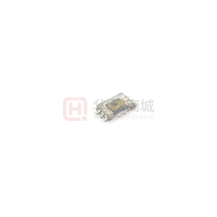
Package
W(Typ) x D(Typ) x H(Max)
1.60mm x 3.00mm x 0.75mm
WSOF6
WSOF6
Applications
LCD TV, Mobile Phone, Tablet PC, Note PC,
Digital Camera, Portable Game Machine
Typical Application Circuit
0.1uF
VCC
0.1uF
DVI
VDVI
AMP
ADC
PD for visible light
AMP
ADC
ADC Logic
+
2
I C Interface
+
INT Interface
SCL
SDA
INT
Micro
Controller
or
Baseband
Processor
PD for infrared light
OSC
POR
GND
○Product structure:Silicon monolithic integrated circuit.
○This product has no designed protection against radioactive rays.
○This product does not include laser transmitter.
○This product does not include optical load.
○This product includes Photo detector, ( Photo Diode ) inside of it.
.www.rohm.com
TSZ02201-0M3M0F616050-1-2
© 2012 ROHM Co., Ltd. All rights reserved.
1/20
8.Jun.2016 Rev.001
TSZ22111・14・001
�BH1730FVC
Pin Configuration
TOP VIEW
1
VCC
SCL 6
2
INT
DVI
3
GND
SDA 4
5
Pin Description
Pin No.
Pin Name
Function
1
VCC
2
INT
3
GND
Power supply terminal
INT pin output terminal.
If not in use, connect to GND or leave it open.
GND terminal
4
SDA
I C bus interface SDA terminal
5
DVI
I C bus I/O voltage
6
SCL
I C bus interface SCL terminal
2
2
2
Block Diagram
DVI
VCC
AMP
ADC
PD for visible light
AMP
ADC
SCL
ADC Logic
+
2
I C Interface
+
INT Interface
SDA
INT
PD for infrared light
OSC
POR
GND
Description of Blocks
1.
PD
Photo diodes (PD) with peak wavelengths of visible light and infrared light respectively.
2.
AMP
Integrating AMP for converting PD current to voltage.
3.
ADC
Analog-to-Digital Converter for obtaining 16bit digital data.
4.
ADC Logic + I C Interface + INT Interface
ADC control logic and I/F logic interface.
5.
OSC
Oscillator for clock of internal logic.
6.
POR
Power ON Reset. Please refer to "Power ON Sequence" on P14.
2
www.rohm.com
© 2012 ROHM Co., Ltd. All rights reserved.
TSZ22111・15・001
2/20
TSZ02201-0M3M0F616050-1-2
8.Jun.2016 Rev.001
�BH1730FVC
Absolute Maximum Ratings (Ta=25°C)
Parameter
Symbol
Rating
Unit
VCCMAX
4.5
V
VINTMAX, VSDAMAX,
VDVIMAX, VSCLMAX
-0.3 to +7
V
Operating Temperature
Topr
-40 to +85
°C
Storage Temperature
Tstg
-40 to +100
°C
SDA, INT Sink Current
IMAX
7
mA
Power Dissipation
Pd
Supply Voltage
INT, SDA, DVI, SCL Terminal Voltage
0.26
(Note 1)
W
(Note 1) 70mm x 70mm x 1.6mm glass epoxy board. Derating is at 3.47mW/°C for operating above Ta=25°C.
Caution: Operating the IC over the absolute maximum ratings may damage the IC. The damage can either be a short circuit between pins or an open circuit
between pins. Therefore, it is important to consider circuit protection measures, such as adding a fuse, in case the IC is operated over the absolute maximum
ratings.
Recommended Operating Conditions (Ta=-40℃ to +85℃)
Parameter
Supply Voltage
2
I C I/O Voltage
www.rohm.com
© 2012 ROHM Co., Ltd. All rights reserved.
TSZ22111・15・001
Symbol
Min
Typ
Max
Unit
VCC
2.4
3.0
3.6
V
VDVI
1.65
-
VCC
V
3/20
TSZ02201-0M3M0F616050-1-2
8.Jun.2016 Rev.001
�BH1730FVC
Electrical Characteristics (VCC = 3.0V, VDVI = 3.0V, Ta = 25°C, unless otherwise noted)
Parameter
Symbol
Min
Typ
Max
Unit
Conditions
(Note 1)
Supply Current
ICC1
-
150
200
µA
EV = 100 lx
CONTROL register(00h) = "03h"
and the other registers are default.
Power Down Current
ICC2
-
0.85
1.5
µA
No input Light
All registers are default.
Peak Wave Length of Type0
(Note 2)
λp0
-
600
-
nm
Peak Wave Length of Type1
(Note 2)
λp1
-
840
-
nm
(Note 1)
ADC Count Value of Type0
D1k_0
1020
1200
1380
count
EV = 1000 lx
TIMING register(01h) = "DAh"
GAIN register(07h) = "00h"
(Note 1)
ADC Count Value of Type1
D1k_1
153
180
207
count
Dark (0 lx) Sensor Out of Type0
S0_0
0
0
2
count
Dark (0 lx) Sensor Out of Type1
S0_1
0
0
2
count
EV = 1000 lx
TIMING register(01h) = "DAh"
GAIN register(07h) = "00h"
No input Light
TIMING register(01h) = "DAh"
GAIN register(07h) = "00h"
No input Light
TIMING register(01h) = "DAh"
GAIN register(07h) = “00h”
Gain x1 Resolution of Type0
(Note 2)
rG1
-
0.83
-
lx/count TIMING register(01h) = "DAh"
(Note 1)
Gain x2 Resolution of Type0
(Note 2)
rG2
-
0.42
-
lx/count TIMING register(01h) = "DAh"
(Note 1)
rG64
-
0.014
-
lx/count TIMING register(01h) = "DAh"
(Note 1)
rG128
-
0.007
-
lx/count TIMING register(01h) = "DAh"
(Note 1)
Tmt1
-
104.6
150
ms
Internal Clock Period
Tint
-
2.8
4.0
µs
INT Output 'L' Voltage
VINT
0
-
0.4
V
IINT = 3 mA
SCL, SDA Input 'H' Voltage 1
VIH1
0.7*VDVI
-
-
V
VDVI ≥ 1.8V
SCL, SDA Input 'H' Voltage 2
VIH2
1.26
-
-
V
1.65V ≤ VDVI 01h -> 02h -> 03h -> 04h -> 05h -> 06h -> 07h -> 12h -> 14h -> 15h -> 16h -> 17h
www.rohm.com
© 2012 ROHM Co., Ltd. All rights reserved.
TSZ22111・15・001
6/20
TSZ02201-0M3M0F616050-1-2
8.Jun.2016 Rev.001
�BH1730FVC
2. Measurement Procedure
Power
Supply
Initial state is power down mode after power supplied.
Power Down
POWER bit = H and
ADC_EN bit =H
Measurement
State transits after measurement time(Tmt).
Please refer to TIMING register on P9
about measurement time( Tmt ).
ONE_TIME bit = H?
Yes
No
INT_STOP bit = H and
INT is active?
Yes
No
2
State Transition by I C write-command.
Automatic State Transition
3. Software Reset Command.
All registers are reset and BH1730FVC becomes power down state by software reset command.
www.rohm.com
© 2012 ROHM Co., Ltd. All rights reserved.
TSZ22111・15・001
7/20
TSZ02201-0M3M0F616050-1-2
8.Jun.2016 Rev.001
�BH1730FVC
4. Command Set
Address
Type
[4:0]
-W
00h
RW
01h
RW
02h
RW
03h
RW
04h
RW
05h
RW
06h
RW
07h
RW
12h
R
14h
R
15h
R
16h
R
17h
R
Register name
Register function
COMMAND
CONTROL
TIMING
INTERRUPT
THLLOW
THLHIGH
THHLOW
THHHIGH
GAIN
ID
DATA0LOW
DATA0HIGH
DATA1LOW
DATA1HIGH
Specifies register address or sets special command
Operation mode control
Light integration time control
Interrupt function control
Low byte of low interrupt threshold setting
High byte of low interrupt threshold setting
Low byte of high interrupt threshold setting
High byte of high interrupt threshold setting
Gain control
Part number and Revision ID
ADC Type0 low byte data register
ADC Type0 high byte data register
ADC Type1 low byte data register
ADC Type1 high byte data register
(Note) Do not send command to the register which is not defined above.
(1) COMMAND
7
CMD
6
5
TRANSACTION
4
3
2
1
ADDRESS / Special command
0
default value 00h
Field
CMD
TRANSACTION
Bit
7
Type
W
6:5
W
Description
Write 1
00 : COMMAND is ADDRESS field.
01 : Reserved.
10 : Reserved.
11 : COMMAND is Special command field.
Specify register address.
Don’t specify invalid register address.
ADDRESS
4:0
W
Special command
www.rohm.com
© 2012 ROHM Co., Ltd. All rights reserved.
TSZ22111・15・001
00001 : Interrupt output reset.
00010 : Stop measurement in manual integration mode.
00011 : Start measurement in manual integration mode.
00100 : Software reset
Don’t input other commands.
8/20
TSZ02201-0M3M0F616050-1-2
8.Jun.2016 Rev.001
�BH1730FVC
(2) CONTROL (00h)
7
6
5
ADC_
INTR
RES
4
ADC_
VALID
3
ONE_
TIME
2
DATA_
SEL
1
ADC_
EN
0
POWER
default value 00h
Field
RES
Bit
7: 6
Type
RW
ADC_INTR
5
R
ADC_VALID
4
R
ONE_TIME
3
RW
DATA_SEL
2
RW
ADC_EN
1
RW
POWER
0
RW
(3) TIMING (01h)
7
6
5
Description
Write 00
0 : Interrupt is inactive.
1 : Interrupt is active.
0 : ADC data is not updated after last reading.
1 : ADC data is updated after last reading.
0 : ADC measurement is continuous.
1 : ADC measurement is one time.
ADC transits to power down automatically.
0 : ADC measurement Type0 and Type1.
1 : ADC measurement Type0 only.
0 : ADC measurement stops.
1 : ADC measurement starts.
0 : ADC power down.
1 : ADC power on.
4
3
2
1
0
ITIME
default value DAh
Field
Bit
Type
ITIME
7:0
RW
Description
00h
: Start / Stop of measurement is set by
special command.
(ADC manual integration mode)
01h to FFh : Integration time is determined by ITIME value
Integration Time : ITIME_ms = Tint * 964 * (256 - ITIME)
Measurement time : Tmt = ITIME_ms + Tint * 714
www.rohm.com
© 2012 ROHM Co., Ltd. All rights reserved.
TSZ22111・15・001
9/20
TSZ02201-0M3M0F616050-1-2
8.Jun.2016 Rev.001
�BH1730FVC
(4) INTERRUPT (02h)
7
6
INT_
RES
STOP
5
RES
4
INT_
EN
3
2
1
0
PERSIST
default value 00h
Field
RES
Bit
7
Type
RW
INT_STOP
6
RW
RES
5
RW
INT_EN
4
RW
3:0
RW
PERSIST
Description
Write 0
0 : ADC measurement does not stop.
1 : ADC measurement stops and transits to
power down mode when interrupt becomes active.
Write 0
0 : Disable interrupt function.
1 : Enable interrupt function.
Interrupt persistence function.
0000 : Interrupt becomes active at each measurement end.
0001 : Interrupt status is updated at each measurement end.
0010 : Interrupt status is updated if two consecutive threshold
judgments are the same.
When set 0011 or more, interrupt status is updated if same
threshold judgments continue consecutively same times as the
number set in “PERSIST”.
(5) TH_LOW (03h,04h)
Register
TH lower LSBs
TH lower MSBs
Address
03h
04h
Bit
7:0
7:0
Type
RW
RW
Description
Lower byte of low interrupt threshold
Upper byte of low interrupt threshold
default value 00h
(6) TH_UP (05h,06h)
Register
TH upper LSBs
TH upper MSBs
Address
05h
06h
Bit
7:0
7:0
Type
RW
RW
Description
Lower byte of high interrupt threshold
Upper byte of high interrupt threshold
default value FFh
4
3
(7) GAIN (07h)
7
6
5
RES
2
1
GAIN
0
default value 00h
Field
RES
Bit
7:3
Type
RW
GAIN
2:0
RW
www.rohm.com
© 2012 ROHM Co., Ltd. All rights reserved.
TSZ22111・15・001
Description
Write 00000
ADC resolution setting
X00 : x1 gain mode
X01 : x2 gain mode
X10 : x64 gain mode
X11 : x128 gain mode
10/20
TSZ02201-0M3M0F616050-1-2
8.Jun.2016 Rev.001
�BH1730FVC
(8) PART_ID ( 12h )
7
6
5
Part Number
4
3
2
1
Revision ID
0
default value 7Xh
Field
Part number
Revision ID
Bit
7:4
3:0
Type
R
R
Description
0111
Don’t use Revision ID Data
(9) DATA0 (14h,15h)
Register
DATA0 LSBs
DATA0 MSBs
Address
14h
15h
Bit
7:0
7:0
Type
R
R
Description
Lower byte of ADC Type0 data
Upper byte of ADC Type0 data
default value 00h
(10) DATA1 (16h,17h)
Register
DATA1 LSBs
DATA1 MSBs
Address
16h
17h
Bit
7:0
7:0
Type
R
R
Description
Lower byte of ADC Type1 data
Upper byte of ADC Type1 data
default value 00h
www.rohm.com
© 2012 ROHM Co., Ltd. All rights reserved.
TSZ22111・15・001
11/20
TSZ02201-0M3M0F616050-1-2
8.Jun.2016 Rev.001
�BH1730FVC
5. Measurement Sequence Example from "Write start measurement command" to "Read measurement result"
from Slave to Master
from Master to Slave
(1) Send "Continuous measurement mode" command.
Slave Address
W
ST
0101001
0
ACK
Write Command Register
1000_0000
ACK
Write CONTROL register
0000_0011
ACK
SP
SP
(2) Wait measurement completion.
(3) Read measurement result.
Slave Address
ST
0101001
W
0
ACK
Write Command Register
1001_0100
ACK
Slave Address
0101001
R
1
ACK
Read DATA0 LSBs register
ACK
ACK
Read DATA1 LSBs register
ACK
Read DATA1 MSBs register
NACK
ST
Read DATA0 MSBs register
www.rohm.com
© 2012 ROHM Co., Ltd. All rights reserved.
TSZ22111・15・001
12/20
SP
TSZ02201-0M3M0F616050-1-2
8.Jun.2016 Rev.001
�BH1730FVC
6. Lux Calculation using DATA0 and DATA1
BH1730FVC has two outputs, DATA0 (14h, 15h) for detecting mainly visible light, and DATA1 (16h, 17h) for detecting
mainly infrared light. Lux value can be calculated by using these two outputs. The calculation formula depends on the
characteristic of optical window. The example of the calculation is shown as below.
Ex) No optical window or optical window that has flat transmittance from visible light to infrared light.
i f ( D ATA 1 / D ATA 0 < 0 . 2 6 )
L x = ( 1 . 2 9 0 x D ATA 0 - 2 . 7 3 3 x D ATA 1 ) / G a i n x 1 0 2 . 6
e l s e i f ( D ATA 1 / D ATA 0 < 0 . 5 5 ) L x = ( 0 . 7 9 5 x D ATA 0 - 0 . 8 5 9 x D ATA 1 ) / G a i n x 1 0 2 . 6
e l s e i f ( D ATA 1 / D ATA 0 < 1 . 0 9 ) L x = ( 0 . 5 1 0 x D ATA 0 - 0 . 3 4 5 x D ATA 1 ) / G a i n x 1 0 2 . 6
e l s e i f ( D ATA 1 / D ATA 0 < 2 . 1 3 ) L x = ( 0 . 2 7 6 x D ATA 0 - 0 . 1 3 0 x D ATA 1 ) / G a i n x 1 0 2 . 6
else
L x= 0
/
/
/
/
I T I ME _ m s
I T I ME _ m s
I T I ME _ m s
I T I ME _ m s
ITIME_ms : Integration time of measurement (unit: ms). Please refer to TIMING register on P9.
7. Interrupt Function
Interrupt function compares measurement result to preset interrupt threshold level. BH1730FVC uses two threshold levels
(upper and lower). If measurement result is outside of the two thresholds, INT pin outputs 'L'. Interrupt threshold is set in
Interrupt threshold registers (03h - 06h).
Interrupt function is controlled by the Interrupt operational code. Interrupt persistence is set by PERSIST bit in
INTERRUPT register(02h).
INT pin is an Nch open drain terminal. Hence this terminal has to have an external pull-up resistor to a voltage source.
Maximum sink current rating of this terminal is 7mA.
INT terminal state is high impedance when VCC is supplied.
INT terminal becomes inactive by setting "Interrupt output reset" of special command. VCC current is consumed when
INT terminal is 'L'. So it is recommended to reset INT terminal immediately when interrupt is detected.
Master sends "Interrupt output reset" command.
INT Terminal
H
persistence = 1
L
H
persistence = 2
L
DATA0
Interrupt threshold H level
sequential measurement results
Interrupt threshold L level
time
www.rohm.com
© 2012 ROHM Co., Ltd. All rights reserved.
TSZ22111・15・001
13/20
TSZ02201-0M3M0F616050-1-2
8.Jun.2016 Rev.001
�BH1730FVC
8. Power On Sequence
ALL registers of BH1730FVC are reset when VCC powers up. There are some notes about power up and down sequence
as shown below.
(1) Power ON Time: t1
More than 2ms is needed to activate BH1730FVC after VCC becomes more than 2.4V from less than 0.4V.
Operating voltage is from 2.4V to 3.6V.
(2) Power OFF time: t2
More than 1ms (VCC < 0.4V) is needed before supplying power to BH1730FVC.
2.4V
VCC
0.4V
t1
t1
t2
BH1730FVC
Undefined Behavior
active
Undefined Behavior
active
Note: ”active state” means that BH1730FVC operates and accept I2C bus access correctly.
9.
ALS Sensitivity Adjustment Function
BH1730FVC is capable of changing its ALS sensitivity. This is used to compensate the effect of attenuation by the optical
window. Adjustment is done by changing the integration time. For example, when transmission rate of optical window is
1/n (measurement result becomes 1/n times if optical window is above the sensor), the effect of optical window is
compensated by changing integration time from default to n times.
Take note that at 100,000 lx or higher illuminance cannot be measured even when the sensitivity is decreased.
10. Optical Design for the Device
0.8 mm
1.3 mm
0.4mm
0.4mm
PD area
(0.25mm x 0.3 mm)
Please design the optical window so that light can
cover at least this are.
0.4mm 0.4mm
www.rohm.com
© 2012 ROHM Co., Ltd. All rights reserved.
TSZ22111・15・001
14/20
TSZ02201-0M3M0F616050-1-2
8.Jun.2016 Rev.001
�BH1730FVC
I/O Equivalent Circuit
PIN No.
Terminal Name
1
VCC
2
INT
3
GND
Equivalent Circuit
DVI
4
SDA
5
DVI
150kΩ
DVI
6
SCL
(Note) These values are typical value.
www.rohm.com
© 2012 ROHM Co., Ltd. All rights reserved.
TSZ22111・15・001
15/20
TSZ02201-0M3M0F616050-1-2
8.Jun.2016 Rev.001
�BH1730FVC
Operational Notes
1.
Reverse Connection of Power Supply
Connecting the power supply in reverse polarity can damage the IC. Take precautions against reverse polarity when
connecting the power supply, such as mounting an external diode between the power supply and the IC’s power
supply pins.
2.
Power Supply Lines
Design the PCB layout pattern to provide low impedance supply lines. Furthermore, connect a capacitor to ground at
all power supply pins. Consider the effect of temperature and aging on the capacitance value when using electrolytic
capacitors.
3.
Ground Voltage
Ensure that no pins are at a voltage below that of the ground pin at any time, even during transient condition.
4.
Ground Wiring Pattern
When using both small-signal and large-current ground traces, the two ground traces should be routed separately but
connected to a single ground at the reference point of the application board to avoid fluctuations in the small-signal
ground caused by large currents. Also ensure that the ground traces of external components do not cause variations
on the ground voltage. The ground lines must be as short and thick as possible to reduce line impedance.
5.
Thermal Consideration
Should by any chance the power dissipation rating be exceeded the rise in temperature of the chip may result in
deterioration of the properties of the chip. In case of exceeding this absolute maximum rating, increase the board size
and copper area to prevent exceeding the Pd rating.
6.
Recommended Operating Conditions
These conditions represent a range within which the expected characteristics of the IC can be approximately obtained.
The electrical characteristics are guaranteed under the conditions of each parameter.
7.
Inrush Current
When power is first supplied to the IC, it is possible that the internal logic may be unstable and inrush current may flow
instantaneously due to the internal powering sequence and delays, especially if the IC has more than one power
supply. Therefore, give special consideration to power coupling capacitance, power wiring, width of ground wiring, and
routing of connections.
8.
Operation Under Strong Electromagnetic Field
Operating the IC in the presence of a strong electromagnetic field may cause the IC to malfunction.
9.
Testing on Application Boards
When testing the IC on an application board, connecting a capacitor directly to a low-impedance output pin may
subject the IC to stress. Always discharge capacitors completely after each process or step. The IC’s power supply
should always be turned off completely before connecting or removing it from the test setup during the inspection
process. To prevent damage from static discharge, ground the IC during assembly and use similar precautions during
transport and storage.
10. Inter-pin Short and Mounting Errors
Ensure that the direction and position are correct when mounting the IC on the PCB. Incorrect mounting may result in
damaging the IC. Avoid nearby pins being shorted to each other especially to ground, power supply and output pin.
Inter-pin shorts could be due to many reasons such as metal particles, water droplets (in very humid environment) and
unintentional solder bridge deposited in between pins during assembly to name a few.
11. Unused Input Pins
Input pins of an IC are often connected to the gate of a MOS transistor. The gate has extremely high impedance and
extremely low capacitance. If left unconnected, the electric field from the outside can easily charge it. The small
charge acquired in this way is enough to produce a significant effect on the conduction through the transistor and
cause unexpected operation of the IC. So unless otherwise specified, unused input pins should be connected to the
power supply or ground line.
www.rohm.com
© 2012 ROHM Co., Ltd. All rights reserved.
TSZ22111・15・001
16/20
TSZ02201-0M3M0F616050-1-2
8.Jun.2016 Rev.001
�BH1730FVC
Operational Notes – continued
12. Regarding the Input Pin of the IC
This monolithic IC contains P+ isolation and P substrate layers between adjacent elements in order to keep them
isolated. P-N junctions are formed at the intersection of the P layers with the N layers of other elements, creating a
parasitic diode or transistor. For example (refer to figure below):
When GND > Pin A and GND > Pin B, the P-N junction operates as a parasitic diode.
When GND > Pin B, the P-N junction operates as a parasitic transistor.
Parasitic diodes inevitably occur in the structure of the IC. The operation of parasitic diodes can result in mutual
interference among circuits, operational faults, or physical damage. Therefore, conditions that cause these diodes to
operate, such as applying a voltage lower than the GND voltage to an input pin (and thus to the P substrate) should be
avoided.
Resistor
Transistor (NPN)
Pin A
Pin B
C
E
Pin A
N
P+
P
N
N
P+
N
Pin B
B
Parasitic
Elements
N
P+
N P
N
P+
B
N
C
E
Parasitic
Elements
P Substrate
P Substrate
GND
GND
Parasitic
Elements
GND
Parasitic
Elements
GND
N Region
close-by
Figure 3. Example of monolithic IC structure
13. Ceramic Capacitor
When using a ceramic capacitor, determine the dielectric constant considering the change of capacitance with
temperature and the decrease in nominal capacitance due to DC bias and others.
14. Area of Safe Operation (ASO)
Operate the IC such that the output voltage, output current, and power dissipation are all within the Area of Safe
Operation (ASO).
www.rohm.com
© 2012 ROHM Co., Ltd. All rights reserved.
TSZ22111・15・001
17/20
TSZ02201-0M3M0F616050-1-2
8.Jun.2016 Rev.001
�BH1730FVC
Ordering Information
B
H
1
7
3
0
Part Number
F
V
C
-
Package
FVC: WSOF6
TR
Packaging and forming specification
TR: Embossed tape and reel
Marking Diagram and Methods of Distinguishing 1pin
There are some methods to distinguish 1pin.
① Distinguishing by 1Pin marking
② Distinguishing by die pattern
③ Distinguishing by taper part of 1-3pin side
②(by die pattern) is the easiest method to distinguish by naked eye.
②
A
H
LOT Number
③
Part Number Marking
①
www.rohm.com
© 2012 ROHM Co., Ltd. All rights reserved.
TSZ22111・15・001
18/20
TSZ02201-0M3M0F616050-1-2
8.Jun.2016 Rev.001
�BH1730FVC
Physical Dimension, Tape and Reel Information
Package Name
www.rohm.com
© 2012 ROHM Co., Ltd. All rights reserved.
TSZ22111・15・001
WSOF6
19/20
TSZ02201-0M3M0F616050-1-2
8.Jun.2016 Rev.001
�BH1730FVC
Revision History
Date
8. Jun. 2016
Revision
001
Changes
New release
www.rohm.com
© 2012 ROHM Co., Ltd. All rights reserved.
TSZ22111・15・001
20/20
TSZ02201-0M3M0F616050-1-2
8.Jun.2016 Rev.001
�Notice
Precaution on using ROHM Products
1.
Our Products are designed and manufactured for application in ordinary electronic equipments (such as AV equipment,
OA equipment, telecommunication equipment, home electronic appliances, amusement equipment, etc.). If you
(Note 1)
intend to use our Products in devices requiring extremely high reliability (such as medical equipment
, transport
equipment, traffic equipment, aircraft/spacecraft, nuclear power controllers, fuel controllers, car equipment including car
accessories, safety devices, etc.) and whose malfunction or failure may cause loss of human life, bodily injury or
serious damage to property (“Specific Applications”), please consult with the ROHM sales representative in advance.
Unless otherwise agreed in writing by ROHM in advance, ROHM shall not be in any way responsible or liable for any
damages, expenses or losses incurred by you or third parties arising from the use of any ROHM’s Products for Specific
Applications.
(Note1) Medical Equipment Classification of the Specific Applications
JAPAN
USA
EU
CHINA
CLASSⅢ
CLASSⅡb
CLASSⅢ
CLASSⅢ
CLASSⅣ
CLASSⅢ
2.
ROHM designs and manufactures its Products subject to strict quality control system. However, semiconductor
products can fail or malfunction at a certain rate. Please be sure to implement, at your own responsibilities, adequate
safety measures including but not limited to fail-safe design against the physical injury, damage to any property, which
a failure or malfunction of our Products may cause. The following are examples of safety measures:
[a] Installation of protection circuits or other protective devices to improve system safety
[b] Installation of redundant circuits to reduce the impact of single or multiple circuit failure
3.
Our Products are designed and manufactured for use under standard conditions and not under any special or
extraordinary environments or conditions, as exemplified below. Accordingly, ROHM shall not be in any way
responsible or liable for any damages, expenses or losses arising from the use of any ROHM’s Products under any
special or extraordinary environments or conditions. If you intend to use our Products under any special or
extraordinary environments or conditions (as exemplified below), your independent verification and confirmation of
product performance, reliability, etc, prior to use, must be necessary:
[a] Use of our Products in any types of liquid, including water, oils, chemicals, and organic solvents
[b] Use of our Products outdoors or in places where the Products are exposed to direct sunlight or dust
[c] Use of our Products in places where the Products are exposed to sea wind or corrosive gases, including Cl2,
H2S, NH3, SO2, and NO2
[d] Use of our Products in places where the Products are exposed to static electricity or electromagnetic waves
[e] Use of our Products in proximity to heat-producing components, plastic cords, or other flammable items
[f] Sealing or coating our Products with resin or other coating materials
[g] Use of our Products without cleaning residue of flux (even if you use no-clean type fluxes, cleaning residue of
flux is recommended); or Washing our Products by using water or water-soluble cleaning agents for cleaning
residue after soldering
[h] Use of the Products in places subject to dew condensation
4.
The Products are not subject to radiation-proof design.
5.
Please verify and confirm characteristics of the final or mounted products in using the Products.
6.
In particular, if a transient load (a large amount of load applied in a short period of time, such as pulse. is applied,
confirmation of performance characteristics after on-board mounting is strongly recommended. Avoid applying power
exceeding normal rated power; exceeding the power rating under steady-state loading condition may negatively affect
product performance and reliability.
7.
De-rate Power Dissipation depending on ambient temperature. When used in sealed area, confirm that it is the use in
the range that does not exceed the maximum junction temperature.
8.
Confirm that operation temperature is within the specified range described in the product specification.
9.
ROHM shall not be in any way responsible or liable for failure induced under deviant condition from what is defined in
this document.
Precaution for Mounting / Circuit board design
1.
When a highly active halogenous (chlorine, bromine, etc.) flux is used, the residue of flux may negatively affect product
performance and reliability.
2.
In principle, the reflow soldering method must be used on a surface-mount products, the flow soldering method must
be used on a through hole mount products. If the flow soldering method is preferred on a surface-mount products,
please consult with the ROHM representative in advance.
For details, please refer to ROHM Mounting specification
Notice-PGA-E
© 2015 ROHM Co., Ltd. All rights reserved.
Rev.003
�Precautions Regarding Application Examples and External Circuits
1.
If change is made to the constant of an external circuit, please allow a sufficient margin considering variations of the
characteristics of the Products and external components, including transient characteristics, as well as static
characteristics.
2.
You agree that application notes, reference designs, and associated data and information contained in this document
are presented only as guidance for Products use. Therefore, in case you use such information, you are solely
responsible for it and you must exercise your own independent verification and judgment in the use of such information
contained in this document. ROHM shall not be in any way responsible or liable for any damages, expenses or losses
incurred by you or third parties arising from the use of such information.
Precaution for Electrostatic
This Product is electrostatic sensitive product, which may be damaged due to electrostatic discharge. Please take proper
caution in your manufacturing process and storage so that voltage exceeding the Products maximum rating will not be
applied to Products. Please take special care under dry condition (e.g. Grounding of human body / equipment / solder iron,
isolation from charged objects, setting of Ionizer, friction prevention and temperature / humidity control).
Precaution for Storage / Transportation
1.
Product performance and soldered connections may deteriorate if the Products are stored in the places where:
[a] the Products are exposed to sea winds or corrosive gases, including Cl2, H2S, NH3, SO2, and NO2
[b] the temperature or humidity exceeds those recommended by ROHM
[c] the Products are exposed to direct sunshine or condensation
[d] the Products are exposed to high Electrostatic
2.
Even under ROHM recommended storage condition, solderability of products out of recommended storage time period
may be degraded. It is strongly recommended to confirm solderability before using Products of which storage time is
exceeding the recommended storage time period.
3.
Store / transport cartons in the correct direction, which is indicated on a carton with a symbol. Otherwise bent leads
may occur due to excessive stress applied when dropping of a carton.
4.
Use Products within the specified time after opening a humidity barrier bag. Baking is required before using Products of
which storage time is exceeding the recommended storage time period.
Precaution for Product Label
A two-dimensional barcode printed on ROHM Products label is for ROHM’s internal use only.
Precaution for Disposition
When disposing Products please dispose them properly using an authorized industry waste company.
Precaution for Foreign Exchange and Foreign Trade act
Since concerned goods might be fallen under listed items of export control prescribed by Foreign exchange and Foreign
trade act, please consult with ROHM in case of export.
Precaution Regarding Intellectual Property Rights
1.
All information and data including but not limited to application example contained in this document is for reference
only. ROHM does not warrant that foregoing information or data will not infringe any intellectual property rights or any
other rights of any third party regarding such information or data.
2.
ROHM shall not have any obligations where the claims, actions or demands arising from the combination of the
Products with other articles such as components, circuits, systems or external equipment (including software).
3.
No license, expressly or implied, is granted hereby under any intellectual property rights or other rights of ROHM or any
third parties with respect to the Products or the information contained in this document. Provided, however, that ROHM
will not assert its intellectual property rights or other rights against you or your customers to the extent necessary to
manufacture or sell products containing the Products, subject to the terms and conditions herein.
Other Precaution
1.
This document may not be reprinted or reproduced, in whole or in part, without prior written consent of ROHM.
2.
The Products may not be disassembled, converted, modified, reproduced or otherwise changed without prior written
consent of ROHM.
3.
In no event shall you use in any way whatsoever the Products and the related technical information contained in the
Products or this document for any military purposes, including but not limited to, the development of mass-destruction
weapons.
4.
The proper names of companies or products described in this document are trademarks or registered trademarks of
ROHM, its affiliated companies or third parties.
Notice-PGA-E
© 2015 ROHM Co., Ltd. All rights reserved.
Rev.003
�Datasheet
General Precaution
1. Before you use our Pro ducts, you are requested to care fully read this document and fully understand its contents.
ROHM shall n ot be in an y way responsible or liabl e for fa ilure, malfunction or acci dent arising from the use of a ny
ROHM’s Products against warning, caution or note contained in this document.
2. All information contained in this docume nt is current as of the issuing date and subj ect to change without any prior
notice. Before purchasing or using ROHM’s Products, please confirm the la test information with a ROHM sale s
representative.
3.
The information contained in this doc ument is provi ded on an “as is” basis and ROHM does not warrant that all
information contained in this document is accurate an d/or error-free. ROHM shall not be in an y way responsible or
liable for an y damages, expenses or losses incurred b y you or third parties resulting from inaccur acy or errors of or
concerning such information.
Notice – WE
© 2015 ROHM Co., Ltd. All rights reserved.
Rev.001
�


 工商网监
湘ICP备2023018690号
工商网监
湘ICP备2023018690号

