Datasheet
Pressure Sensor series
Pressure Sensor IC
BM1386GLV
General Description
Key Specifications
BM1386GLV is piezo-resistive pressure sensor.
BM1386GLV performs temperature compensation for
MEMS inside chip internally, so it’s very easy to get
pressure information.
Features
Pressure Range:
300hPa to 1300hPa
Relative Pressure Accuracy:
±0.12hPa(Typ)
Absolute Pressure Accuracy:
±1hPa(Typ)
Operating Temperature Range:
-40°C to +85°C
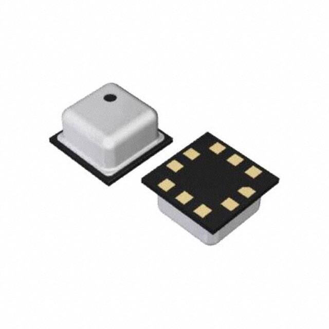
Package
Piezo-resistive pressure sensor
Pressure range is from 300hPa to 1300hPa
Built-in temperature compensation
function.
I2C bus interface (f/s mode support)
Built-in FIFO
Small package
W(Typ) x D(Typ) x H(Max)
2.0mm x 2.0mm x 1.0mm
CLGA10V020A
Applications
Smartphone, Healthcare, mobile device (e.g. game).
Typical Application Circuit
BM1386GLV
Regulator
(internal)
VREG
VDD
Memory
VSS
TEST3
Pressure Sensor
Mux
ADC
signal
processing
I2 C
SDA
SCL
TEST2
HOST
DRI
Temperature
Sensor
Clock
TEST1
TEST0
〇Product structure : Silicon monolithic integrated circuit
.www.rohm.com
© 2017 ROHM Co., Ltd. All rights reserved.
TSZ22111 • 14 • 001
〇This product has no designed protection against radioactive rays
1/29
TSZ02201-0M1M0FZ17010-1-2
14.Nov.2017 Rev.002
�BM1386GLV
Contents
General Description ........................................................................................................................................................................ 1
Features.......................................................................................................................................................................................... 1
Applications .................................................................................................................................................................................... 1
Key Specifications .......................................................................................................................................................................... 1
Package .......................................................................................................................................................................................... 1
Typical Application Circuit ............................................................................................................................................................... 1
Pin Configuration ............................................................................................................................................................................ 3
Pin Description................................................................................................................................................................................ 3
Block Diagram ................................................................................................................................................................................ 4
Absolute Maximum Ratings .......................................................................................................................................................... 5
Thermal Resistance ........................................................................................................................................................................ 5
Recommended Operating Conditions ........................................................................................................................................... 5
Electrical Characteristics ............................................................................................................................................................... 6
I2C Bus Timing Characteristics ..................................................................................................................................................... 7
I2C Bus Communication .................................................................................................................................................................. 7
I2C bus Slave Address .................................................................................................................................................................... 8
Register Map .................................................................................................................................................................................. 8
FIFO ............................................................................................................................................................................................. 14
Interrupt function ........................................................................................................................................................................... 16
Typical Performance Curves......................................................................................................................................................... 17
Control sequence.......................................................................................................................................................................... 18
Application Example ..................................................................................................................................................................... 23
I/O Equivalent Circuits .................................................................................................................................................................. 24
Operational Notes ......................................................................................................................................................................... 25
Ordering Information ..................................................................................................................................................................... 27
Marking Diagrams ......................................................................................................................................................................... 27
Physical Dimension, Tape and Reel Information .......................................................................................................................... 28
Revision History ............................................................................................................................................................................ 29
www.rohm.co.jp
© 2017 ROHM Co., Ltd. All rights reserved.
TSZ22111 • 15 • 001
2/29
TSZ02201-0M1M0FZ17010-1-2
14.Nov.2017 Rev.002
�BM1386GLV
Pin Configuration
Top View
(pads not visible)
2
1
SCL
VREG
3
10
TEST0
VDD
4
9
SDA
VSS
5
8
TEST2
TEST1
6
7
TEST3
DRI
Pin Description
Pin No.
1
Pin Name
VREG
2
SCL
3
TEST0
Function
Internal power supply
pin(Note 1)
I2C serial bus colck pin
Test pin (connect to VSS)
4
SDA
5
TEST2
I2C serial bus data pin
Test pin (open)
6
TEST3
Test pin (connect to VDD)
7
DRI
Interrupt notice output pin
8
TEST1
Test pin (connect to VSS)
9
VSS
Ground pin
10
VDD
power voltage pin(Note 2)
(Note 1) Dispose a bypass capacitor as close as possible to the IC.
Please set a bypass capacitor of 0.22µF between DREG and VSS.
Please do not use this pin for external power source.
(Note 2) Dispose a bypass capacitor as close as possible to the IC.
www.rohm.co.jp
© 2017 ROHM Co., Ltd. All rights reserved.
TSZ22111 • 15 • 001
3/29
TSZ02201-0M1M0FZ17010-1-2
14.Nov.2017 Rev.002
�BM1386GLV
Block Diagram
BM1386GLV
Regulator
(internal)
VREG
VDD
Memory
VSS
TEST3
Pressure Sensor
SDA
Mux
ADC
signal
processing
Temperature
Sensor
I2 C
SCL
TEST2
DRI
Clock
TEST1
TEST0
www.rohm.co.jp
© 2017 ROHM Co., Ltd. All rights reserved.
TSZ22111 • 15 • 001
4/29
TSZ02201-0M1M0FZ17010-1-2
14.Nov.2017 Rev.002
�BM1386GLV
Absolute Maximum Ratings (Ta = 25°C)
Parameter
Power Supply
Symbol
Rating
Unit
VDD_MR
4.5
V
Input
Voltage1(Note 1)
VIN1MR
Input
VIN2MR
Tstg
-0.3 to +4.5
-0.3 to (VDD+0.3) or +4.5
whichever is less
-40 to +125
V
Voltage2(Note 2)
°C
Tjmax
125
°C
Povr
20000
hPa
Storage Temperature
Maximum Junction Temperature
Pressure
V
(Note 1) DRI, SCL, SDA pin
(Note 2) except DRI, SCL, SDA pin
Caution 1: Operating the IC over the absolute maximum ratings may damage the IC. The damage can either be a short circuit between pins or an open circuit
between pins and the internal circuitry. Therefore, it is important to consider circuit protection measures, such as adding a fuse, in case the IC is
operated over the absolute maximum ratings.
Caution 2: Should by any chance the maximum junction temperature rating be exceeded the rise in temperature of the chip may result in deterioration of the
properties of the chip. In case of exceeding this absolute maximum rating, increase the board size and copper area to prevent exceeding the
maximum junction temperature rating.
Thermal Resistance(Note 1)
Parameter
Symbol
Thermal Resistance (Typ)
Unit
1s(Note 3)
2s2p(Note 4)
θJA
339.7
217.5
°C/W
ΨJT
154
140
°C/W
CLGA10V020A
Junction to Ambient
Junction to Top Characterization
Parameter(Note 2)
(Note 1)Based on JESD51-2A(Still-Air)
(Note 2)The thermal characterization parameter to report the difference between junction temperature and the temperature at the top center of the outside
surface of the component package.
(Note 3)Using a PCB board based on JESD51-3.
Layer Number of
Measurement Board
Single
Material
Board Size
FR-4
114.3mm x 76.2mm x 1.57mmt
Top
Copper Pattern
Thickness
Footprints and Traces
70μm
(Note 4)Using a PCB board based on JESD51-7.
Layer Number of
Measurement Board
4 Layers
Material
Board Size
FR-4
114.3mm x 76.2mm x 1.6mmt
Top
2 Internal Layers
Bottom
Copper Pattern
Thickness
Copper Pattern
Thickness
Copper Pattern
Thickness
Footprints and Traces
70μm
74.2mm x 74.2mm
35μm
74.2mm x 74.2mm
70μm
Recommended Operating Conditions
Parameter
Power Supply
Input
I2 C
Voltage1(Note 1)
clock Input Frequency
Operating Temperature
Symbol
Min
Typ
Max
Unit
VDD
1.7
1.8
3.6
V
VIN1
0.0
-
3.6
V
fSCL
-
-
400
kHz
Topr
-40
+25
+85
°C
(Note 1) DRI, SCL, SDA pin
www.rohm.co.jp
© 2017 ROHM Co., Ltd. All rights reserved.
TSZ22111 • 15 • 001
5/29
TSZ02201-0M1M0FZ17010-1-2
14.Nov.2017 Rev.002
�BM1386GLV
Electrical Characteristics (Unless otherwise specified VDD=1.8V Ta=25°C)
Parameter
Symbol
Min
Typ
Max
Unit
Conditions
ISS
-
1
5
µA
L Input Voltage(Note 1)
VIL
-
-
0.3 *
VDD
V
H Input Voltage(Note 1)
VIH
-
-
V
L Input
Current(Note 1)
IIL
0.7 *
VDD
-10
-
-
μA
VIL = GND
H Input
Current(Note 1)
10
0.2 *
VDD
0.2 *
VDD
μA
VIH = VDD
V
IL = -0.3mA
V
IL = -3mA
Current Consumption
Power Down Mode Current
PWR_DOWN=0, RSTB=0
Logic
IIH
-
-
1(Note 2)
VOL1
-
-
L Output Voltage 2(Note 3)
VOL2
-
-
PR
300
-
1300
hPa
0°C to 65°C
L Output Voltage
Pressure characteristics
Pressure Detection Range
Accuracy(Note 4)
Prel
-
±0.12
-
hPa
950hPa to 1050hPa
Absolute Pressure Accuracy
Pabs
-
±1
-
hPa
1000hPa
Temperature Accuracy
Tabs
-
±2
-
°C
Tm
-
-
6
msec
Relative Pressure
Measurement
Time(Note 5)
25°C to 85°C
AVE_NUM=000
(Note 1) SDA, SCL pin
(Note 2) DRI pin
(Note 3) SDA pin
(Note 4) Target values
(Note 5) Measurement time is changed by average number of measurement data. It is written in Measurement time more detail.
www.rohm.co.jp
© 2017 ROHM Co., Ltd. All rights reserved.
TSZ22111 • 15 • 001
6/29
TSZ02201-0M1M0FZ17010-1-2
14.Nov.2017 Rev.002
�BM1386GLV
I2C Bus Timing Characteristics (Unless otherwise specified VDD=1.8V, Ta=25°C)
VIH
VIH
SDA
P : STOP
S : Repeated START
S : START
VIL
VIL
VIL
S : START
VIH
VIH
VIL
tBUF
tHD;STA
tSU;DAT
VIH
SCL
VIL
tLOW
tHD;STA
VIH
VIH
VIL
VIH
VIH
VIH
VIL
tHIGH
tHD;DAT
Parameter
tSU;STA
tSU;STO
Symbol
Min
Typ
Max
Unit
SCL Clock frequency
fSCL
0
-
400
kHz
‘L’ Period of the SCL Clock
tLOW
1.3
-
-
µs
‘H’ Period of the SCL Clock
tHIGH
0.6
-
-
µs
Setup Time for Repeated START
tSU;STA
0.6
-
-
µs
Hold Time for START
tHD;STA
0.6
-
-
µs
Data Setup Time
tSU;DAT
100
-
-
ns
Data Hold Time
tHD;DAT
0
-
-
µs
Setup Time for STOP
tSU;STO
0.6
-
-
µs
tBUF
1.3
-
-
µs
Bus Free Time between STOP and START
Conditions
I2C Bus Communication
1. Write Format
(1) Indicate register address
S
W
0
Slave Address
ACK
Register Address
ACK
ACK
Register Address
ACK
P
(2) Write data after indicating register address
S
W
0
Slave Address
Data specified at register
address field
ACK
・・・
ACK
Data specified at register
address field + N
ACK
P
NACK
P
NACK
P
2. Read Format
(1) Read data after indicating register address
S
Slave Address
W
0
ACK
S
Slave Address
R
1
ACK
Data specified at register
address field + 1
ACK
・・・
Register Address
ACK
Data specified at register
address field
ACK
ACK
Data specified at register
address field + N
(2) Read data from the specified register
S
Slave Address
Data specified at register
address field + 1
R
1
ACK
ACK
・・・
Data specified at register
address field
ACK
from master to slave
www.rohm.co.jp
© 2017 ROHM Co., Ltd. All rights reserved.
TSZ22111 • 15 • 001
ACK
Data specified at register
address field + N
from slave to master
7/29
TSZ02201-0M1M0FZ17010-1-2
14.Nov.2017 Rev.002
�BM1386GLV
I2C bus Slave Address
The slave address is “1011101”.
Register Map(Note 1)
Register
Address
Register Name
R/W
0x0F
MANUFACTURER ID
R
MANUFACTURER ID [7:0]
0x10
PART ID
R
PART ID [7:0]
0x12
POWER_DOWN
RW
0
0
0
0
0x13
RESET
RW
0
0
0
0x14
MODE_CONTROL
RW
0x15
IIR, FIFO
CONTROL
RW
FIFO_
EN
WTM_
LEVEL
0x18
FIFO data
R
0
0
0x19
STATUS
R
0
0
0x1A
0x1B
PRESSURE
0x1C
D6
D5
AVE_NUM[2:0]
0
D4
D3
D2
D1
D0
0
0
0
PWR_
DOWN
0
0
0
0
RSTB
DR_EN
FULL
_EN
WTM
_EN
MODE[1:0]
0
0
0
IIR_MODE[1:0]
FIFO_LEV[5:0]
0
0
0
R
PRESS_OUT[15:8]
R
PRESS_OUT[7:0]
R
0x1D
D7
PRESS_OUT_XL[5:0]
R
TEMP_OUT[15:8]
R
TEMP_OUT[7:0]
RD_
FULL
RD_
WTM
RD_
DRDY
0
0
TEMPERATURE
0x1E
(Note 1)Do not write any commands to other addresses except above. Do not write ‘1’ to the fields in which value is ‘0’ in above table.
Address from 0x14 to 0x1E registers can be accessed only when PWR_DOWN=1 and RSTB=1. (In other case Write: Ignored, Read: 0xXX)
www.rohm.co.jp
© 2017 ROHM Co., Ltd. All rights reserved.
TSZ22111 • 15 • 001
8/29
TSZ02201-0M1M0FZ17010-1-2
14.Nov.2017 Rev.002
�BM1386GLV
( 0x0F ) MANUFACTURER ID
Fields
MANUFACTURER ID [7:0]
Function
Manufacturer ID : 0xE0
( 0x10 ) PART ID
Fields
PART ID [7:0]
Function
Part ID : 0x33
( 0x12 ) POWER_DOWN
Fields
Function
0: power down
1: active
PWR_DOWN
default value 0x00
( 0x13 ) RESET
Fields
RSTB
Function
0: Measurement control block is reset
1: Measurement control block is active
default value 0x00
www.rohm.co.jp
© 2017 ROHM Co., Ltd. All rights reserved.
TSZ22111 • 15 • 001
9/29
TSZ02201-0M1M0FZ17010-1-2
14.Nov.2017 Rev.002
�BM1386GLV
( 0x14 ) MODE_CONTROL
Fields
Function
AVE_NUM[2:0]
Seting of the averaging number of measurement data
000: single, 001: 2 times, 010: 4 times,
011: 8 times, 100: 16 times, 101: 32 times,
110: 64 times, 111: Prohibited
DR_EN
DRI pin Enable for Data Ready
Details are written in Interrupt.
0 : DRI pin Disable, 1 : DRI pin Enable
FULL_EN
DRI pin Enable for FULL
Details are written in Interrupt.
0 : DRI pin Disable, 1 : DRI pin Enable
WTM_EN
DRI pin Enable for Water Mark
Details are written in Interrupt.
0 : DRI pin Disable, 1 : DRI pin Enable
MODE[1:0]
Measurement mode setting (Pressure and Temperature are measured at one rate)
00 : Stand by, 01 : One shot, 10 : Continuous, 11 : Prohibited
default value 0x00
Measurement time and RMS noise against number of average
Measurement
Measurement
RMS noise
AVE_NUM
time Tm
cycle Ti
[hPa]
max[ms]
max[ms]
000
6
60
0.090
001
9
60
0.063
010
16
60
0.045
011
30
60
0.032
100
60
60
0.023
101
120
120
0.016
110
240
240
0.011
RMS noise is calculated as standard deviation of 32 data points (1σ).
RMS noise is a reference value and it’s not the value with guarantee.
Condition VDD=1.8V, Ta=25°C, IIR_MODE=00
Measurement time
One shot mode perform one measurement. Measurement data is updated when measurement completed, so it
should be read more than Tm after measurement start.
Continuous mode repeat measurement in every measurement cycle Ti. The latest measurement data which is
completed is read.
Measurement time Tm and measurement cycle Ti is determined by number of average.
Pressure data of first time
measurement is read.
Measurement cycle Ti
Measurement time Tm
Measurement time Tm
Measurement
Start of
measurement
First Measurement
Measurement
Start of
measurement
Start of
measurement
www.rohm.co.jp
© 2017 ROHM Co., Ltd. All rights reserved.
TSZ22111 • 15 • 001
Second measurement
10/29
TSZ02201-0M1M0FZ17010-1-2
14.Nov.2017 Rev.002
�BM1386GLV
Operation mode transition
Please refer to the below figure of operation mode transition.
Power down mode is the smallest current consumption mode due to circuit is OFF. Please set this mode when
reducing current consumption. Measurement is not available in this mode, so the measurement is performed after
switching to standby mode.
In reset mode, regulator for internal blocks is active and measurement control block is reset. Register is initialized in
Reset mode. Measurement command is acceptable when “1” is written in “RSTB”
There are 2 measurement modes. One shot mode and Continuous mode. They are transferred from stand by mode.
Then, please set “AVE_NUM” register at the same time.
Please write “0x1400” when transferring to standby mode again.
In one shot mode, a single measurement is performed when “01” is written in “MODE”. After the measurement
completes, it is transferred to standby mode automatically. When “0x1400” is written before end of measurement,
mode is switched to standby immediately but pressure value is not updated.
Transition to the other measurement mode during measurement in one shot mode is forbidden.
In Continuous mode, when “10” is written in “MODE”, measurement starts and it continues until “0x1400” is written.
Transition to the other measurement mode from Continuous mode is forbidden.
Power Down
Regulator:OFF
Processing:OFF
0x1201
0x1200
Reset
Regulator:ON
Processing:OFF
0x1301
0x1400
0x1300
Stand by
Regulator:ON
Processing:ON
0x14X1
0x14X2
After measurement
time Tm
or
0x1400
One Shot
0x1400
Continuous
Prohibition
0x14X1
→ Prohibited
0x14X2
→ Prohibited
0xYYZZ (send command)
YY:Address
ZZ:Data
www.rohm.co.jp
© 2017 ROHM Co., Ltd. All rights reserved.
TSZ22111 • 15 • 001
11/29
TSZ02201-0M1M0FZ17010-1-2
14.Nov.2017 Rev.002
�BM1386GLV
( 0x15 ) IIR, FIFO CONTROL
Fields
Function
FIFO_EN
FIFO mode setting
Details are written in FIFO.
0: Bypass mode, 1: FIFO mode
WTM_LEVEL
Water Mark level setting
Details are written in FIFO.
0: Water Mark interrupt occur when FIFO memory is 24 or above.
1: Water Mark interrupt occur when FIFO memory is 28 or above.
IIR_MODE[1:0]
IIR filter enable and coefficient setting
00 : IIR OFF, 01 : IIR ON (weak)
10 : IIR ON (middle), 11 : IIR ON (strong)
default value 0x00
( 0x18 ) FIFO data
Fields
Function
FIFO_LEV[5:0]
Number of sample in FIFO
default value 0x00
FIFO_LEV[5:0]
D5
D4
D3
D2
D1
D0
Description
0
0
0
0
0
0
FIFO empty
0
0
0
0
0
1
Number of sample in FIFO =1
:
:
:
:
:
:
1
0
0
0
0
0
FIFO FULL
( 0x19 ) STATUS
Fields
RD_FULL
RD_WTM
RD_DRDY
www.rohm.co.jp
© 2017 ROHM Co., Ltd. All rights reserved.
TSZ22111 • 15 • 001
Function
FIFO overrun (FULL) status
This register is cleared when this is read.
RD_FULL is not updated unless data are read.
0: FIFO is not full;
1: FIFO is full.
FIFO threshold (Water Mark) status
This register is cleared when FIFO memory become less than threshold level.
0: Number of sample in FIFO is lower than threshold level.
1: Number of sample in FIFO is equal or higher than threshold level.
Pressure and temperature measurement data ready bit
This register is cleared when ‘1’ is read.
Do not care RD_DRDY in FIFO mode (FIFO_EN=1).
0: data is not updated
1: data is updated
default value 0x00
12/29
TSZ02201-0M1M0FZ17010-1-2
14.Nov.2017 Rev.002
�BM1386GLV
( 0x1A / 0x1B / 0x1C ) PRESSURE
Fields
PRESS_OUT[15:0]
PRESS_OUT_XL[5:0]
Function
pressure data
default value 0x000000
Conversion to pressure value is below.
Pressure counts = PRESS_OUT[15:8] x 214 + PRESS_OUT[7:0] x 26 + PRESS_OUT_XL[5:0] [counts] (dec)
Pressure value [hPa] = Pressure counts [counts] / 2048 [counts/hPa]
Data registers (0x1A, 0x1B, 0x1C) should be read by burst read.
Data is updated at the timing of measurement completion.
If they are not read by burst read, data might be mixed up with the data of different measurement.
( 0x1D / 0x1E ) TEMPERATURE
Fields
TEMP_OUT[15:0]
Function
temperature data
default value 0x0000
Conversion to temperature value is below. Please note that TEMP_OUT is data with sign (two’s complement).
Temp counts = TEMP_OUT[15:8] x 28 +TEMP_OUT[7:0] [counts] (dec)
Temperature value [°C] = Temp counts [counts] / 32 [counts/°C]
(in case of positive number)
Data registers (0x1D,0x1E) should be read by burst read.
Data is updated at the timing of measurement completion.
If they are not read by burst read, data might be mixed up with the data of different measurement.
www.rohm.co.jp
© 2017 ROHM Co., Ltd. All rights reserved.
TSZ22111 • 15 • 001
13/29
TSZ02201-0M1M0FZ17010-1-2
14.Nov.2017 Rev.002
�BM1386GLV
FIFO
This IC embeds a 32-slot FIFO to store the pressure and temperature output values.
FIFO has Bypass mode (FIFO_EN=0) and FIFO mode (FIFO_EN=1).
In FIFO mode, the pressure and temperature output values are stored in FIFO when measurement is completed.
The data is read from oldest data.
Interrupt for WTM and FULL is available in FIFO mode.
WTM interrupt is enable when WTM_EN is set to ‘1’. In this mode, when FIFO memory reach the number set in
WTM_LEVEL, RD_WTM goes to ‘1’.
FULL interrupt is enable when FULL_EN is set to ‘1’. In this mode, when 32 data are stored in FIFO, RD_FULL goes to ‘1’.
FIFO_LEV is the number of sample in FIFO.
FIFO is only available in Continuous mode.
FIFO is not operational in Bypass mode (FIFO_EN=0).
New data is overwritten to old data due to only the first slot of FIFO is in use.
FIFO and FIFO_LEV are initialized in Bypass mode.
FIFO
Pressure data 0
Pressure data 1
Temerature data 0
Temerature data 1
Pressure data 2
:
Pressure data 23
Temerature data 2
:
Temerature data 23
Pressure data 24
:
Temerature data 24
:
Pressure data 31
Temerature data 31
FIFO is operational in FIFO mode (FIFO_EN=1). Pressure data is read from the address 0x1A, 0x1B and 0x1C and
temperature data is read from the address 0x1D and 0x1E.
The data is read from oldest data. FIFO stops storing data when FIFO is FULL.
FIFO
www.rohm.co.jp
© 2017 ROHM Co., Ltd. All rights reserved.
TSZ22111 • 15 • 001
Pressure data 0
Pressure data 1
Temerature data 0
Temerature data 1
Pressure data 2
:
Temerature data 2
:
Pressure data 23
Temerature data 23
Pressure data 24
:
Temerature data 24
:
Pressure data 31
Temerature data 31
14/29
TSZ02201-0M1M0FZ17010-1-2
14.Nov.2017 Rev.002
�BM1386GLV
Water Mark interrupt
Water Mark interrupt occur when stored data in FIFO is equal to or more than the number set in WTM_LEVEL.
Water Mark level is selectable from 24 (WTM_LEVEL=0) and 28 (WTM_LEVEL=1).
RD_WTM goes to ‘1’ when Water Mark interrupt occur
Water Mark interrupt keep active state while FIFO_LEV is equal to or more than WTM_LEVEL. And it is released, when
FIFO_LEV go below WTM_LEVEL.
DRI pin status is determined by Water Mark interrupt, when WTM_EN is ‘1’.
Case of Water Mark occurs at 24 of Water Mark level
FIFO
Pressure data 0
Pressure data 1
Temerature data 0
Temerature data 1
Pressure data 2
:
Pressure data 23
Temerature data 2
:
Temerature data 23
Pressure data 24
:
Temerature data 24
:
Pressure data 31
Temerature data 31
FULL interrupt
FULL interrupt occur when stored data in FIFO is 32. RD_FULL goes ‘1’.
RD_FULL goes ‘0’ when RD_FULL is read.
FIFO and RD_FULL are not updated by measurement after FULL interrupt occur. Then FIFO_LEV is fixed to 32.
DRI pin status is determined by FULL interrupt, when FULL_EN is ‘1’.
Case of FULL occurs
FIFO
www.rohm.co.jp
© 2017 ROHM Co., Ltd. All rights reserved.
TSZ22111 • 15 • 001
Pressure data 0
Pressure data 1
Temerature data 0
Temerature data 1
Pressure data 2
:
Temerature data 2
:
Pressure data 23
Temerature data 23
Pressure data 24
:
Temerature data 24
:
Pressure data 31
Temerature data 31
15/29
TSZ02201-0M1M0FZ17010-1-2
14.Nov.2017 Rev.002
�BM1386GLV
Interrupt function
Interrupt factor is Data Ready, FIFO FULL and FIFO WTM.
The condition is listed below.
The status register is always operational.
The status register goes ‘1’ when interrupt occur.
When the DRI pin enable register for each factor is ‘1’, DRI pin status is determined by the interrupt state of factor. When
interrupt occur, DRI pin output ‘L’.
The status register and DRI pin keeps the state until the interrupt is cleared.
FIFO FULL and FIFO WTM are not available in Bypass mode (FIFO_EN=0)
Do not care Data Ready in FIFO mode (FIFO_EN=1).
Interrupt factor
Factor
Data Ready
FIFO FULL
FIFO WTM
Status register
RD_DRDY
RD_FULL
RD_WTM
Interrupt condition
Measurement completion
FIFO is Full
FIFO_LEV≧WTM level
Interrupt Clear condition
Read RD_RDRY
Read RD_FULL
FIFO_LEV<WTM level
Relation between factor and DRI pin enable
Factor
DRI pin enable
Data Ready
DR_EN
FIFO FULL
FULL_EN
FIFO WTM
WTM_EN
DRI pin is Nch open drain so this terminal should be pull-up to voltage source by an external resister.
DRI pin is high impedance just after VDD is supplied.
DRI pin becomes inactive (High impedance) by reading RD_DRDY register or setting reset mode.
VDD current (approximately 6µA at VDD=1.8V) is consumed during DRI is active.
When disabling interrupt function, please disable after clearing interrupt.
<Example of Data Ready interrupt :1shot mode>
Operation mode
Stand by
One shot
Stand by
One shot
Stand by
One shot
Stand by
High
DRI pin
Low
Write
MODE=01
www.rohm.co.jp
© 2017 ROHM Co., Ltd. All rights reserved.
TSZ22111 • 15 • 001
data is
ready
Read
0x19
Write
MODE=01
16/29
data is
ready
Write
MODE=01
data is
ready
Read
0x19
TSZ02201-0M1M0FZ17010-1-2
14.Nov.2017 Rev.002
�BM1386GLV
Typical Performance Curves
(Reference data)
(Unless otherwise specified VDD=1.8V Ta=25°C)
1000
Peak current of Pressure measurement [µA]
Power Down Mode Current ISS[µA]
20
18
16
14
12
10
8
6
4
2
0
1.6
2.0
2.4
2.8
Voltage VDD[V]
3.2
3.6
800
700
600
500
400
300
200
100
0
1.6
Figure 1. Current vs VDD
(PWR_DOWN=0, RSTB=0)
www.rohm.co.jp
© 2017 ROHM Co., Ltd. All rights reserved.
TSZ22111 • 15 • 001
900
2.0
2.4
2.8
Voltage VDD[V]
3.2
3.6
Figure 2. Current vs VDD
(During measurement)
17/29
TSZ02201-0M1M0FZ17010-1-2
14.Nov.2017 Rev.002
�BM1386GLV
Control sequence
1. Power-on sequence
VDD
VDD(Min)
0.4V
tPSC
tSC1
Command
POWER_DOWN
0x1201
I2 C
Parameter
Command
RESET
0x1301
Symbol
Min
Typ
Max
Unit
Command input time after power-on
tPSC
100
-
-
µs
Reset cancel wait time
tSC1
1
-
-
ms
Command
Acceptable
Conditions
VREG:0.22µF
tPSC after VDD power-on, command can be input.
Please send reset cancel command (RSTB=1) more than tsc1 after regulator for internal blocks become active
(PWR_DOWN=1)
2. Power-off sequence
tPSL
VDD
VDD(Min)
tCPS
I2 C
Command
RESET
0x1300
Parameter
Wait time from power down
command
Power supply OFF time
0.4V 0.4V
Command
POWER_DOWN
0x1200
Symbol
Min
Typ
Max
Unit
tCPS
0
-
-
µs
tPSL
1
-
-
ms
Conditions
Please send reset command (RSTB=0) to turn regulator for internal blocks off (PWR_DOWN=0) tCPS before the VDD
power-off.
Please keep VDD Low (VDD