Datasheet
AC/DC Converter IC
PWM Type DC/DC Converter IC
Integrated Switching MOSFET
BM2P064E BM2P104E BM2P134E
Key Specifications
General Description
This series IC is a PWM type DC/DC converter for
AC/DC which provides an optimum system for various
electrical product. It supports both isolated and
non-isolated devices, enabling simpler design of
various types of low power consumption electrical
converters.
This series also has a built-in starter circuit that can
withstand up to 650 V, which contributes to low power
consumption. Since current mode control is utilized,
current is restricted in each cycle and excellent
performance is demonstrated in bandwidth and
transient response. Switching frequency is fixed at 65
kHz, 100 kHz or 130 kHz. At light load, the switching
frequency is reduced and high efficiency is achieved. A
frequency hopping function is also built-in, which
contributes to low EMI. In addition, this product has a
built-in super junction MOSFET which has a withstand
voltage of 650 V.
Power Supply Voltage Operation Range:
VCC:
8.90 V to 26.00 V
DRAIN:
650 V(Max)
Normal Operating Current:
Burst Operating Current:
Switching Frequency:
1A(BM2P064E):
1B(BM2P104E):
1C(BM2P134E):
Operating Temperature Range:
MOSFET ON Resistance:
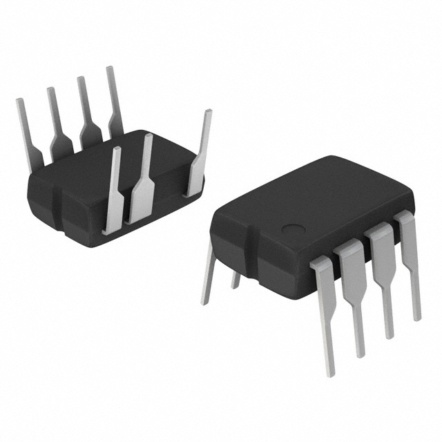
Package
DIP7AK:
Features
Switching Frequency=65 kHz, 100 kHz, 130 kHz
PWM Current Mode Control
Built-in Frequency Hopping Function
Burst Operation at Light Load
Frequency Reduction Function
Built-in 650 V Starter Circuit
Built-in 650 V Super Junction MOSFET
VCC Pin Under Voltage Protection
VCC Pin Over Voltage Protection
Over Current Limiter Function per Cycle
Over Current Limiter with AC Voltage Correction
Soft Start Function
Brown IN/OUT Function
ZT Pin OVP Function
1.00 mA(Typ)
0.30 mA(Typ)
65 kHz(Typ)
100 kHz(Typ)
130 kHz(Typ)
-40 °C to +105 °C
3.00 Ω(Typ)
W(Typ) x D(Typ) x H(Max)
9.27 mm x 6.35 mm x 8.63 mm
pitch 2.54 mm
Applications
Household Electrical Appliances, Adapters, etc.
Typical Application Circuit
FUSE
OUT
Filter
Diode
Bridge
DRAIN
SOURCE
BR
VCC
GND
〇Product structure : Silicon integrated circuit
.www.rohm.com
© 2018 ROHM Co., Ltd. All rights reserved.
TSZ22111 • 14 • 001
ZT
FB
GND
〇This product has no designed protection against radioactive rays
1/20
TSZ02201-0F1F0A200350-1-2
12.Sep.2018 Rev.001
�BM2P064E BM2P104E
BM2P134E
Pin Configuration
TOP VIEW
6
5
FB
7
GND
4
ZT
BR
3
VCC
SOURCE
2
DRAIN
1
Pin Description
Pin No.
Pin Name
I/O
Function
1
2
3
4
5
6
7
SOURCE
BR
GND
FB
ZT
VCC
DRAIN
I/O
I
I/O
I
I
I
I/O
MOSFET SOURCE pin
AC voltage detect pin
GND pin
Feedback signal input pin
Auxiliary winding input pin
Power supply input pin
MOSFET DRAIN pin
ESD Diode
VCC
GND
✔
✔
✔
✔
✔
✔
✔
Block Diagram
Filter
Diode
Bridge
BR
VCC
2
BR Comp
+
-
VCC UVLO
+
-
100 µs
Filter
100
µs
Filter
+
VCC OVP
ZT
DRAIN
6
5
7
Starter
Internal
Regulator
Gate
Clamper
Internal Block
ZT
OVP
100 µs Filter
+
-
3 counts Timer
Thermal
Protection
7V
OLP
64 ms
/512 ms
Timer
+
-
Super
Junction
MOSFET
PWM
Control
S
R Q
Internal
Regulator
4.0V
Burst
Comparator
+
PWM
Comparator
+
DRIVER
NOUT
Dynamic Current
+ Limitter
-
Logic
&
Timer
Current
Limitter
+
-
Reference
Voltage
LeadingEdge
Blanking
Time
1
SOURCE
Reference
Voltage
FB
4
Soft Start
1/4
MAX
DUTY
OSC
Frequency
Hopping
3
GND
www.rohm.com
© 2018 ROHM Co., Ltd. All rights reserved.
TSZ22111 • 15 • 001
2/20
TSZ02201-0F1F0A200350-1-2
12.Sep.2018 Rev.001
�BM2P064E BM2P104E
BM2P134E
Description of Blocks
1.
Starter Circuit (DRAIN: 7 pin)
This IC enables low standby electric power and high-speed startup because it has a built-in start circuit (650 V withstand
voltage). The current consumption after startup is OFF current ISTART3 (Typ=10 µA).
VH
Startup Current [A]
DRAIN
ISTART2
Starter
VCC
Cvcc
ISTART1
+
VCCUVLO
ISTART3
Figure 1. Start Circuit Block Diagram
2.
The VCC pin voltage
[V]
VUVLO1
Vsc
Figure 2. Startup Current vs the VCC Pin Voltage
Start Sequence (Soft Start Operation, Light Load Operation, Auto Restart Operation by Over Load Protection)
Start sequence is shown in Figure 3 and see the sections below for detailed descriptions.
VH
(Input Voltage)
VBR1
BR
VUVLO1
Under
tFOLP1
VCC
tFOLP2
tFOLP1
VFOLP1
FB
Output
Voltage
Normal
Load
Over
Load
Light
Load
Output
Current
Burst mode
Switching
Soft
Start
A
BC
D
E
F
G
H
I
Figure 3. Start Sequences Timing Chart
A:
B:
C:
D:
E:
F:
G:
H:
I:
The input voltage VH is applied to the IC. As VH voltage is applied, the BR pin voltage becomes higher than V BR1
(Typ=0.7 V).
When the VCC pin voltage exceeds VUVLO1 (Typ=13.5 V), the IC starts to operate. When the IC judges the other
protection functions as normal condition, switching operation starts. Until the secondary output voltage becomes a
constant value from startup, the VCC pin voltage drops by the VCC pin consumption current. When the VCC pin
voltage becomes VCHG1 (Typ=8.7 V) or less, the VCC pin charge operation starts.
Switching operation starts with the soft start function, over current limit value is restricted to prevent any excessive
rise in voltage or current. Output voltage will be set to rated voltage within the tFOLP1 (Typ=64 ms).
Once the output voltage is stable, the VCC pin voltage is also stable.
When the FB pin voltage becomes VBST1 (Typ=0.40 V) or less at light load, the IC starts burst operation to reduce
the power consumption.
When the FB pin voltage becomes VFOLP1 (Typ=3.4 V) or more, overload protection function operates.
When the FB pin voltage stays VFOLP1 (Typ=3.4 V) or more for tFOLP1 (Typ=64 ms) or more, switching stops. When
the FB pin voltage becomes VFOLP2 (Typ=3.2 V) or less, the IC’s internal FB OLP timer is reset.
Stopping switching continues for tFOLP2 (Typ=512 ms), the IC starts switching.
Same as D.
www.rohm.com
© 2018 ROHM Co., Ltd. All rights reserved.
TSZ22111 • 15 • 001
3/20
TSZ02201-0F1F0A200350-1-2
12.Sep.2018 Rev.001
�BM2P064E BM2P104E
BM2P134E
Description of Blocks – continued
3.
VCC Pin Protection Function
This IC has the internal protection functions at the VCC pin.
1) Under voltage protection function: VCC UVLO (Under Voltage Lockout)
2) Over voltage protection function: VCC OVP (Over Voltage Protection)
3) VCC charge function
The VCC charge function charges the VCC pin from the high voltage line through the starter circuit at startup time and
so on.
(1) VCC UVLO / VCC OVP Function
VCC UVLO function and VCC OVP function are auto recovery type protection function with voltage hysteresis.
Switching is stopped by the VCC OVP function when the VCC pin voltage ≥ VOVP1 (Typ=27.0 V), and restarts when
the VCC pin voltage ≤ VOVP2 (Typ=23.0 V).
VH
(Input Voltage)
VOVP1
VOVP2
VUVLO1
VCHG2
VCC
VCHG1
VUVLO2
Time
ON
ON
OFF
VCC UVLO
ON
VCC OVP
OFF
OFF
ON
ON
ON
VCC Charge
Function
OFF
OFF
ON
ON
OFF
OFF
Switching
OFF
A
B C
D
E F
G
H
I
J
A
Time
Figure 4. VCC UVLO / VCC OVP / VCC Charge Function Timing Chart
A:
B:
C:
D:
E:
F:
G:
H:
I:
J:
The VCC pin voltage starts to rises.
When the VCC pin voltage is VUVLO1 (Typ=13.5 V) or more, the VCC UVLO function is released and DC/DC
operation starts.
When the VCC pin voltage is VCHG1 (Typ=8.7 V) or less, the VCC charge function operates and the VCC pin
voltage rises.
When the VCC pin voltage is VCHG2 (Typ=13.0 V) or more, the VCC charge function stops.
When the status that the VCC pin voltage is VOVP1 (Typ=27.0 V) or more continues for tCOMP1 (Typ=100 μs),
switching is stopped by the VCC OVP function.
When the VCC pin voltage becomes VOVP2 (Typ=23.0 V) or less, switching operation restarts.
The VCC pin voltage drops.
Same as C.
Same as D.
When the input voltage VH drops and the VCC pin voltage becomes VUVLO2 (Typ=8.2 V) or less, switching
operation is stopped by the VCC UVLO function.
(2) VCC Charge Function
The IC starts to operate when the VCC pin voltage becomes VUVLO1 (Typ=13.5 V) or more. After that, the VCC charge
function operates when the VCC pin voltage becomes VCHG1 (Typ=8.7 V) or less. During this time, the VCC pin is
charged from the DRAIN pin through the starter circuit. By this operation, failure at startup is prevented. Once the
VCC charge function starts, it continues charge operation until the VCC pin voltage becomes VCHG2 (Typ=13.0 V) or
more, after which the charge function stops.
www.rohm.com
© 2018 ROHM Co., Ltd. All rights reserved.
TSZ22111 • 15 • 001
4/20
TSZ02201-0F1F0A200350-1-2
12.Sep.2018 Rev.001
�BM2P064E BM2P104E
BM2P134E
Description of Blocks – continued
4.
DC/DC Driver (PWM Comparator, Frequency Hopping, Slope Compensate, OSC, Burst)
This IC operates by current mode PWM control. The internal oscillator sets the switching frequency at a fixed value
when the FB pin voltage ≥ VDLT1 (Typ=1.25 V). It also has a built-in switching frequency hopping function.
Maximum duty cycle is fixed at 75 % (Typ) and minimum pulse width is fixed at 500 ns (Typ).
With current mode control, when the duty cycle exceeds 50 %, a sub harmonic oscillation may occur. As a
countermeasure, the IC has built-in slope compensation function.
This IC also has a built-in burst mode operation and frequency reduction operation to achieve lower power consumption
in light load.
The FB pin is pulled up by RFB (Typ=30 kΩ) to an internal regulator. The FB pin voltage varies with secondary output
voltage (secondary power). Burst mode operation and frequency reduction operation is determined by monitoring the
FB pin voltage.
(1) Frequency Reduction Circuit
Figure 5A to Figure 5C shows the FB pin voltage, switching frequency, and DC/DC operation modes.
mode 1: Burst voltage has hysteresis. Switching stops when the FB pin voltage ≤ VBST1 (Typ=0.4 V), and restarts
when the FB pin voltage ≥ VBST2 (Typ=0.45 V).
mode 2: When the FB pin voltage ≤ VDLT2 (Typ=0.65 V), switching frequency is at fSW2 (Typ=25 kHz, 27 kHz or 35 kHz).
At VDLT2 < the FB pin voltage ≤ VDLT1, switching frequency changes within the range of fSW1 to fSW2.
mode 3: Operates in fixed frequency fSW1 (Typ=65 kHz, 100 kHz or 130 kHz).
mode 4: If the IC detects over load status within a period of tFOLP1 (Typ=64 ms), it stops switching operation for tFOLP2
(Typ=512 ms).
Switching
Frequency
[kHz]
mode 1
mode 2
mode 3
Switching
Frequency
[kHz]
mode 4
mode 2
mode 3
mode 4
100
65
25
27
Pulse OFF
0.40
Pulse OFF
0.65
1.25
3.40 The FB pin
voltage[V]
Figure 5A. Switching Frequency vs the FB Pin Voltage
(BM2P064E)
Switching
Frequency
[kHz]
mode 1
mode 1
mode 2
mode 3
0.40
0.65
1.25
3.40 The FB pin
voltage[V]
Figure 5B. Switching Frequency vs the FB Pin Voltage
(BM2P104E)
mode 4
130
35
Pulse OFF
0.40
0.65
1.25
3.40
The FB pin
voltage[V]
Figure 5C. Switching Frequency vs the FB Pin Voltage
(BM2P134E)
(2) Frequency Hopping Function
Frequency hopping function achieves low EMI by changing the frequency at random. The pulse width changes in the
range of ±6 % for base frequency.
www.rohm.com
© 2018 ROHM Co., Ltd. All rights reserved.
TSZ22111 • 15 • 001
5/20
TSZ02201-0F1F0A200350-1-2
12.Sep.2018 Rev.001
�BM2P064E BM2P104E
4.
BM2P134E
DC/DC Driver – continued
(3) Over Current Limiter
This IC has a built-in over current limiter per cycle. When the SOURCE pin voltage becomes VCSA (Typ=0.4 V) or VCSB
(Typ=0.3 V) or more for 1 pulse, switching is turned off after passing internal delay time. The delay time varies in
relation to the time by which the SOURCE pin voltage reaches VCSA (Typ=0.4 V) or VCSB (Typ=0.3 V). By this time, AC
voltage correction function operates. The relations of the time until the SOURCE pin voltage reaches VCSA (Typ=0.4
V) or VCSB (Typ=0.3 V) and the additional delay time are shown in below.
Figure 6A. Delay Time vs the Time by Which the
SOURCE Pin Voltage Reaches VCSA (Typ=0.4 V)
(BM2P064E)
Figure 6B. Delay Time vs the Time by Which the
SOURCE Pin Voltage Reaches VCSB (Typ=0.3 V)
(BM2P104E)
Figure 6C. Delay Time vs the Time by Which the
SOURCE Pin Voltage Reaches VCSB (Typ=0.3 V)
(BM2P134E)
Ip is calculated by the following formula.
𝐼𝑝 =
𝑉𝑖𝑛
𝐿𝑝
× (𝑡𝑂𝑁 + 𝑡𝐷 + 𝑡𝐷𝐸𝐿𝐴𝑌 )
[A]
where:
𝑉𝑖𝑛 is the AC Input Voltage.
𝐿𝑝 is the Primary Inductance.
𝑡𝑂𝑁 is the Time to VCSA or VCSB.
𝑡𝐷 is the Additional Delay Time introduced by the IC (Refer to Figure 6A to Figure 6C).
𝑡𝐷𝐸𝐿𝐴𝑌 is the Delay Time peculiar to the IC (Typ=0.2 μs).
It is necessary to evaluate application in the end and adjust sense resistor and so on.
www.rohm.com
© 2018 ROHM Co., Ltd. All rights reserved.
TSZ22111 • 15 • 001
6/20
TSZ02201-0F1F0A200350-1-2
12.Sep.2018 Rev.001
�BM2P064E BM2P104E
4.
BM2P134E
DC/DC Driver – continued
(4) Dynamic Over Current Limiter
This IC has a built-in dynamic over current limiter circuit. When the SOURCE pin voltage becomes VDCS (Typ=1.05 V)
or more for two consecutive times, it stops switching operation for tDCS (Typ=128 μs).
VDCS
Dynamic
Current Limitter
2 Count
2
1
SOURCE
Voltage
tDCS
DC/DC ON
DC/DC
DC/DC OFF
Figure 7. State Transition of Switching Frequency
(5) Soft Start Function
This function controls the over current limiter value in order to prevent any excessive rise in voltage or current upon
startup. Figure 8 shows the details of soft start function. The IC implements soft start function by changing the over
current limiter value with time.
SOURCE Voltage[V]
VCS
VDCS
V D CS
V D CS x 0.75
V D CS x 0.50
VC S
V D CS x 0.25
V C S x 0.75
V C S x 0.50
V C S x 0.25
8.0
2.0 4.0
Time [ms]
Figure 8. The SOURCE Pin Voltage vs Time
(6) L.E.B. Time
When MOSFET is turned ON, surge current occurs by capacitive elements and drive current. During this time, there is
a probability of detection error in the over current limiter circuit due to a rise in the SOURCE pin voltage. To prevent it,
there is a built-in L.E.B. function (Leading Edge Blanking function) to mask the SOURCE pin voltage for tLEB (Typ=250
ns) after turn ON.
www.rohm.com
© 2018 ROHM Co., Ltd. All rights reserved.
TSZ22111 • 15 • 001
7/20
TSZ02201-0F1F0A200350-1-2
12.Sep.2018 Rev.001
�BM2P064E BM2P104E
BM2P134E
Description of Blocks – continued
5.
SOURCE Pin Short Protection
When the SOURCE pin is shorted to ground, the IC may overheat and get destroyed. To prevent destruction, it has a
built-in short protection function. Switching is turned off in tCSSHT (Typ=2.0 µs) ON width when the status that the
SOURCE pin voltage is VCSSHT (Typ=0.06 V) or less is detected by this function.
6.
Output Over Load Protection Function (FB OLP Comparator)
Output over load protection function monitors the load condition and stops switching operation when over load condition
is detected. The IC detects over load status at the FB pin voltage ≥ VFOLP1 (Typ=3.4 V) and releases FB OLP at the FB
pin voltage ≤ VFOLP2 (Typ=3.2 V). As output voltage decreases during over load condition and this condition continues for
tFOLP1 (Typ=64 ms), over load condition is detected and switching operation stops. FB OLP detection will be released
after the auto-recovery period tFOLP2 (Typ=512 ms).
7.
Input Voltage Protection Function (Brown IN/OUT)
This IC has a built-in UVLO function that monitors the input voltage through the BR pin. It prevents the IC from heating
by over-current when the input voltage is low. When BR UVLO function is released, IC operates by soft start. The BR pin
capacitor must be connected to prevent malfunction.
e.g. The case that BR UVLO is released when the input voltage is 130 Vac.
130𝑉×√2×𝑅𝐵𝑅2
𝑅𝐵𝑅1 +𝑅𝐵𝑅2
= 𝑉𝐵𝑅1
[V]
When RBR1 is set to 1.23 MΩ, RBR2 is calculated to 4.7 kΩ. Then, BR UVLO voltage is calculated as:
(𝑅𝐵𝑅1 +𝑅𝐵𝑅2 )×𝑉𝐵𝑅2
𝑅𝐵𝑅2 ×√2
= 71
[Vac]
Therefore, the hysteresis is 59 Vac.
FUSE
OUT
Filter
Diode
Bridge
VCC
6
3
GND
7
2
BR
RBR2
DRAIN
1
SOURCE
RBR1
5
ZT
4
FB
GND
Figure 9. Brown IN/OUT Circuit Example.
www.rohm.com
© 2018 ROHM Co., Ltd. All rights reserved.
TSZ22111 • 15 • 001
8/20
TSZ02201-0F1F0A200350-1-2
12.Sep.2018 Rev.001
�BM2P064E BM2P104E
BM2P134E
Description of Blocks – continued
8.
ZT Pin Over Voltage Protection
ZT OVP has 2 protection functions (Pulse detection and DC detection), both operate by latch protection.
(1)
Pulse Detection
After the ZT pin voltage becomes VZTOVP (Typ=3.5 V) or more for 3 consecutive switching times and continues for
tZTOVP (Typ=100 µs), the IC detects ZT OVP.
ON
OFF
Inner Gate
1 count
2 count
3 count
VZTOVP
ZT
tZTOVP
LATCH
Function
A
B
C
E
D
Figure 10. The ZT Pin Over Voltage Protection (Pulse Detection)
A:
B:
C:
D:
E:
(2)
Normal operation because the ZT pin voltage < VZTOVP (Typ=3.5 V)
The ZT pin voltage ≥ VZTOVP (Typ=3.5 V) is detected.
The second of the ZT pin voltage ≥ VZTOVP (Typ=3.5 V) is detected.
The third of the ZT pin voltage ≥ VZTOVP (Typ=3.5 V) is detected. Then internal timer starts to operate because of
detection of the three times continuation.
After tZTOVP (Typ=100 µs) from the three times detection, the IC stops by latch.
DC Detection
When ZT voltage ≥ VZTOVP (Typ=3.5 V) status continues for tZTOVP (Typ=100 µs), IC detects ZT OVP.
Less than
tZTOVP
tZTOVP
PULSE
VZTOVP
PULSE
ZT
ON
Switching
A
B
C
D
Figure 11. The ZT Pin Over Voltage Protection (DC Detection)
The ZT pin voltage ≥ VZTOVP (Typ=3.5 V)
Because the ZT pin voltage ≥ VZTOVP (Typ=3.5 V) status is less than tZTOVP (Typ=100 µs) period, DC/DC returns
to normal operations.
C: The ZT pin voltage ≥ VZTOVP (Typ=3.5 V)
D: Because the ZT pin voltage ≥ VZTOVP (Typ=3.5 V) status continues for tZTOVP (Typ=100 µs), latching occurs and
DC/DC is turned OFF.
A:
B:
www.rohm.com
© 2018 ROHM Co., Ltd. All rights reserved.
TSZ22111 • 15 • 001
9/20
TSZ02201-0F1F0A200350-1-2
12.Sep.2018 Rev.001
�BM2P064E BM2P104E
BM2P134E
Description of Blocks – continued
9.
ZT Trigger Mask Function
When switching is set ON / OFF, the superposition of noise may occur at the ZT pin. During this time, the detection
function is turned OFF for the duration of tZTMASK (Typ=0.60 µs) to prevent the ZT pin part from false detection.
ON
OFF
DC/DC
DRAIN
ZT
ZT Mask
Function
tZTMASK
A
B C
tZTMASK
D
E
F
G
Figure 12. ZT Trigger Mask Function
A:
B:
C:
D:
E:
F:
G:
DC/DC OFF → ON
DC/DC ON → OFF
Because noise occurs at the ZT pin, the ZT pin protection function is not operated for tZTMASK (Typ=0.60 µs).
Same as A.
Same as B
Same as C
Same as A
www.rohm.com
© 2018 ROHM Co., Ltd. All rights reserved.
TSZ22111 • 15 • 001
10/20
TSZ02201-0F1F0A200350-1-2
12.Sep.2018 Rev.001
�BM2P064E BM2P104E
BM2P134E
Absolute Maximum Ratings (Ta=25 °C)
Parameter
Maximum Applied Voltage 1
Maximum Applied Voltage 2
Maximum Applied Voltage 3
DRAIN Current (DC)
DRAIN Current (Pulse)
Power Dissipation
Maximum Junction Temperature
Storage Temperature Range
Symbol
Rating
Unit
VMAX1
VMAX2
VMAX3
IDD1
IDD2
Pd
Tjmax
Tstg
-0.3 to +650.0
-0.3 to +35.0
-0.3 to +6.5
1.7
4.0
1.00
150
-55 to +150
V
V
V
A
A
W
°C
°C
Conditions
DRAIN
VCC
BR, FB, SOURCE, ZT
PW =10 μs, Duty cycle=1 %
Caution 1:
Operating the IC over the absolute maximum ratings may damage the IC. The damage can either be a short circuit between pins or an open circuit
between pins and the internal circuitry. Therefore, it is important to consider circuit protection measures, such as adding a fuse, in case the IC is
operated over the absolute maximum ratings.
Caution 2: Should by any chance the maximum junction temperature rating be exceeded the rise in temperature of the chip may result in deterioration of the
properties of the chip. In case of exceeding this absolute maximum rating, design a PCB with power dissipation taken into consideration by increasing
board size and copper area so as not to exceed the maximum junction temperature rating.
(Note 1) Reduce by 8.0 mW/°C when operating Ta=25 °C or more when mounted on 70 mm x 70 mm x 1.6 mm thick, glass epoxy on single-layer substrate.
Thermal Loss
The thermal design should set operation for the following conditions.
1. The ambient temperature Ta must be 105 °C or less.
2. The IC’s loss must be within the power dissipation Pd.
The thermal reduction characteristics are as follows.
(PCB: 70 mm x 70 mm x 1.6 mm mounted on glass epoxy single layer substrate)
Figure 13. Thermal Reduction Characteristics
www.rohm.com
© 2018 ROHM Co., Ltd. All rights reserved.
TSZ22111 • 15 • 001
11/20
TSZ02201-0F1F0A200350-1-2
12.Sep.2018 Rev.001
�BM2P064E BM2P104E
BM2P134E
Recommended Operating Condition
Parameter
Power Supply Voltage Range 1
Power Supply Voltage Range 2
Operating Temperature
Symbol
VDRAIN
VCC
Topr
Specification
Min
Typ
Max
8.90
-40
15.00
+25
650
26.00
+105
Unit
V
V
°C
Conditions
DRAIN
VCC(Note 2)
Surrounding Temperature
(Note 2) The VCC recharge function operates in the VCC pin voltage range of less than 8.7 V (Refer to P-4 [3-2] the VCC charge function)
Recommended External Component Condition
Parameter
BR Pin Capacitor
Symbol
CBR
Recommended
0.01 or more
Unit
μF
Conditions
Electrical Characteristics in MOSFET Part (Unless otherwise noted, Ta=25 °C, VCC=15 V)
Parameter
DRAIN to SOURCE Voltage
DRAIN Leak Current
ON Resistance
Specifications
Symbol
VDDS
IDSS
RDS(ON)
Min
650
-
Typ
0
3.00
Max
100
3.40
Unit
Conditions
V
μA
Ω
ID=1 mA, VGS=0 V
VDS=650 V, VGS=0 V
ID=0.5 A, VGS=10 V
Electrical Characteristics in Starter Circuit Part (Unless otherwise noted, Ta=25 °C, VCC=15 V)
Parameter
Start Current 1
Start Current 2
OFF Current
Start Current Switching Voltage
www.rohm.com
© 2018 ROHM Co., Ltd. All rights reserved.
TSZ22111 • 15 • 001
Specifications
Symbol
ISTART1
ISTART2
ISTART3
VSC
Min
0.100
3.00
0.400
Typ
0.300
5.50
10
0.800
12/20
Unit
Max
0.600
8.50
20
1.200
mA
mA
μA
V
Conditions
VCC=0 V
VCC=10 V
TSZ02201-0F1F0A200350-1-2
12.Sep.2018 Rev.001
�BM2P064E BM2P104E
BM2P134E
Electrical Characteristics in Control IC Part (Unless otherwise noted, Ta=25 °C, VCC=15 V)
Parameter
Specifications
Symbol
Min
Typ
Max
Unit
Conditions
[Circuit Current]
Circuit Current (ON) 1
ION1
-
1000
1800
μA
Pulse Operation, VFB=2.0 V,
DRAIN =OPEN
Circuit Current (ON) 2
ION2
150
300
450
μA
Burst Operation, VFB=0.3 V
VUVLO1
VUVLO2
VUVLO3
VOVP1
VOVP2
VOVP3
tCOMP1
VLATCH
VCHG1
VCHG2
TSD1
TSD2
12.50
7.50
25.5
50
7.70
12.00
115
-
13.50
8.20
5.30
27.0
23.0
4.0
100
VUVLO2-0.5
8.70
13.00
145
75
14.50
8.90
28.5
150
9.70
14.00
175
-
V
V
V
V
V
V
μs
V
V
V
C
C
VCC rising
VCC falling
VUVLO3=VUVLO1-VUVLO2
VCC rising
VCC falling
TSD3
-
70
-
C
tCOMP2
50
100
150
μs
fSW1A
fSW2A
fDEL1A
fSW1B
fSW2B
fDEL1B
fSW1C
fSW2C
fDEL1C
tMIN
tSS1
tSS2
tSS3
DMAX
RFB
Gain
VBST1
VBST2
61.5
20
95.0
20
122.0
20
1.20
2.40
4.80
68.0
23
0.300
0.350
65.0
25
4.0
100.0
27
6.0
130.0
35
8.0
500
2.00
4.00
8.00
75.0
30
4.00
0.400
0.450
68.5
30
105.0
34
138.0
50
2.80
5.60
11.20
82.0
37
0.500
0.550
kHz
kHz
kHz
kHz
kHz
kHz
kHz
kHz
kHz
ns
ms
ms
ms
%
kΩ
V/V
V
V
VDLT1
1.10
1.25
1.40
V
VDLT2
0.50
0.65
0.80
V
VFOLP1
VFOLP2
tFOLP1
tFOLP2
VCSA
VCSB
3.20
3.00
40
358
0.380
0.280
3.40
3.20
64
512
0.400
0.300
3.60
3.40
88
666
0.420
0.320
V
V
ms
ms
V
V
VDCS
0.950
1.050
1.150
V
tDCS
64
128
196
μs
tLEB
-
250
-
ns
VCSSHT
0.030
0.060
0.090
V
tCSSHT
1.0
2.0
3.0
μs
[VCC Pin Protection Function]
VCC UVLO Voltage 1
VCC UVLO Voltage 2
VCC UVLO Hysteresis
VCC OVP Voltage 1
VCC OVP Voltage 2
VCC OVP Hysteresis
VCC OVP Timer
Latch Release VCC Voltage
VCC Charge Start Voltage
VCC Charge Stop Voltage
Over Temperature Protection 1(Note 3)
Over Temperature Protection 2(Note 3)
Over Temperature Protection
Hysteresis
Over Temperature Protection Timer
[PWM Type DC/DC Driver Block]
Switching Frequency 1A
Switching Frequency 2A
Frequency Hopping Width 1A
Switching Frequency 1B
Switching Frequency 2B
Frequency Hopping Width 1B
Switching Frequency 1C
Switching Frequency 2C
Frequency Hopping Width 1C
Minimum Pulse Width(Note 4)
Soft Start Time 1
Soft Start Time 2
Soft Start Time 3
Maximum Duty
FB Pin Pull-up Resistor
FB / CS Gain
FB Burst Voltage 1
FB Burst Voltage 2
Frequency Reduction Start
FB Voltage
Frequency Reduction Stop
FB Voltage
FB OLP Voltage 1
FB OLP Voltage 2
FB OLP ON Timer
FB OLP OFF Timer
Over Current Detection Voltage A
Over Current Detection Voltage B
Dynamic Over Current Detection
Voltage
Dynamic Over Current Detection
Timer
Leading Edge Blanking Time
SOURCE Pin Short Protection
Voltage
SOURCE Pin Short Protection Time
Control IC block’s Tj rising
Control IC block’s Tj falling
VFB=2.0 V (BM2P064E)
VFB=0.5 V (BM2P064E)
VFB=2.0 V (BM2P064E)
VFB=2.0 V (BM2P104E)
VFB=0.5 V (BM2P104E)
VFB=2.0 V (BM2P104E)
VFB=2.0 V (BM2P134E)
VFB=0.5 V (BM2P134E)
VFB=2.0 V (BM2P134E)
VFB falling
VFB rising
OLP detect VFB rising
OLP release VFB falling
BM2P064E
BM2P104E, BM2P134E
(Note 4)
(Note 3) Over temperature protection operates over Maximum Junction Temperature. Since, IC cannot guarantee for the operation over Maximum Junction
Temperature, always operate at Maximum Junction Temperature or less.
(Note 4) Not 100 % tested.
www.rohm.com
© 2018 ROHM Co., Ltd. All rights reserved.
TSZ22111 • 15 • 001
13/20
TSZ02201-0F1F0A200350-1-2
12.Sep.2018 Rev.001
�BM2P064E BM2P104E
BM2P134E
Electrical Characteristics in Control IC Part (Unless otherwise noted, Ta=25 °C, VCC=15 V) – continued
Parameter
Specifications
Symbol
[ BR Pin Function ]
BR Pin UVLO Detection Voltage 1
BR Pin UVLO Detection Voltage 2
BR Pin UVLO Hysteresis Voltage
BR Pin UVLO Detection Delay Time 1
BR Pin UVLO Detection Delay Time 2
[ ZT Pin Function ]
ZT OVP Voltage
ZT OVP Timer
ZT Trigger Mask Time
Unit
Min
Typ
Max
VBR1
VBR2
VBR3
tBR1
tBR2
0.64
0.32
50
64
0.70
0.38
0.32
100
128
0.76
0.44
150
196
V
V
V
μs
ms
VZTOVP
tZTOVP
tZTMASK
3.250
50
-
3.500
100
0.60
3.750
150
-
V
μs
µs
Conditions
VBR rising
VBR falling
VBR3=VBR1-VBR2
VBR rising
VBR falling
(Note 4)
(Note 4) Not 100 % tested.
Protection Circuit Operation Modes
The operation modes of the various protection functions of the IC are shown in Table 1.
Table 1. Protection Circuit Operation Modes
Function
VCC Pin
Under
Voltage
Protection
VCC Pin
Over Voltage
Protection
Thermal
Shutdown
FB Pin
Output
Over Load
Protection
SOURCE
Short
Protection
BR Pin
Under
Voltage
Protection
ZT Pin
Over Voltage
Protection
Detection
VCCVOVP1
(VCC
rising)
Tj>TSD1
(Tj rising)
VFB>VFOLP1
(VFB rising)
SOURCE<
VCSSHT
(tCSSHT=2.0
µs)
VBRVZTOVP
(pulse)
Release
VCC>VUVLO1
(VCC
rising)
VCC Pin B, the P-N junction operates as a parasitic transistor.
Parasitic diodes inevitably occur in the structure of the IC. The operation of parasitic diodes can result in mutual
interference among circuits, operational faults, or physical damage. Therefore, conditions that cause these diodes to
operate, such as applying a voltage lower than the GND voltage to an input pin (and thus to the P substrate) should be
avoided.
Resistor
Transistor (NPN)
Pin A
Pin B
C
E
Pin A
N
P+
P
N
N
P+
N
Pin B
B
Parasitic
Elements
N
P+
N P
N
P+
B
N
C
E
Parasitic
Elements
P Substrate
P Substrate
GND
GND
Parasitic
Elements
GND
Parasitic
Elements
GND
N Region
close-by
Figure 15. Example of Monolithic IC Structure
11. Ceramic Capacitor
When using a ceramic capacitor, determine a capacitance value considering the change of capacitance with
temperature and the decrease in nominal capacitance due to DC bias and others.
12. Thermal Shutdown Circuit(TSD)
This IC has a built-in thermal shutdown circuit that prevents heat damage to the IC. Normal operation should always
be within the IC’s maximum junction temperature rating. If however the rating is exceeded for a continued period, the
junction temperature (Tj) will rise which will activate the TSD circuit that will turn OFF power output pins. When the Tj
falls below the TSD threshold, the circuits are automatically restored to normal operation.
Note that the TSD circuit operates in a situation that exceeds the absolute maximum ratings and therefore, under no
circumstances, should the TSD circuit be used in a set design or for any purpose other than protecting the IC from
heat damage.
13. Over Current Protection Circuit (OCP)
This IC incorporates an integrated overcurrent protection circuit that is activated when the load is shorted. This
protection circuit is effective in preventing damage due to sudden and unexpected incidents. However, the IC should
not be used in applications characterized by continuous operation or transitioning of the protection circuit.
www.rohm.com
© 2018 ROHM Co., Ltd. All rights reserved.
TSZ22111 • 15 • 001
17/20
TSZ02201-0F1F0A200350-1-2
12.Sep.2018 Rev.001
�BM2P064E BM2P104E
BM2P134E
Ordering Information
B
M
2
P
x
x
4
E
06: 65 kHz
10: 100 kHz
13: 130 kHz
Lineup
Product
Number
BM2P064E
BM2P104E
BM2P134E
Switching
Frequency
(kHz)
65
100
130
MOSFET
RDS(ON) (Ω)
MOSFET
Withstand
Voltage(V)
Package
Orderable Part
Number
3.00
650
DIP7AK
BM2P064E
BM2P104E
BM2P134E
Making Diagram
DIP7AK (TOP VIEW)
Part Number Marking
LOT Number
Product Number
Part Number
Marking
BM2P064E
BM2P104E
BM2P134E
BM2P064E
BM2P104E
BM2P134E
www.rohm.com
© 2018 ROHM Co., Ltd. All rights reserved.
TSZ22111 • 15 • 001
18/20
TSZ02201-0F1F0A200350-1-2
12.Sep.2018 Rev.001
�BM2P064E BM2P104E
BM2P134E
Physical Dimension and Packing Information
Package Name
www.rohm.com
© 2018 ROHM Co., Ltd. All rights reserved.
TSZ22111 • 15 • 001
DIP7AK
19/20
TSZ02201-0F1F0A200350-1-2
12.Sep.2018 Rev.001
�BM2P064E BM2P104E
BM2P134E
Revision History
Date
Revision
12.Sep.2018
001
Changes
New Release
www.rohm.com
© 2018 ROHM Co., Ltd. All rights reserved.
TSZ22111 • 15 • 001
20/20
TSZ02201-0F1F0A200350-1-2
12.Sep.2018 Rev.001
�Notice
Precaution on using ROHM Products
1.
Our Products are designed and manufactured for application in ordinary electronic equipment (such as AV equipment,
OA equipment, telecommunication equipment, home electronic appliances, amusement equipment, etc.). If you
(Note 1)
intend to use our Products in devices requiring extremely high reliability (such as medical equipment
, transport
equipment, traffic equipment, aircraft/spacecraft, nuclear power controllers, fuel controllers, car equipment including car
accessories, safety devices, etc.) and whose malfunction or failure may cause loss of human life, bodily injury or
serious damage to property (“Specific Applications”), please consult with the ROHM sales representative in advance.
Unless otherwise agreed in writing by ROHM in advance, ROHM shall not be in any way responsible or liable for any
damages, expenses or losses incurred by you or third parties arising from the use of any ROHM’s Products for Specific
Applications.
(Note1) Medical Equipment Classification of the Specific Applications
JAPAN
USA
EU
CHINA
CLASSⅢ
CLASSⅡb
CLASSⅢ
CLASSⅢ
CLASSⅣ
CLASSⅢ
2.
ROHM designs and manufactures its Products subject to strict quality control system. However, semiconductor
products can fail or malfunction at a certain rate. Please be sure to implement, at your own responsibilities, adequate
safety measures including but not limited to fail-safe design against the physical injury, damage to any property, which
a failure or malfunction of our Products may cause. The following are examples of safety measures:
[a] Installation of protection circuits or other protective devices to improve system safety
[b] Installation of redundant circuits to reduce the impact of single or multiple circuit failure
3.
Our Products are designed and manufactured for use under standard conditions and not under any special or
extraordinary environments or conditions, as exemplified below. Accordingly, ROHM shall not be in any way
responsible or liable for any damages, expenses or losses arising from the use of any ROHM’s Products under any
special or extraordinary environments or conditions. If you intend to use our Products under any special or
extraordinary environments or conditions (as exemplified below), your independent verification and confirmation of
product performance, reliability, etc, prior to use, must be necessary:
[a] Use of our Products in any types of liquid, including water, oils, chemicals, and organic solvents
[b] Use of our Products outdoors or in places where the Products are exposed to direct sunlight or dust
[c] Use of our Products in places where the Products are exposed to sea wind or corrosive gases, including Cl2,
H2S, NH3, SO2, and NO2
[d] Use of our Products in places where the Products are exposed to static electricity or electromagnetic waves
[e] Use of our Products in proximity to heat-producing components, plastic cords, or other flammable items
[f] Sealing or coating our Products with resin or other coating materials
[g] Use of our Products without cleaning residue of flux (even if you use no-clean type fluxes, cleaning residue of
flux is recommended); or Washing our Products by using water or water-soluble cleaning agents for cleaning
residue after soldering
[h] Use of the Products in places subject to dew condensation
4.
The Products are not subject to radiation-proof design.
5.
Please verify and confirm characteristics of the final or mounted products in using the Products.
6.
In particular, if a transient load (a large amount of load applied in a short period of time, such as pulse. is applied,
confirmation of performance characteristics after on-board mounting is strongly recommended. Avoid applying power
exceeding normal rated power; exceeding the power rating under steady-state loading condition may negatively affect
product performance and reliability.
7.
De-rate Power Dissipation depending on ambient temperature. When used in sealed area, confirm that it is the use in
the range that does not exceed the maximum junction temperature.
8.
Confirm that operation temperature is within the specified range described in the product specification.
9.
ROHM shall not be in any way responsible or liable for failure induced under deviant condition from what is defined in
this document.
Precaution for Mounting / Circuit board design
1.
When a highly active halogenous (chlorine, bromine, etc.) flux is used, the residue of flux may negatively affect product
performance and reliability.
2.
In principle, the reflow soldering method must be used on a surface-mount products, the flow soldering method must
be used on a through hole mount products. If the flow soldering method is preferred on a surface-mount products,
please consult with the ROHM representative in advance.
For details, please refer to ROHM Mounting specification
Notice-PGA-E
© 2015 ROHM Co., Ltd. All rights reserved.
Rev.003
�Precautions Regarding Application Examples and External Circuits
1.
If change is made to the constant of an external circuit, please allow a sufficient margin considering variations of the
characteristics of the Products and external components, including transient characteristics, as well as static
characteristics.
2.
You agree that application notes, reference designs, and associated data and information contained in this document
are presented only as guidance for Products use. Therefore, in case you use such information, you are solely
responsible for it and you must exercise your own independent verification and judgment in the use of such information
contained in this document. ROHM shall not be in any way responsible or liable for any damages, expenses or losses
incurred by you or third parties arising from the use of such information.
Precaution for Electrostatic
This Product is electrostatic sensitive product, which may be damaged due to electrostatic discharge. Please take proper
caution in your manufacturing process and storage so that voltage exceeding the Products maximum rating will not be
applied to Products. Please take special care under dry condition (e.g. Grounding of human body / equipment / solder iron,
isolation from charged objects, setting of Ionizer, friction prevention and temperature / humidity control).
Precaution for Storage / Transportation
1.
Product performance and soldered connections may deteriorate if the Products are stored in the places where:
[a] the Products are exposed to sea winds or corrosive gases, including Cl2, H2S, NH3, SO2, and NO2
[b] the temperature or humidity exceeds those recommended by ROHM
[c] the Products are exposed to direct sunshine or condensation
[d] the Products are exposed to high Electrostatic
2.
Even under ROHM recommended storage condition, solderability of products out of recommended storage time period
may be degraded. It is strongly recommended to confirm solderability before using Products of which storage time is
exceeding the recommended storage time period.
3.
Store / transport cartons in the correct direction, which is indicated on a carton with a symbol. Otherwise bent leads
may occur due to excessive stress applied when dropping of a carton.
4.
Use Products within the specified time after opening a humidity barrier bag. Baking is required before using Products of
which storage time is exceeding the recommended storage time period.
Precaution for Product Label
A two-dimensional barcode printed on ROHM Products label is for ROHM’s internal use only.
Precaution for Disposition
When disposing Products please dispose them properly using an authorized industry waste company.
Precaution for Foreign Exchange and Foreign Trade act
Since concerned goods might be fallen under listed items of export control prescribed by Foreign exchange and Foreign
trade act, please consult with ROHM in case of export.
Precaution Regarding Intellectual Property Rights
1.
All information and data including but not limited to application example contained in this document is for reference
only. ROHM does not warrant that foregoing information or data will not infringe any intellectual property rights or any
other rights of any third party regarding such information or data.
2.
ROHM shall not have any obligations where the claims, actions or demands arising from the combination of the
Products with other articles such as components, circuits, systems or external equipment (including software).
3.
No license, expressly or implied, is granted hereby under any intellectual property rights or other rights of ROHM or any
third parties with respect to the Products or the information contained in this document. Provided, however, that ROHM
will not assert its intellectual property rights or other rights against you or your customers to the extent necessary to
manufacture or sell products containing the Products, subject to the terms and conditions herein.
Other Precaution
1.
This document may not be reprinted or reproduced, in whole or in part, without prior written consent of ROHM.
2.
The Products may not be disassembled, converted, modified, reproduced or otherwise changed without prior written
consent of ROHM.
3.
In no event shall you use in any way whatsoever the Products and the related technical information contained in the
Products or this document for any military purposes, including but not limited to, the development of mass-destruction
weapons.
4.
The proper names of companies or products described in this document are trademarks or registered trademarks of
ROHM, its affiliated companies or third parties.
Notice-PGA-E
© 2015 ROHM Co., Ltd. All rights reserved.
Rev.003
�Datasheet
General Precaution
1. Before you use our Products, you are requested to carefully read this document and fully understand its contents.
ROHM shall not be in any way responsible or liable for failure, malfunction or accident arising from the use of any
ROHM’s Products against warning, caution or note contained in this document.
2. All information contained in this document is current as of the issuing date and subject to change without any prior
notice. Before purchasing or using ROHM’s Products, please confirm the latest information with a ROHM sales
representative.
3.
The information contained in this document is provided on an “as is” basis and ROHM does not warrant that all
information contained in this document is accurate and/or error-free. ROHM shall not be in any way responsible or
liable for an y damages, expenses or losses incurred b y you or third parties resulting from inaccuracy or errors of or
concerning such information.
Notice – WE
© 2015 ROHM Co., Ltd. All rights reserved.
Rev.001
�