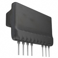
BP5319X

BP5319X

  • 厂商:

    ROHM(罗姆)

  • 封装:

    SIP9_7Pin

  • 描述:

    IC CONV DC/DC -24V 30MA SIP9LF

  • 详情介绍
  • 数据手册
  • 价格&库存
BP5319X 数据手册
DC / DC converter for LCDs BP5319 / BP5319X The BP5319 and BP5319X are DC / DC converters for supplying power to liquid crystal displays (LCDs) panels. These modules supply a negative voltage from power supply of 5V. They are available in a single in-line package as an upright (BP5319) or L-shaped lead (BP5319X) type. Applications LCD panels in copiers, facsimiles, personal computers, word processors, instruments, and other displays Features 1) Accurate output voltage. (−24V±0.75V) 2) High conversion efficiency. (typically 75%) 3) The external resistor can change an output voltage. 4) Built-in protection circuit. 5) Built-in ON/OFF switch. 6) Compact and light. 7) Available as an upright or L-shaped lead type. Absolute maximum ratings (Ta=25°C) Parameter Input voltage Output current ON / OFF CTL voltage Operating temperature range Storage temperature range Symbol VIN Io VCTL Topr Tstg Limits 7 30 7 −10~+60 −30~+85 Unit V mA V °C °C 1/5 BP5319 / BP5319X Pin descriptions Pin No. 1 2 3 4, 7 8 9 Pin name CO VOUT Vref GND VCTL VIN Function Output smoothing capacitor connection pin; connect a low-impedance capacitor with a recommended capacitance of 47 µ F between this pin and GND. Output pin Output voltage adjustment pin for contrast; output voltages is adjusted by connecting a resistor between pins 2 and 3 or pins 3 and 4. Ground pin; pins 4 and 7 are internal connection. Output ON / OFF control pin; output starts when the pin is LOW level or OPEN, and stops when the pin HIGH level. Input pin; connect a low-impedance capacitor with a recommended capacitance of 100mF between this pin and GND. Electrical characteristics Parameter (Unless otherwise noted, Ta=25°C) Symbol Min. Typ. Max. Unit V Conditions Input voltage Output current Output voltage Line regulation Load regulation Output voltage temperature coefficient Ripple noise voltage Conversion efficiency ON / OFF CTL voltage when OFF ON / OFF CTL voltage when ON VIN IOUT VOUT ∆V1 ∆V2 ∆Vt ν1 η VCTL VCTL 4.5 − −24.75 − − − − 70 2.0 − − − 50 50 − − −24.00 − − −10 − 75 − − 5.5 30 −23.25 0.24 0.24 − 150 − − 0.5 mA V V V VIN=5V, IOUT=25mA VIN=4.5~5.5V, IOUT=25mA VIN=5V, IOUT=0~25mA ∗2 ∗1 mV / °C VIN=5V, IOUT=25mA mVPP % V V µA mA kΩ kΩ VIN=5V, IOUT=25mA VIN=5V, IOUT=25mA VIN=5V VIN=5V (Alternatively, when Open) ON / OFF CTL input current Current consumption when OFF R1 resistance R2 resistance ∗1 Measured with a bandwidth of 20MHz. ∗2 Ta=−10~60°C ICTL IOFF R1 R2 100 − − − 150 0.5 VIN=4.5~5.5V, VCTL=5V ∗2 VIN=4.5~5.5V, VCTL=5V ∗2 VIN=4.5~5.5V, VCTL=5V ∗2 VIN=4.5~5.5V, VCTL=5V ∗2 ∞ ∞ 2/5 BP5319 / BP5319X Measurement circuit BP5319 / BP5319X 1 2 3 4 7 8 9 VIN VOUT ON / OFF SW C2 C3 + C1 VCTL + GND GND Fig.1 C1 : 100µF / 16V (Low-impedance capacitor) C2 : 47µF / 35V (Low-impedance capacitor) C3 : 0.022µF / 50V (Ceramic capacitor) Application example (1) When increasing the output voltage (to negative voltage side) (2) When reducing the output voltage (near to zero voltage) BP5319 / BP5319X BP5319 / BP5319X 1 2 R1 3 4 7 8 9 Be sure to use fuse for safety 1 2 3 R2 4 7 8 9 Be sure to use fuse for safety VOUT C2 GND ON / OFF + C1 VIN VOUT C2 ON / OFF + C1 VIN + GND GND + GND Note) Set up the change of the output voltage in the range of the territory(Fig.2) which can be used. Operation notes (1) Place I/O external capacitors as near as possible to the connection pins. In particular, make sure to minimize the impedance between the input-side capacitor (C1) and pin 9. (Reference value: A length less than 50mm is recommended for a copper foil of 1.0mm wide and 35µm thick.) (2) Avoid frequent switching using the ON / OFF CTL pin (5 times per second at the maximum). 3/5 BP5319 / BP5319X Electrical characteristic curves −30 OUTPUT VOLTAGE : VO (V) −25 −20 −15 −10 −5 Unusable range Ta=60°C VIN OUTPUT VOLTAGE : VO (V) OUTPUT VOLTAGE : VO (V) =5 V ∗1. R1>50kΩ R1 2pin − 3pin R2
BP5319X
物料型号: - BP5319:直立型单列直插式封装。 - BP5319X:L型引脚单列直插式封装。

器件简介: BP5319和BP5319X是为液晶显示屏(LCD)供电的DC/DC转换器。这些模块能够从5V电源中提供负电压。它们分别以直立型和L型引脚的形式提供。

引脚分配: - 1号引脚:Co,输出平滑电容器连接引脚;在此引脚和地之间连接推荐电容值为47uF的低阻抗电容器。 - 2号引脚:VoUT,输出引脚。 - 3号引脚:Vref,用于对比度调整的输出电压调整引脚;通过在2号引脚和3号引脚或3号引脚和4号引脚之间连接电阻来调整输出电压。 - 4号引脚:GND,地引脚;4号引脚和7号引脚内部连接。 - 8号引脚:VCTL,输出开/关控制引脚;当引脚为低电平或开路时输出开始,当引脚为高电平时输出停止。 - 9号引脚:VN,输入引脚;在此引脚和地之间连接推荐电容值为100mF的低阻抗电容器。

参数特性: - 输入电压(VIN):7V - 输出电流(Io):30mA - 开/关控制电压(Vcn):7V - 工作温度范围(Topr):-10~+60°C - 存储温度范围(Tstg):-30~+85°C

功能详解: 1. 输出电压准确(-24V±0.75V)。 2. 高转换效率(典型值75%)。 3. 外部电阻可以改变输出电压。 4. 内置保护电路。 5. 内置开/关开关。 6. 紧凑轻便。 7. 提供直立型或L型引脚类型。

应用信息: 适用于复印机、传真机、个人电脑、文字处理器、仪器等LCD面板。

封装信息: - BP5319:SIP9封装。 - BP5319X:SIP9(L型)封装。
BP5319X 价格&库存

很抱歉,暂时无法提供与“BP5319X”相匹配的价格&库存,您可以联系我们找货

免费人工找货