Datasheet
Serial EEPROM Series Standard EEPROM
I2C BUS EEPROM (2-Wire)
BR24G512-3A
General Description
BR24G512-3A is a serial EEPROM of I2C BUS Interface Method
Features
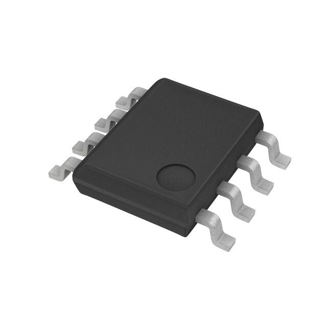
Packages W(Typ) x D(Typ)x H(Max)
All controls available by 2 ports of serial clock (SCL)
and serial data (SDA)
Other devices than EEPROM can be connected to the
same port, saving microcontroller port
1.7V to 5.5V single power source operation most
suitable for battery use
1.7V to 5.5V wide limit of operating voltage, possible
1MHz operation
Page Write Mode useful for initial value write at factory
shipment
Self-timed Programming Cycle
Low Current Consumption
Prevention of Write Mistake
Write (Write Protect) Function added
Prevention of Write Mistake at Low Voltage
More than 1 million write cycles
More than 40 years data retention
Noise filter built in SCL / SDA terminal
Initial delivery state FFh
Not Recommended for
New Designs
DIP-T8
SOP-J8
9.30mm x 6.50mm x 7.10mm
4.90mm x 6.00mm x 1.65mm
SOP8
TSSOP-B8
5.00mm x 6.20mm x 1.71mm
3.00mm x 6.40mm x 1.20mm
Figure 1.
Page Write
Number of
Pages
128 Bytes
Product number
BR24G512-3A
BR24G512-3A
Capacity
Bit
Format
Type
Power Supply
Voltage
DIP-T8*1
BR24G512-3A
BR24G512F-3A
512Kbit
64K×8
Package
SOP8
1.7V to 5.5V
BR24G512FJ-3A
BR24G512FVT-3A
SOP-J8
TSSOP-B8
*1 Not Recommended for New Designs.
〇Product structure: Silicon monolithic integrated circuit
.www.rohm.com
© 2014 ROHM Co., Ltd. All rights reserved.
TSZ22111 • 14 • 001
〇This product has no designed protection against radioactive rays
1/30
TSZ02201-0R2R0G100360-1-2
11.Jun.2019 Rev.005
�BR24G512-3A
Absolute Maximum Ratings (Ta=25°C)
Parameter
Symbol
Rating
Unit
Vcc
-0.3 to +6.5
V
Supply Voltage
Remark
0.45 (SOP8)
Power Dissipation
Derate by 4.5mW/°C when operating above Ta=25°C
0.45 (SOP-J8)
Pd
0.33 (TSSOP-B8)
0.80
Derate by 4.5mW/°C when operating above Ta=25°C
W
Derate by 3.3mW/°C when operating above Ta=25°C
(DIP-T8(1))
Derate by 8.0mW/°C when operating above Ta=25°C
Storage Temperature
Tstg
-65 to +150
°C
Operating Temperature
Topr
-40 to +85
°C
-
-0.3 to Vcc+1.0
V
The Max value of Input voltage/Output voltage is not over 6.5V.
When the pulse width is 50ns or less, the Min value of Input
voltage/Output voltage is not lower than -1.0V.
Tjmax
150
°C
Junction temperature at the storage condition
VESD
-4000 to +4000
V
Input Voltage /
Output Voltage
Junction
Temperature
Electrostatic discharge
voltage
(human body model)
(1) Not Recommended for New Designs.
Memory Cell Characteristics (Ta=25°C, VCC=1.7V to 5.5V)
Parameter
Min
1,000,000
40
Write Cycles (2)
Data Retention (2)
Limit
Typ
-
Max
-
Unit
Times
Years
(2) Not 100% TESTED
Recommended Operating Ratings
Parameter
Power Source Voltage
Input Voltage
Symbol
Vcc
VIN
Rating
1.7 to 5.5
0 to Vcc
Unit
V
DC Characteristics (Unless otherwise specified, Ta=-40°C to +85°C, Vcc =1.7V to 5.5V)
Parameter
Symbol
Limit
Min
Typ
Max
Unit
Conditions
Input High Voltage1
VIH1
0.7Vcc
-
Vcc+1.0
V
Input Low Voltage1
VIL1
-0.3(3)
-
+0.3Vcc
V
Output Low Voltage1
VOL1
-
-
0.4
V
Output Low Voltage2
VOL2
-
-
0.2
V
Input Leakage Current
ILI
-1
-
+1
μA
IOL=3.0mA,
2.5V≤Vcc≤5.5V (SDA)
IOL=0.7mA,
1.7V≤Vcc


 工商网监
湘ICP备2023018690号
工商网监
湘ICP备2023018690号

