Datasheet
Serial EEPROM Series Automotive EEPROM
105°C Operation SPI BUS EEPROM
BR25A512-3M
General Description
BR25A512-3M is a 512Kbit Serial EEPROM of SPI BUS Interface.
Features
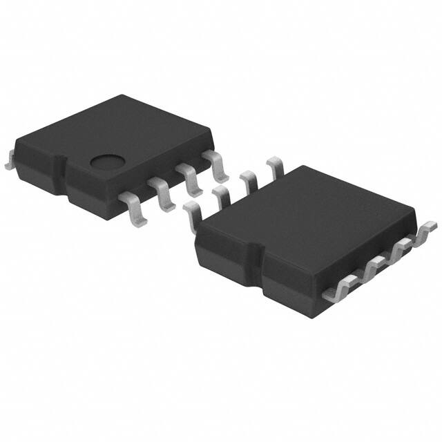
Packages W(Typ) x D(Typ) x H(Max)
High Speed Clock Action up to 10MHz (Max)
Wait Function by HOLDB Terminal
Part or Whole of Memory Arrays Settable as
Read only Memory Area by Program
2.5V to 5.5V Single Power Source Operation Most
Suitable for Battery Use
Up to 128 Bytes in Page Write Mode
For SPI Bus Interface (CPOL, CPHA) = (0, 0), (1, 1)
Self-timed Programming Cycle
Low Current Consumption
At Write Action (5V)
: 0.7mA (Typ)
At Read Action (5V)
: 2.4mA (Typ)
At Standby Action (5V)
: 0.1µA (Typ)
Address Auto Increment Function at Read Action
Prevention of Write Mistake
Write Prohibition at Power On
Write Prohibition by Command Code (WRDI)
Write Prohibition by WPB Pin
Write Prohibition Block Setting by Status Registers
(BP1, BP0)
Prevention of Write Mistake at Low Voltage
More than 100 years Data Retention
More than 1 Million Write Cycles
Bit Format 64K×8
Initial Delivery Data
Memory Array : FFh
Status Register : WPEN, BP1, BP0 : 0
○Product structure:Silicon monolithic integrated circuit
www.rohm.com
©2015 ROHM Co., Ltd. All rights reserved.
TSZ22111・14・001
SOP8
5.00mm x 6.20mm x 1.71mm
SOP- J8
4.90mm x 6.00mm x 1.65mm
TSSOP-B8
3.00mm x 6.40mm x 1.20mm
Figure 1.
○This product is not designed protection against radioactive rays
1/29
TSZ02201-0R2R0G100750-1-2
6.Oct.2015 Rev.001
�Datasheet
BR25A512-3M
Absolute Maximum Ratings (Ta=25°C)
Parameter
Supply Voltage
Power Dissipation
Storage Temperature
Operating Temperature
Input Voltage /
Output Voltage
Junction Temperature
Electrostatic discharge
voltage
(human body model)
Symbol
VCC
Unit
V
Tstg
Topr
Ratings
-0.3 to +6.5
0.45 (SOP8)
0.45 (SOP-J8)
0.33 (TSSOP-B8)
- 65 to +150
- 40 to +105
‐
- 0.3 to Vcc+1.0
V
Tjmax
150
°C
VESD
-4000 to +4000
V
Pd
Remarks
When using at Ta=25°C or higher 4.5mW to be reduced per 1°C.
W
When using at Ta=25°C or higher 4.5mW to be reduced per 1°C.
When using at Ta=25°C or higher 3.3mW to be reduced per 1°C.
°C
°C
The Max value of Input Voltage/Output Voltage is not over 6.5V.
When the pulse width is 50ns or less, the Min value of Input
Voltage/Output Voltage is not under -1.0V.
Junction temperature at the storage condition
Caution: Operating the IC over the absolute maximum ratings may damage the IC. The damage can either be a short circuit between pins or an open circuit
between pins and the internal circuitry. Therefore, it is important to consider circuit protection measures, such as adding a fuse, in case the IC is operated over
the absolute maximum ratings.
Memory Cell Characteristics (Ta=25°C, Vcc=2.5V to 5.5V)
Parameter
Limits
Typ
-
Min
1,000,000
150,000
100
20
Write Cycles (Note1)
Data Retention (Note1)
Max
-
Unit
Condition
Times
Times
Years
Years
Ta≤25°C
Ta≤105°C
Ta≤25°C
Ta≤105°C
(Note1) Not 100% TESTED
Recommended Operating Ratings
Parameter
Power Source Voltage
Input Voltage
Bypass capacitor
Ratings
Symbol
Min
2.5
0
0.1
Vcc
VIN
C
Max
5.5
VCC
-
Unit
V
V
µF
Input / Output Capacity (Ta=25°C, frequency=5MHz)
Parameter
Input Capacity (Note1)
Output Capacity (Note1)
Symbol
CIN
COUT
Min
-
Max
8
8
Unit
pF
Conditions
VIN=GND
VOUT=GND
(Note1) Not 100% TESTED.
DC Characteristics (Unless otherwise specified, Ta=-40°C to +105°C, Vcc=2.5V to 5.5V)
VIH
VIL
VOL
VOH
ILI
ILO
Min
0.7 x Vcc
-0.3 (Note1)
0
Vcc-0.2
-1
-1
Limits
Typ
-
Max
Vcc+1.0
0.3 x Vcc
0.4
Vcc
1
1
ICC1
-
-
1.5
mA
ICC2
-
-
2
mA
Supply Current (Read)
ICC3
-
-
4
mA
Standby Current
ISB
-
-
10
µA
Parameter
Input High Voltage
Input Low Voltage
Output Low Voltage
Output High Voltage
Input Leakage Current
Output Leakage Current
Symbol
Unit
V
V
V
V
µA
µA
Supply Current (Write)
Conditions
IOL=3.0mA
IOH=-2.0mA
VIN=0 to Vcc
VOUT=0 to Vcc, CSB=Vcc
Vcc=2.5V, fSCK=5MHz, tE/W=5ms
Byte Write, Page Write, Write Status Register
Vcc=5.5V, fSCK=10MHz, tE/W=5ms
Byte Write, Page Write, Write Status Register
Vcc=5.5V, fSCK=10MHz, SO=OPEN
Read, Read Status Register
VIH/VIL=0.9Vcc/0.1Vcc
Vcc=5.5V, SO=OPEN
CSB=HOLDB=WPB=Vcc, SCK=SI=Vcc or GND
(Note1) When the pulse width is 50ns or less, it is -1.0V.
www.rohm.com
©2015 ROHM Co., Ltd. All rights reserved.
TSZ22111・15・001
2/29
TSZ02201-0R2R0G100750-1-2
6.Oct.2015 Rev.001
�Datasheet
BR25A512-3M
AC Characteristics (Ta=-40°C to +105°C, 2.5V≤Vcc
很抱歉,暂时无法提供与“BR25A512F-3MGE2”相匹配的价格&库存,您可以联系我们找货
免费人工找货- 国内价格 香港价格
- 2500+12.045402500+1.55938
- 国内价格 香港价格
- 1+15.282761+1.97849
- 10+14.3254510+1.85456
- 25+13.9167025+1.80164
- 50+13.6072050+1.76157
- 100+13.29685100+1.72140
- 250+12.88486250+1.66806
- 500+12.57449500+1.62788
- 1000+12.266291000+1.58798
- 国内价格 香港价格
- 1+14.901131+1.92908
- 10+14.3040910+1.85179
- 30+10.8545230+1.40522
- 50+10.1662750+1.31611
- 100+9.65215100+1.24956
- 300+9.30388300+1.20447
- 500+9.23754500+1.19588
- 国内价格
- 1+7.26000
- 100+6.05000
- 1250+5.51100
- 2500+5.28000