Datasheet
CMOS LDO Regulator Series for Automotive
Ultra-Small Package
FULL CMOS LDO Regulator
BUxxJA2MNVX-C series
General Description
Key Specifications
BUxxJA2MNVX-C series are high-performance FULL
CMOS regulators with 200mA output, which are mounted
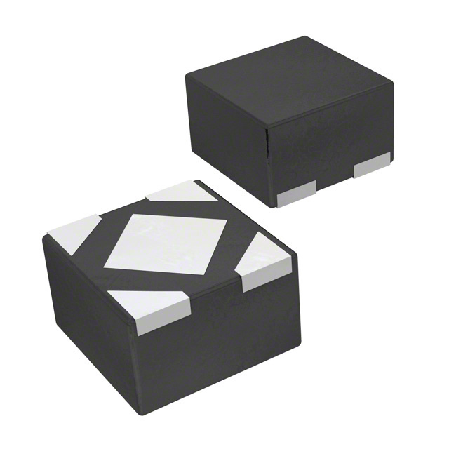
on versatile package SSON004R1010 (1.00mm x 1.00
mm x 0.60mm). These devices have excellent noise
characteristics and load responsiveness characteristics
despite its low circuit current consumption of 35μA. They
are most appropriate for various applications such as
power supplies for radar and camera of the automotive.
Input Voltage Range:
1.7V to 6.0V
Output Voltage:
1.0V to 3.4V
Output Voltage Accuracy: ±2.0%(Ta=-40°C to 125°C)
Output Current:
200mA(Max)
Standby Current:
35μA (Typ)
Operating Temperature Range:
-40°C to +125°C
Package
Features
SSON004R1010 :
W(Typ) x D(Typ) x H(Max)
1.00mm x 1.00mm x 0.60mm
AEC-Q100 Qualified(Note 1)
High Accuracy Output
Low Current Consumption
Compatible With Small Ceramic Capacitor(CIN=CO=0.47μF)
With Built-in Output Discharge Circuit
High Ripple Rejection
ON/OFF Control of Output Voltage
Built-in Over Current Protection Circuit
Built-in Thermal Shutdown Circuit
(Note 1) Grade1
SSON004R1010
Applications
Radar and camera for automotive, etc.
Typical Application Circuit
STBY
VIN
CIN
0.47μF
STBY
VOUT
VIN
VOUT
CO
0.47μF
GND
GND
GND
Figure 1. Application Circuit
〇Product structure : Silicon monolithic integrated circuit
.www.rohm.com
© 2014 ROHM Co., Ltd. All rights reserved.
TSZ22111 • 14 • 001
〇This product has no designed protection against radioactive rays
1/23
TSZ02201-0G5G1AD00060-1-2
9.Jul.2018 Rev.006
�BUxxJA2MNVX-C series
Ordering Information
B
U
Part Number
x
x
J
A
2
M
Output Voltage Output Current Category
10 : 1.0V
200mA
M:Automotive
11 : 1.1V
12 : 1.2V
1C : 1.25V
15 : 1.5V
18 : 1.8V
25 : 2.5V
28 : 2.8V
2J : 2.85V
29 : 2.9V
30 : 3.0V
33 : 3.3V
34 : 3.4V
N
V
X
-
Package
C TL
Product Rank
C:for Automotive
Packaging and forming
specification
TL: Embossed tape and reel
NVX:SSON004R1010
Block Diagram
Figure 2. Block Diagram
Pin Descriptions
Pin Configurations
4 VIN
Pin No.
Pin name
1
VOUT
Output Voltage
2
GND
Ground
3
STBY
ON/OFF control of output voltage (High: ON, Low: OFF)
4
VIN
Back side
EXP-PAD
3 STBY
Pin Function
EXP-PAD
Power Supply Voltage
Connect to GND
1 VOUT
2 GND
SSON004R1010 (TOP VIEW)(Note1)
(Note1)The dashed line is the electrode position of the back side.
www.rohm.com
© 2014 ROHM Co., Ltd. All rights reserved.
TSZ22111 • 15 • 001
2/23
TSZ02201-0G5G1AD00060-1-2
9.Jul.2018 Rev.006
�BUxxJA2MNVX-C series
Absolute Maximum Ratings
Parameter
Symbol
Rating
Unit
VIN
-0.3 to +6.5
V
STBY Voltage
VSTBY
-0.3 to +6.5
V
Operating Temperature Range
Topr
-40 to +125
°C
Storage Temperature Range
Tstg
-55 to +150
°C
Tjmax
+150
°C
Power Supply Voltage
Maximum junction temperature
Recommended Operating Range
Parameter
Power Supply Voltage
STBY Voltage
Maximum Output Current
Symbol
Min
Max
Unit
VIN
1.7
6.0
V
VSTBY
0.0
6.0
V
IOUT
-
200
mA
Recommended Operating Conditions
Parameter
Symbol
Min
Input Capacitor
CIN
(Note 1)
Output Capacitor
CO
(Note 1)
0.22
0.22
Typ
Max
Unit
Conditions
0.47
-
µF
Ceramic capacitor recommended
0.47
-
µF
Ceramic capacitor recommended
(Note 1) Caution that the capacitance to be kept higher than this specified values under all conditions considering temperature, DC bias, etc.
www.rohm.com
© 2014 ROHM Co., Ltd. All rights reserved.
TSZ22111 • 15 • 001
3/23
TSZ02201-0G5G1AD00060-1-2
9.Jul.2018 Rev.006
�BUxxJA2MNVX-C series
Thermal Resistance (Note 1)
Parameter
Symbol
Thermal Resistance (Typ)
1s(Note 3)
2s2p(Note 4)
Unit
SSON004R1010
Junction to Ambient
θJA
450.2
97.1
°C/W
Junction to Top Characterization Parameter (Note 2)
ΨJT
99
22
°C/W
(Note 1) Based on JESD51-2A(Still-Air).
(Note 2) The thermal characterization parameter to report the difference between junction temperature and the temperature at the top center of the outside
surface of the component package.
(Note 3) Using a PCB board based on JESD51-3.
(Note 4) Using a PCB board based on JESD51-5, 7.
Layer Number of
Measurement Board
Single
Material
Board Size
FR-4
114.3 mm x 76.2 mm x 1.57 mmt
Top
Copper Pattern
Thickness
Footprints and Traces
70 μm
Layer Number of
Measurement Board
4 Layers
Material
Board Size
FR-4
114.3 mm x 76.2 mm x 1.6 mmt
Top
2 Internal Layers
Thermal Via(Note 5)
Pitch
Diameter
1.20 mm
Φ0.30 mm
Bottom
Copper Pattern
Thickness
Copper Pattern
Thickness
Copper Pattern
Thickness
Footprints and Traces
70 μm
74.2 mm x 74.2 mm
35 μm
74.2 mm x 74.2 mm
70 μm
(Note 5) This thermal via connects with the copper pattern of all layers.
www.rohm.com
© 2014 ROHM Co., Ltd. All rights reserved.
TSZ22111 • 15 • 001
4/23
TSZ02201-0G5G1AD00060-1-2
9.Jul.2018 Rev.006
�BUxxJA2MNVX-C series
Electrical Characteristics
(Ta= -40°C to 125°C, VIN=VOUT+1.0V (Note 1), STBY=VIN, CIN=0.47μF, CO=0.47μF, unless otherwise specified.)
Parameter
Symbol
Min
Limit
Typ
Max
Unit
Conditions
[Regulator Block]
VOUT
×0.98
-
VOUT
×1.02
VOUT
-36mV
-
VOUT
+36mV
IOUT=0.01mA, VOUT
很抱歉,暂时无法提供与“BU11JA2MNVX-CTL”相匹配的价格&库存,您可以联系我们找货
免费人工找货- 国内价格 香港价格
- 1+7.151721+0.92640
- 10+5.1289610+0.66438
- 25+4.6112625+0.59732
- 100+4.04275100+0.52368
- 250+3.77197250+0.48861
- 500+3.60904500+0.46750
- 1000+3.474681000+0.45010
- 2500+3.470872500+0.44960
- 国内价格 香港价格
- 5000+3.247575000+0.42068
- 10000+3.1772710000+0.41157
- 15000+3.1420815000+0.40701
- 25000+3.1030725000+0.40196