Datasheet
3ch Clock Generator for Digital Cameras
BU2394KN
General Description
Key Specifications
This clock generator IC produces three types of clocks
for CCD, USB, and VIDEO. These clocks are
necessary for digital still camera systems and digital
video camera systems. These are contained in a single
chip with the use of the PLL technology. Generating
these clocks with a single chip allows for simplified
design of the clock system. It occupies less space and
reduced number of components used for mobile
camera equipment which is increasingly being
downsized and less costly.
BU2394KN
Supply Voltage Range
Operating Temperature
Range
3.0V to 3.6V
-5°C to +70°C
14.318182MHz
Reference Input Clock
28.636363MHz
135.000000MHz
110.000000MHz
Output CCD Clock
Features
108.000000MHz
98.181818MHz
Connecting a crystal oscillator generates multiple
clock signals with a built-in PLL.
The CCD clock provides switching selection
outputs.
Providing the output of low period-jitter clock.
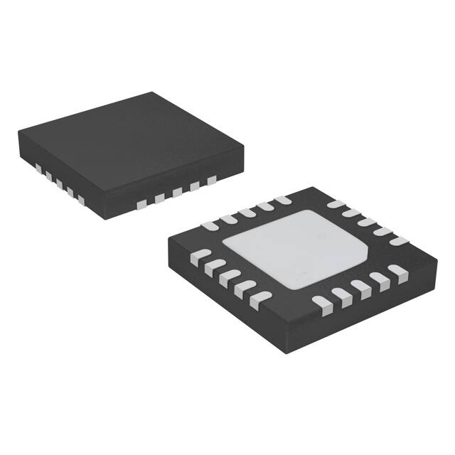
Uses compact package VQFN20 which makes it
suitable for mobile devices.
Single power supply of 3.3V
Output USB Clock
48.008022MHz
14.318182MHz
Output VIDEO Clock
17.734450MHz
Package
W(Typ) x D(Typ) x H(Max)
VQFN20
4.20mm x 4.20mm x 0.95mm
Applications
Generation of clocks used in digital still camera and
digital video camera systems
Typical Application Circuit
for Video
14.318182MHz
0.1µF
0.1uF
17.734450MHz
for USB
16:CLK2OUT
17:VSS2
1:AVDD
15:VDD1
2:AVDD
14:VDD1
0.1uF
0.1µF
0.1uF
0.1µF
BU2394KN
VQFN-20
3:AVSS
13:VSS1
10:FS1
11:CLK1OUT
9:FS2
5:XOUT
8:FS3
12:CLK2ON
7:XTAL_SEL
4:XIN
6:TEST1
R
18:VDD2
19:REF_CLK
20:TEST2
48.008022MHz
for CCD
135.000000MHz
110.000000MHz
108.000000MHz
98.181818MHz
(Note) We believe that this circuit is to be recommended. However, to use it, make further thorough check for the characteristics.
○Product structure:Silicon monolithic integrated circuit
www.rohm.com
© 2015 ROHM Co., Ltd. All rights reserved.
TSZ22111・14・001
○This product has no designed protection against radioactive rays
1/21
TSZ02201-0E3E0J500700-1-2
04.Nov.2015 Rev.001
�BU2394KN
Block Diagram and Pin Configuration
TOP VIEW
DATA
PLL1
XIN
4
XOUT
5
135.000000MHz
108.000000MHz
110.000000MHz
98.181818MHz
11
CLK1
16
CLK2
19
REF_CLK
XTAL
OSC
PLL2
48.008022MHz
1/4
1/2
XTAL_SEL
7
CLK2ON
12
FS1
10
FS2
9
FS3
8
PLL3
1/10
17.734450MHz
14.318182MHz
Pin Descriptions
Pin No.
1
2
3
4
5
6
7
8
9
10
11
12
13
14
15
16
17
18
19
20
Pin Name
AVDD
AVDD
AVSS
XIN
XOUT
TEST1
XTAL_SEL
FS3
FS2
FS1
CLK1OUT
CLK2ON
VSS1
VDD1
VDD1
CLK2OUT
VSS2
VDD2
REF_CLK
TEST2
Function
Analog power source
Analog power source
Analog GND
Crystal IN
Crystal OUT
TEST pin, normally open, equipped with pull-down
Crystal oscillator selection, H: 28.636 MHz, L: 14.318 MHz, equipped with pull-up
CLK1,2 output selection, equipped with pull-up
CLK1,2 output selection, equipped with pull-up
REFCLK output selection, equipped with pull-up
110M/98M/108M/135M output
CLK2 output control, H: Enable, L: Disable, equipped with pull-up
CLK1/CLK2 & Internal digital GND
CLK1/2 & Internal digital power supply
CLK1/2 & Internal digital power supply
48M output
REFCLK GND
REFCLK power supply
14.3M/17.7M output
TEST pin, normally open, equipped with pull-down
(Note) Basically, mount ICs to the printed circuit board for use.
If the ICs are not mounted to the printed circuit board, the characteristics of ICs may not be fully demonstrated.
Mount 0.1µF capacitors in the vicinity of the IC pins between PIN 1&2 and PIN 3, PIN 13 and PIN 14&15, and PIN 17 and PIN 18, respectively.
As to the jitters, the TYP values vary with the substrate, power supply, output loads, noises, and others. Also, the operating margin should be thoroughly
checked.
www.rohm.com
© 2015 ROHM Co., Ltd. All rights reserved.
TSZ22111・15・001
2/21
TSZ02201-0E3E0J500700-1-2
04.Nov.2015 Rev.001
�BU2394KN
Absolute Maximum Ratings (Ta=25°C)
Parameter
Symbol
Limit
Unit
VDD
-0.5 to +7.0
V
Input Voltage
VIN
-0.5 to VDD+0.5
V
Storage Temperature Range
Tstg
-30 to +125
°C
Pd
0.53(Note 1)
W
Supply Voltage
Power Dissipation
(Note 1) Derate by 5.3mW/°C when operating above Ta=25°C.
(Note) Operating temperature is not guaranteed.
(Note) Power dissipation is measured when the IC is mounted to the printed circuit board.
Caution: Operating the IC over the absolute maximum ratings may damage the IC. The damage can either be a short circuit between pins or an open circuit
between pins and the internal circuitry. Therefore, it is important to consider circuit protection measures, such as adding a fuse, in case the IC is operated over
the absolute maximum ratings.
Recommended Operating Conditions
Parameter
Symbol
Limit
Unit
Supply Voltage
VDD
3.0 to 3.6
V
Input H Voltage
VINH
0.8VDD to VDD
V
Input L Voltage
VINL
0.0 to 0.2VDD
V
Operating Temperature
Topr
-5 to +70
°C
CL
15(MAX)
pF
Output Load
www.rohm.com
© 2015 ROHM Co., Ltd. All rights reserved.
TSZ22111・15・001
3/21
TSZ02201-0E3E0J500700-1-2
04.Nov.2015 Rev.001
�BU2394KN
Electrical Characteristics
(VDD=3.3V, Ta=25°C, unless otherwise specified.)
When XTAL_SEL=H crystal frequency is 28.636363 MHz. At XTAL_SEL=L, crystal frequency is 14.318182 MHz
Parameter
Symbol
Operating Circuit Current
Limit
Unit
Conditions
Min
Typ
Max
IDD
-
45
60
mA
CLK1
VOH1
VDD-0.5
VDD-0.2
-
V
When current load = -9.0mA
CLK2
VOH2
VDD-0.5
VDD-0.2
-
V
When current load = -7.0mA
REF_CLK
VOHR
VDD-0.5
VDD-0.2
-
V
When current load = -4.5mA
CLK1
VOL1
-
0.2
0.5
V
When current load =11mA
CLK2
VOL2
-
0.2
0.5
V
When current load =9.0mA
REF_CLK
VOLR
-
0.2
0.5
V
When current load =5.5mA
Pull-Up
R
125
250
375
Ω
Monitor pin = 0V (R=VDD/I)
CLK1 FS2:H FS3:H
fCLK1-1
-
135.000000
-
MHz
XTAL x (1188/63)/2
CLK1 FS2:H FS3:L
fCLK1-2
-
108.000000
-
MHz
XTAL x (1056/70)/2
CLK1 FS2:L FS3:L
fCLK1-3
-
98.181818
-
MHz
XTAL x (864/63)/2
CLK1 FS2:L FS3:H
fCLK1-4
-
110.000000
-
MHz
XTAL x (968/63)/2
CLK2
fCLK2-2
-
48.008022
-
MHz
XTAL x (228/17)/4
REF_CLK FS1:H
fREF1-1
-
14.318182
-
MHz
XTAL Output
REF_CLK FS1:L
fREF1-2
-
17.734450
-
MHz
XTAL x (706/57)/10
At no load
【Output H Voltage】
【Output L Voltage】
【Pull-Up Resistance Value】
FS1, FS2, FS3,
CLK2ON, XTAL_SEL
【Output Frequency】
【Output Waveform】
Duty1
100MHz or Less
Duty1
45
50
55
%
Duty2
100MHz or More
Duty2
-
50
-
%
Rise Time
tR
-
2.5
-
nsec
Fall Time
tF
-
2.5
-
nsec
P-J1σ
P-J
MIN-MAX
tLOCK
-
30
-
psec
-
180
-
psec
-
-
1
msec
Measured at a voltage of 1/2
of VDD
Measured at a voltage of 1/2
of VDD
Period of transition time
required for the output to
reach 80% from 20% of VDD.
Period of transition time
required for the output to
reach 20% from 80% of VDD.
【Jitter】
Period-Jitter 1σ
Period-Jitter MIN-MAX
【Output Lock-Time】
(Note 1)
(Note 2)
(Note 3)
(Note) The output frequency is determined by the arithmetic (frequency division) expression of a frequency input to XTALIN. If the input frequency is set to values
shown below, the output frequency will be as listed above.
When XTAL_SEL is set to H, the input frequency on XTALIN will be 28.636363 MHz.
When XTAL_SEL is set to L, the input frequency on XTALIN will be 14.318182 MHz.
(Note 1) Period-Jitter 1σ
This parameter represents standard deviation (=1σ) on cycle distribution data at the time when the output clock cycles are sampled 1000 times consecutively
with the TDS7104 Digital Phosphor Oscilloscope of Tektronix Japan, Ltd.
(Note 2) Period-Jitter MIN-MAX
This parameter represents a maximum distribution width on cycle distribution data at the time when the output clock cycles are sampled 1000 times
consecutively with the TDS7104 Digital Phosphor Oscilloscope of Tektronix Japan, Ltd.
(Note 3) Output Lock-Time
The Lock-Time represents the elapsed time after power supply turns ON to reach a 3.0V voltage, after the system is switched from Power-Down state to
normal operation state, or after the output frequency is switched until it is stabilized at a specified frequency, respectively.
www.rohm.com
© 2015 ROHM Co., Ltd. All rights reserved.
TSZ22111・15・001
4/21
TSZ02201-0E3E0J500700-1-2
04.Nov.2015 Rev.001
�BU2394KN
Typical Performance Curves
1.0V/div
1.0V/div
(Basic Data)
1.0nsec/div
500psec/div
Figure 1. 135MHz Output Wave
(At VDD=3.3V and CL=15pF)
Figure 2. 135MHz Period-Jitter
(At VDD=3.3V and CL=15pF)
1.0V/div
10dB/div
RBW=1KHz
VBW=100Hz
10KHz/div
2.0nsec/div
Figure 3. 135MHz Spectrum
(At VDD=3.3V and CL=15pF)
www.rohm.com
© 2015 ROHM Co., Ltd. All rights reserved.
TSZ22111・15・001
Figure 4. 110MHz Output Wave
(At VDD=3.3V and CL=15pF)
5/21
TSZ02201-0E3E0J500700-1-2
04.Nov.2015 Rev.001
�BU2394KN
Typical Performance Curves – continued
1.0V/div
10dB/div
RBW=1KHz
VBW=100Hz
10KHz/div
500psec/div
Figure 6. 110MHz Spectrum
(At VDD=3.3V and CL=15pF)
1.0V/div
1.0V/div
Figure 5. 110MHz Period-Jitter
(At VDD=3.3V and CL=15pF)
2.0nsec/div
500psec/div
Figure 7. 108MHz Output Wave
(At VDD=3.3V and CL=15pF)
www.rohm.com
© 2015 ROHM Co., Ltd. All rights reserved.
TSZ22111・15・001
Figure 8. 108MHz Period-Jitter
(At VDD=3.3V and CL=15pF)
6/21
TSZ02201-0E3E0J500700-1-2
04.Nov.2015 Rev.001
�BU2394KN
Typical Performance Curves – continued
1.0V/div
10dB/div
RBW=1KHz
VBW=100Hz
10KHz/div
2.0nsec/div
Figure 10. 98MHz Output Wave
(At VDD=3.3V and CL=15pF)
Figure 9. 108MHz Spectrum
(At VDD=3.3V and CL=15pF)
1.0V/div
10dB/div
RBW=1KHz
VBW=100Hz
10KHz/div
500psec/div
Figure 12. 98MHz Spectrum
(At VDD=3.3V and CL=15pF)
Figure 11. 98MHz Period-Jitter
(At VDD=3.3V and CL=15pF)
www.rohm.com
© 2015 ROHM Co., Ltd. All rights reserved.
TSZ22111・15・001
7/21
TSZ02201-0E3E0J500700-1-2
04.Nov.2015 Rev.001
�BU2394KN
1.0V/div
1.0V/div
Typical Performance Curves – continued
5.0nsecdiv
500psec/div
Figure 13. 48MHz Output Wave
(At VDD=3.3V and CL=15pF)
Figure 14. 48MHz Period-Jitter
(At VDD=3.3V and CL=15pF)
10dB/div
1.0V/div
RBW=1KHz
VBW=100Hz
10.0nsec/div
10KHz/div
Figure 16. 17.7MHz Output Wave
(At VDD=3.3V and CL=15pF)
Figure 15. 48MHz Spectrum
(At VDD=3.3V and CL=15pF)
www.rohm.com
© 2015 ROHM Co., Ltd. All rights reserved.
TSZ22111・15・001
8/21
TSZ02201-0E3E0J500700-1-2
04.Nov.2015 Rev.001
�BU2394KN
Typical Performance Curves – continued
10dB/div
1.0V/div
RBW=1KHz
VBW=100Hz
10KHz/div
500psec/div
Figure 18. 17.7MHz Spectrum
(At VDD=3.3V and CL=15pF)
1.0V/div
1.0V/div
Figure 17. 17.7MHz Period-Jitter
(At VDD=3.3V and CL=15pF)
500psec/div
10.0nsec/div
Figure 19. 14.3MHz Output Wave
(At VDD=3.3V and CL=15pF)
www.rohm.com
© 2015 ROHM Co., Ltd. All rights reserved.
TSZ22111・15・001
Figure 20. 14.3MHz Period-Jitter
(At VDD=3.3V and CL=15pF)
9/21
TSZ02201-0E3E0J500700-1-2
04.Nov.2015 Rev.001
�BU2394KN
Typical Performance Curves – continued
10dB/div
RBW=1KHz
VBW=100Hz
10KHz/div
Figure 21. 14.3MHz Spectrum
(At VDD=3.3V and CL=15pF)
www.rohm.com
© 2015 ROHM Co., Ltd. All rights reserved.
TSZ22111・15・001
10/21
TSZ02201-0E3E0J500700-1-2
04.Nov.2015 Rev.001
�BU2394KN
Typical Performance Curves – continued
(Temperature and Supply voltage variations data)
100
54
90
Period-Jitter
P erio
[psec]
J-1 σ[psec]
d-ji tte r1 σ1σ::PPJ-1σ
55
: Duty[%]
Duty
Duty
: Duty [%]
53
52
51
50
VDD=2.9V
VDD=3.3V
VDD=3.7V
49
48
47
46
80
70
60
VDD=2.9V
VDD=3.3V
VDD=3.7V
50
40
30
20
10
0
45
-25
0
25
50
75
-25
100
0
Temperature : Ta [°C]
Temperature:T[℃]
75
100
Figure 23. Period-Jitter 1σ vs Temperature
(135MHz)
55
600
54
500
53
400
52
Duty::Duty[%]
Duty [%]
Duty
P erio d-ji tte rMIN-MA X:
50
Temperature : Ta [°C]
Temperature:T[℃]
Figure 22. Duty vs Temperature
(135MHz)
Period-Jitter
MIN-MAX :XPJ-MIN-MAX
[psec]
P J-MIN-MA
[p sec]
25
VDD=2.9V
300
VDD=3.3V
VDD=3.7V
200
51
50
VDD=2.9V
49
VDD=3.3V
48
VDD=3.7V
47
100
46
0
45
-25
0
25
50
75
100
-25
Temperature : Ta [°C]
Temperature:T[℃]
25
50
75
100
Temperature
: Ta [°C]
Temperature:T[℃]
Figure 24. Period-Jitter MIN-MAX vs Temperature
(135MHz)
www.rohm.com
© 2015 ROHM Co., Ltd. All rights reserved.
TSZ22111・15・001
0
Figure 25. Duty vs Temperature
(110MHz)
11/21
TSZ02201-0E3E0J500700-1-2
04.Nov.2015 Rev.001
�BU2394KN
90
80
P erio d-ji tte rMIN-MA X:
P erio
[psec]
J-1 σ
d-ji tte r1 σ
Period-Jitter
[psec]
1σ:: P
PJ-1σ
100
70
60
50
VDD=2.9V
40
VDD=3.3V
30
VDD=3.7V
20
10
0
-25
0
25
50
75
Period-Jitter
MIN-MAX :XPJ-MIN-MAX
[psec]
P J-MIN-MA
[p sec]
Typical Performance Curves – continued
600
500
400
300
VDD=2.9V
VDD=3.3V
200
VDD=3.7V
100
0
-25
100
0
Temperature : Ta [°C]
Temperature:T[℃]
54
90
52
51
50
VDD=2.9V
VDD=3.3V
VDD=3.7V
47
46
: P: PJ-1σ
P erioPeriod-Jitter
[psec]
J-1 σ [psec]
d-ji tte r1 σ1σ
100
53
: Duty[%]
Duty
: Duty [%]
Duty
75
100
Figure 27. Period-Jitter MIN-MAX vs Temperature
(110MHz)
55
48
50
Temperature : Ta [°C]
Temperature:T[℃]
Figure 26. Period-Jitter 1σ vs Temperature
(110MHz)
49
25
80
70
60
VDD=2.9V
50
VDD=3.3V
40
VDD=3.7V
30
20
10
0
45
-25
0
25
50
75
-25
100
25
50
75
100
Temperature : Ta [°C]
Temperature:T[℃]
Temperature : Ta [°C]
Temperature:T[℃]
Figure 29. Period-Jitter 1σ vs Temperature
(108MHz)
Figure 28. Duty vs Temperature
(108MHz)
www.rohm.com
© 2015 ROHM Co., Ltd. All rights reserved.
TSZ22111・15・001
0
12/21
TSZ02201-0E3E0J500700-1-2
04.Nov.2015 Rev.001
�BU2394KN
55
600
54
53
400
52
300
: Duty[%]
Duty
: Duty [%]
Duty
500
VDD=2.9V
VDD=3.3V
200
VDD=3.7V
100
50
49
VDD=2.9V
48
VDD=3.3V
VDD=3.7V
46
0
45
-25
0
25
50
75
100
-25
0
25
50
75
Temperature : Ta [°C]
Temperature:T[℃]
Temperature : Ta [°C]
Temperature:T[℃]
Figure 30. Period-Jitter MIN-MAX vs Temperature
(108MHz)
Figure 31. Duty vs Temperature
(98MHz)
100
P erio
[psec]
J-1 σ[psec]
d-ji tte r1 σ
Period-Jitter
1σ::PPJ-1σ
51
47
90
80
70
60
50
VDD=2.9V
40
VDD=3.3V
VDD=3.7V
30
20
10
0
-25
0
25
50
75
P erio d-ji tte rMIN-MA X:
Period-Jitter
MIN-MAX : PJ-MIN-MAX
[psec]
P J-MIN-MA
X [p sec]
P erio d-ji tte rMIN-MA X:
Period-Jitter
MIN-MAX : PJ-MIN-MAX
[psec]
P J-MIN-MA
X [p sec]
Typical Performance Curves – continued
Temperature
: Ta [°C]
Temperature:T[℃]
500
400
300
VDD=2.9V
200
VDD=3.7V
VDD=3.3V
100
0
0
25
50
75
100
Temperature : Ta [°C]
Temperature:T[℃]
Figure 32. Period-Jitter 1σ vs Temperature
(98MHz)
www.rohm.com
© 2015 ROHM Co., Ltd. All rights reserved.
TSZ22111・15・001
600
-25
100
100
Figure 33. Period-Jitter MIN-MAX vs Temperature
(98MHz)
13/21
TSZ02201-0E3E0J500700-1-2
04.Nov.2015 Rev.001
�BU2394KN
55
100
54
90
σ ::PJ-1σ
P erio
P J-1 σ
[psec]
d-ji tte r11σ
Period-Jitter
[psec]
: Duty[%]
: Duty [%]
Duty Duty
Typical Performance Curves – continued
53
52
51
50
49
VDD=2.9V
48
VDD=3.3V
47
VDD=3.7V
46
VDD=3.7V
80
VDD=3.3V
70
VDD=2.9V
60
50
40
30
20
10
0
45
-25
0
25
50
75
-25
100
0
Temperature : Ta [°C]
Temperature:T[℃]
75
100
Figure 35. Period-Jitter 1σ vs Temperature
(48MHz)
600
55
54
500
53
400
VDD=3.7V
300
VDD=2.9V
Duty :
: Duty
[%]
Duty
Duty[%]
P erio d-ji tte rMIN-MA X:
50
Temperature : Ta [°C]
Temperature:T[℃]
Figure 34. Duty vs Temperature
(48MHz)
Period-Jitter
MIN-MAX : PJ-MIN-MAX
[psec]
P J-MIN-MA
X [p sec]
25
VDD=3.3V
200
52
51
50
49
VDD=2.9V
48
VDD=3.3V
47
100
VDD=3.7V
46
45
0
-25
0
25
50
75
-25
100
0
25
50
75
Temperature
: Ta [°C]
Temperature:T[℃]
Temperature
: Ta [°C]
Temperature:T[℃]
Figure 36. Period-Jitter MIN-MAX vs Temperature
(98MHz)
Figure 37. Duty vs Temperature
(17.7MHz)
www.rohm.com
© 2015 ROHM Co., Ltd. All rights reserved.
TSZ22111・15・001
14/21
100
TSZ02201-0E3E0J500700-1-2
04.Nov.2015 Rev.001
�BU2394KN
Typical Performance Curves – continued
P erio d-ji tte rMIN-MA X:
Period-Jitter
: PJ-MIN-MAX
P MIN-MAX
J-MIN-MA
X [p sec] [psec]
Period-Jitter
[psec]
1σ :: P
PJ-1σ
P erio
[psec]
J-1 σ
d-ji tte r1 σ
100
90
80
VDD=3.7V
70
VDD=3.3V
60
VDD=2.9V
50
40
30
20
10
0
-25
0
25
50
75
600
500
VDD=3.7V
400
VDD=3.3V
VDD=2.9V
300
200
100
0
100
-25
0
Figure 38. Period-Jitter 1σ vs Temperature
(17.7MHz)
54
90
Period-Jitter
1σ::PPJ-1σ
P erio
[psec]
J-1 σ[psec]
d-ji tte r1 σ
100
Duty::Duty[%]
Duty [%]
Duty
53
52
51
50
49
47
VDD=3.3V
VDD=3.7V
46
75
100
Figure 39. Period-Jitter MIN-MAX vs Temperature
(17.7MHz)
55
VDD=2.9V
50
Temperature : Ta [°C]
Temperature:T[℃]
Temperature:T[℃]
Temperature : Ta [°C]
48
25
80
VDD=3.7V
70
VDD=3.3V
60
VDD=2.9V
50
40
30
20
10
0
45
-25
0
25
50
75
-25
100
25
50
75
100
Temperature:T[℃]
Temperature
: Ta [°C]
Temperature
: Ta [°C]
Temperature:T[℃]
Figure 41. Period-Jitter 1σ vs Temperature
(14.3MHz)
Figure 40. Duty vs Temperature
(14.3MHz)
www.rohm.com
© 2015 ROHM Co., Ltd. All rights reserved.
TSZ22111・15・001
0
15/21
TSZ02201-0E3E0J500700-1-2
04.Nov.2015 Rev.001
�BU2394KN
600
60
:IDD[mA
Operating
Circuit
Current:]IDD [mA]
IDD
P erio d-ji tte rMIN-MA X:
Period-Jitter
MIN-MAX :X
[psec]
PJ-MIN-MAX
P J-MIN-MA
[p sec]
Typical Performance Curves – continued
500
400
VDD=3.7V
VDD=3.3V
300
VDD=2.9V
200
100
50
40
VDD=3.7V
30
VDD=3.3V
VDD=2.9V
20
10
0
0
-25
0
25
50
75
100
0
25
50
75
100
Temperature:T[℃]
Temperature : Ta [°C]
Temperature:T[℃]
Temperature : Ta [°C]
Figure 43. Operating Circuit Current vs Temperature
(At 1chip operation)
Figure 42. Period-Jitter MIN-MAX vs Temperature
(14.3MHz)
www.rohm.com
© 2015 ROHM Co., Ltd. All rights reserved.
TSZ22111・15・001
-25
16/21
TSZ02201-0E3E0J500700-1-2
04.Nov.2015 Rev.001
�BU2394KN
Operational Notes
1.
Reverse Connection of Power Supply
Connecting the power supply in reverse polarity can damage the IC. Take precautions against reverse polarity when
connecting the power supply, such as mounting an external diode between the power supply and the IC’s power
supply pins.
2.
Power Supply Lines
Design the PCB layout pattern to provide low impedance supply lines. Separate the ground and supply lines of the
digital and analog blocks to prevent noise in the ground and supply lines of the digital block from affecting the analog
block. Furthermore, connect a capacitor to ground at all power supply pins. Consider the effect of temperature and
aging on the capacitance value when using electrolytic capacitors.
3.
Ground Voltage
Ensure that no pins are at a voltage below that of the ground pin at any time, even during transient condition.
4.
Ground Wiring Pattern
When using both small-signal and large-current ground traces, the two ground traces should be routed separately but
connected to a single ground at the reference point of the application board to avoid fluctuations in the small-signal
ground caused by large currents. Also ensure that the ground traces of external components do not cause variations
on the ground voltage. The ground lines must be as short and thick as possible to reduce line impedance.
5.
Thermal Consideration
Should by any chance the power dissipation rating be exceeded the rise in temperature of the chip may result in
deterioration of the properties of the chip. In case of exceeding this absolute maximum rating, increase the board size
and copper area to prevent exceeding the Pd rating.
6.
Recommended Operating Conditions
These conditions represent a range within which the expected characteristics of the IC can be approximately obtained.
The electrical characteristics are guaranteed under the conditions of each parameter.
7.
Inrush Current
When power is first supplied to the IC, it is possible that the internal logic may be unstable and inrush current may flow
instantaneously due to the internal powering sequence and delays, especially if the IC has more than one power
supply. Therefore, give special consideration to power coupling capacitance, power wiring, width of ground wiring, and
routing of connections.
8.
Operation Under Strong Electromagnetic Field
Operating the IC in the presence of a strong electromagnetic field may cause the IC to malfunction.
9.
Testing on Application Boards
When testing the IC on an application board, connecting a capacitor directly to a low-impedance output pin may
subject the IC to stress. Always discharge capacitors completely after each process or step. The IC’s power supply
should always be turned off completely before connecting or removing it from the test setup during the inspection
process. To prevent damage from static discharge, ground the IC during assembly and use similar precautions during
transport and storage.
10. Inter-pin Short and Mounting Errors
Ensure that the direction and position are correct when mounting the IC on the PCB. Incorrect mounting may result in
damaging the IC. Avoid nearby pins being shorted to each other especially to ground, power supply and output pin.
Inter-pin shorts could be due to many reasons such as metal particles, water droplets (in very humid environment) and
unintentional solder bridge deposited in between pins during assembly to name a few.
11. Unused Input Pins
Input pins of an IC are often connected to the gate of a MOS transistor. The gate has extremely high impedance and
extremely low capacitance. If left unconnected, the electric field from the outside can easily charge it. The small charge
acquired in this way is enough to produce a significant effect on the conduction through the transistor and cause
unexpected operation of the IC. So unless otherwise specified, unused input pins should be connected to the power
supply or ground line.
www.rohm.com
© 2015 ROHM Co., Ltd. All rights reserved.
TSZ22111・15・001
17/21
TSZ02201-0E3E0J500700-1-2
04.Nov.2015 Rev.001
�BU2394KN
Operational Notes – continued
12. Regarding the Input Pin of the IC
In the construction of this IC, P-N junctions are inevitably formed creating parasitic diodes or transistors. The operation
of these parasitic elements can result in mutual interference among circuits, operational faults, or physical damage.
Therefore, conditions which cause these parasitic elements to operate, such as applying a voltage to an input pin
lower than the ground voltage should be avoided. Furthermore, do not apply a voltage to the input pins when no power
supply voltage is applied to the IC. Even if the power supply voltage is applied, make sure that the input pins have
voltages within the values specified in the electrical characteristics of this IC.
13. Ceramic Capacitor
When using a ceramic capacitor, determine the dielectric constant considering the change of capacitance with
temperature and the decrease in nominal capacitance due to DC bias and others.
www.rohm.com
© 2015 ROHM Co., Ltd. All rights reserved.
TSZ22111・15・001
18/21
TSZ02201-0E3E0J500700-1-2
04.Nov.2015 Rev.001
�BU2394KN
Ordering Information
B
U
2
3
9
4
Part Number
K
N
-
Package
KN: VQFN20
E2
Package and forming specification
E2: Reel-like emboss taping
Marking Diagram
VQFN20 (TOP VIEW)
Part Number Marking
U2394K
LOT Number
1PIN MARK
www.rohm.com
© 2015 ROHM Co., Ltd. All rights reserved.
TSZ22111・15・001
19/21
TSZ02201-0E3E0J500700-1-2
04.Nov.2015 Rev.001
�BU2394KN
Physical Dimension, Tape and Reel Information
Package Name
VQFN20
(unit:mm)
Caution)Don’t recommended soldering at corner
< Tape and Reel Information >
Tape
Embossed carrier tape with dry pack
Quantity 2500pcs
Direction
E2
of feed
The direction is the pin 1 of product is at the upper left when you hold
reel on the left hand and you pull out the tape on the right hand
www.rohm.com
© 2015 ROHM Co., Ltd. All rights reserved.
TSZ22111・15・001
20/21
TSZ02201-0E3E0J500700-1-2
04.Nov.2015 Rev.001
�BU2394KN
Revision History
Date
Revision
04.Nov.2015
001
Changes
New Release
www.rohm.com
© 2015 ROHM Co., Ltd. All rights reserved.
TSZ22111・15・001
21/21
TSZ02201-0E3E0J500700-1-2
04.Nov.2015 Rev.001
�Datasheet
Notice
Precaution on using ROHM Products
1.
Our Products are designed and manufactured for application in ordinary electronic equipments (such as AV equipment,
OA equipment, telecommunication equipment, home electronic appliances, amusement equipment, etc.). If you
(Note 1)
, transport
intend to use our Products in devices requiring extremely high reliability (such as medical equipment
equipment, traffic equipment, aircraft/spacecraft, nuclear power controllers, fuel controllers, car equipment including car
accessories, safety devices, etc.) and whose malfunction or failure may cause loss of human life, bodily injury or
serious damage to property (“Specific Applications”), please consult with the ROHM sales representative in advance.
Unless otherwise agreed in writing by ROHM in advance, ROHM shall not be in any way responsible or liable for any
damages, expenses or losses incurred by you or third parties arising from the use of any ROHM’s Products for Specific
Applications.
(Note1) Medical Equipment Classification of the Specific Applications
JAPAN
USA
EU
CHINA
CLASSⅢ
CLASSⅡb
CLASSⅢ
CLASSⅢ
CLASSⅣ
CLASSⅢ
2.
ROHM designs and manufactures its Products subject to strict quality control system. However, semiconductor
products can fail or malfunction at a certain rate. Please be sure to implement, at your own responsibilities, adequate
safety measures including but not limited to fail-safe design against the physical injury, damage to any property, which
a failure or malfunction of our Products may cause. The following are examples of safety measures:
[a] Installation of protection circuits or other protective devices to improve system safety
[b] Installation of redundant circuits to reduce the impact of single or multiple circuit failure
3.
Our Products are designed and manufactured for use under standard conditions and not under any special or
extraordinary environments or conditions, as exemplified below. Accordingly, ROHM shall not be in any way
responsible or liable for any damages, expenses or losses arising from the use of any ROHM’s Products under any
special or extraordinary environments or conditions. If you intend to use our Products under any special or
extraordinary environments or conditions (as exemplified below), your independent verification and confirmation of
product performance, reliability, etc, prior to use, must be necessary:
[a] Use of our Products in any types of liquid, including water, oils, chemicals, and organic solvents
[b] Use of our Products outdoors or in places where the Products are exposed to direct sunlight or dust
[c] Use of our Products in places where the Products are exposed to sea wind or corrosive gases, including Cl2,
H2S, NH3, SO2, and NO2
[d] Use of our Products in places where the Products are exposed to static electricity or electromagnetic waves
[e] Use of our Products in proximity to heat-producing components, plastic cords, or other flammable items
[f] Sealing or coating our Products with resin or other coating materials
[g] Use of our Products without cleaning residue of flux (even if you use no-clean type fluxes, cleaning residue of
flux is recommended); or Washing our Products by using water or water-soluble cleaning agents for cleaning
residue after soldering
[h] Use of the Products in places subject to dew condensation
4.
The Products are not subject to radiation-proof design.
5.
Please verify and confirm characteristics of the final or mounted products in using the Products.
6.
In particular, if a transient load (a large amount of load applied in a short period of time, such as pulse. is applied,
confirmation of performance characteristics after on-board mounting is strongly recommended. Avoid applying power
exceeding normal rated power; exceeding the power rating under steady-state loading condition may negatively affect
product performance and reliability.
7.
De-rate Power Dissipation depending on ambient temperature. When used in sealed area, confirm that it is the use in
the range that does not exceed the maximum junction temperature.
8.
Confirm that operation temperature is within the specified range described in the product specification.
9.
ROHM shall not be in any way responsible or liable for failure induced under deviant condition from what is defined in
this document.
Precaution for Mounting / Circuit board design
1.
When a highly active halogenous (chlorine, bromine, etc.) flux is used, the residue of flux may negatively affect product
performance and reliability.
2.
In principle, the reflow soldering method must be used on a surface-mount products, the flow soldering method must
be used on a through hole mount products. If the flow soldering method is preferred on a surface-mount products,
please consult with the ROHM representative in advance.
For details, please refer to ROHM Mounting specification
Notice-PGA-E
© 2015 ROHM Co., Ltd. All rights reserved.
Rev.002
�Datasheet
Precautions Regarding Application Examples and External Circuits
1.
If change is made to the constant of an external circuit, please allow a sufficient margin considering variations of the
characteristics of the Products and external components, including transient characteristics, as well as static
characteristics.
2.
You agree that application notes, reference designs, and associated data and information contained in this document
are presented only as guidance for Products use. Therefore, in case you use such information, you are solely
responsible for it and you must exercise your own independent verification and judgment in the use of such information
contained in this document. ROHM shall not be in any way responsible or liable for any damages, expenses or losses
incurred by you or third parties arising from the use of such information.
Precaution for Electrostatic
This Product is electrostatic sensitive product, which may be damaged due to electrostatic discharge. Please take proper
caution in your manufacturing process and storage so that voltage exceeding the Products maximum rating will not be
applied to Products. Please take special care under dry condition (e.g. Grounding of human body / equipment / solder iron,
isolation from charged objects, setting of Ionizer, friction prevention and temperature / humidity control).
Precaution for Storage / Transportation
1.
Product performance and soldered connections may deteriorate if the Products are stored in the places where:
[a] the Products are exposed to sea winds or corrosive gases, including Cl2, H2S, NH3, SO2, and NO2
[b] the temperature or humidity exceeds those recommended by ROHM
[c] the Products are exposed to direct sunshine or condensation
[d] the Products are exposed to high Electrostatic
2.
Even under ROHM recommended storage condition, solderability of products out of recommended storage time period
may be degraded. It is strongly recommended to confirm solderability before using Products of which storage time is
exceeding the recommended storage time period.
3.
Store / transport cartons in the correct direction, which is indicated on a carton with a symbol. Otherwise bent leads
may occur due to excessive stress applied when dropping of a carton.
4.
Use Products within the specified time after opening a humidity barrier bag. Baking is required before using Products of
which storage time is exceeding the recommended storage time period.
Precaution for Product Label
QR code printed on ROHM Products label is for ROHM’s internal use only.
Precaution for Disposition
When disposing Products please dispose them properly using an authorized industry waste company.
Precaution for Foreign Exchange and Foreign Trade act
Since concerned goods might be fallen under listed items of export control prescribed by Foreign exchange and Foreign
trade act, please consult with ROHM in case of export.
Precaution Regarding Intellectual Property Rights
1.
All information and data including but not limited to application example contained in this document is for reference
only. ROHM does not warrant that foregoing information or data will not infringe any intellectual property rights or any
other rights of any third party regarding such information or data.
2.
ROHM shall not have any obligations where the claims, actions or demands arising from the combination of the
Products with other articles such as components, circuits, systems or external equipment (including software).
3.
No license, expressly or implied, is granted hereby under any intellectual property rights or other rights of ROHM or any
third parties with respect to the Products or the information contained in this document. Provided, however, that ROHM
will not assert its intellectual property rights or other rights against you or your customers to the extent necessary to
manufacture or sell products containing the Products, subject to the terms and conditions herein.
Other Precaution
1.
This document may not be reprinted or reproduced, in whole or in part, without prior written consent of ROHM.
2.
The Products may not be disassembled, converted, modified, reproduced or otherwise changed without prior written
consent of ROHM.
3.
In no event shall you use in any way whatsoever the Products and the related technical information contained in the
Products or this document for any military purposes, including but not limited to, the development of mass-destruction
weapons.
4.
The proper names of companies or products described in this document are trademarks or registered trademarks of
ROHM, its affiliated companies or third parties.
Notice-PGA-E
© 2015 ROHM Co., Ltd. All rights reserved.
Rev.002
�Datasheet
General Precaution
1. Before you use our Pro ducts, you are requested to care fully read this document and fully understand its contents.
ROHM shall n ot be in an y way responsible or liabl e for fa ilure, malfunction or acci dent arising from the use of a ny
ROHM’s Products against warning, caution or note contained in this document.
2. All information contained in this docume nt is current as of the issuing date and subj ect to change without any prior
notice. Before purchasing or using ROHM’s Products, please confirm the la test information with a ROHM sale s
representative.
3.
The information contained in this doc ument is provi ded on an “as is” basis and ROHM does not warrant that all
information contained in this document is accurate an d/or error-free. ROHM shall not be in an y way responsible or
liable for an y damages, expenses or losses incurred b y you or third parties resulting from inaccur acy or errors of or
concerning such information.
Notice – WE
© 2015 ROHM Co., Ltd. All rights reserved.
Rev.001
�