物料型号:
- 型号:BU2879AK
器件简介:
- BU2879AK是一款用于荧光显示器的驱动IC。它配备了26个耐高压输出,能够显示从11个15字符到16个8字符的显示内容。该IC还具备按键扫描功能和通用输入引脚,非常适合用于VTR等设备的前面板。通过串行接口,可以从微计算机控制其功能。
引脚分配:
- VDD(14,38):电源引脚1,连接到系统电源。
- OSC(44):振荡引脚,用于振荡的电容器连接引脚。
- Vss(7,43):地引脚,连接到系统地。
- SI(6):串行数据输入,从MSB开始的串行数据输入。
- SO(5):串行数据输出,从MSB开始的串行数据输出;Nch开漏输出。
- SCK(8):串行时钟输入,串行数据在上升沿读取。
- CS(9):串行芯片选择,当为低时进行串行初始化,在高时有效。
- S1~S11(15~25):用于段的耐高压输出引脚,Pch开漏输出+下拉电阻。
- VEE(27):电源引脚2,用于FLP驱动输出的下拉电阻连接。
- G1~G10(42~39, 37~32):用于栅格的耐高压输出引脚,Pch开漏输出+下拉电阻。
- S12/G15、S16/G11(26, 28~31):用于段/栅格的耐高压输出引脚,用于在段和栅格输出之间切换;Pch开漏输出+下拉电阻。
- K1~K4(10~13):按键数据输入引脚,用于按键扫描的数据输入引脚。
- SW1~SW4(1~4):通用输入引脚,通用输入引脚;输入数据可以串行传输到微计算机。
参数特性:
- 工作电压:VDD(4.5~5.5V),VEE(VDD-37V到VDD-0V)。
- 耐压:VDD(-0.3V到+7.0V),VEE(VD+0.3V到VDD-40V)。
- 输入电压:VIN(-0.3V到VDD+0.3V)。
- 功耗:Pd(850mW,注意:功耗随温度升高而降低)。
- 工作温度:Topr(-25~+75°C),存储温度:Tstg(-55~+125°C)。
功能详解:
- 1) 高耐压输出。
- 2) 显示模式:11S × 15G ~ 16S × 8G。
- 3) 可变显示亮度(7级)。
- 4) 3线串行接口。
- 5) 按键扫描功能(6×4)。
- 6) 内部下拉电阻(耐高压输出)。
- 7) QFP 44封装。
应用信息:
- 应用于VCRs等设备。
封装信息:
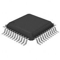
- QFP 44封装。