Datasheet
CMOS LDO Regulators for Portable Equipments
1ch 500mA
CMOS LDO Regulators
BUxxSA5WGWZ series
●General Description
BUxxSA5WGWZ series are high-performance CMOS LDO
regulators with output current ability of up to 500-mA.
These devices have excellent noise and load response
characteristics despite of its low circuit current
consumption of 33µA. They are most appropriate for
various applications such as power supplies for logic IC,
RF, and camera modules.
●Key Specifications
Input Power Supply Voltage Range:
1.8V to 5.0V
Output Current Range:
0mA to 500mA
Operating Temperature Range:
-40℃ to +105℃
Output Voltage Lineup:
3.0V,3.3V
Output Voltage Accuracy:
±1.0%
Circuit Current:
33µA(Typ.)
Standby Current:
0μA (Typ.)
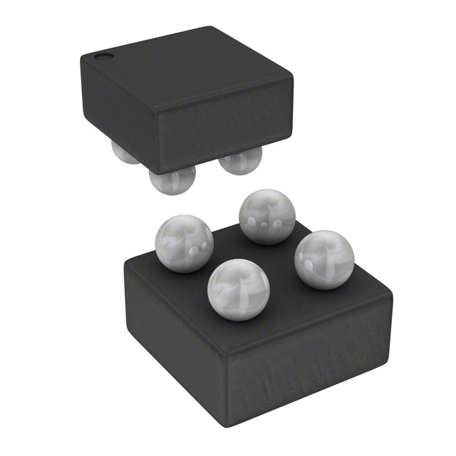
●Package
W(Typ.) x D(Typ.) x H(Max.)
UCSP30L1(BUXXSA5WGWZ)
0.8mm x 0.8mm x 0.33mm
●Features
High Output Voltage Accuracy: ±1.0%
High Ripple Rejection: 70 dB (Typ, 1 kHz,)
Compatible with small ceramic capacitor
(Cin=Cout=0.47 µF)
Low Current Consumption: 33µA
Output Voltage ON/OFF control
Built-in Over Current Protection Circuit (OCP)
Built-in Thermal Shutdown Circuit (TSD)
Adopting ultra-small WLCSP UCSP30L1
●Applications
Portable devices
Camera modules
Other electronic devices using microcontrollers or
logic circuits
●Typical Application Circuit
Vin
VOUT
VIN
Cin
Vout
Cout
BUxxSD2MG-M
BUxxSA5WGWZ
On
Off
STBY
GND
Figure 1. Typical Application Circuit
○Product structure:Silicon monolithic integrated circuit
.www.rohm.com
© 2012 ROHM Co., Ltd. All rights reserved.
TSZ22111・14・001
○This product is not designed protection against radioactive rays
1/16
TSZ02201-0RBR0GZ00120-1-2
2013.05.09 Rev.001
�Datasheet
BUxxSA5WGWZ series
●Pin Configuration
1Pin Mark
1
2
A
B
Top View
(Mark Side)
B
A
1
2
Bottom View
●Pin Description
Pin No.
Symbol
Function
A1
GND
GND Pin
A2
STBY
Output Control Pin
(High:ON, Low:OFF)
B1
VOUT
Output Pin
B2
VIN
Input Pin
●Block Diagram
VIN
VIN
B2
VREF
Cin
GND
A1
+
OCP
VOUT
VOUT
B1
Cout
TSD
VSTBY
STBY
A2
STBY
Cin(min)=0.47µF (Ceramic)
Cout(min)=0.47µF (Ceramic)
Figure 2. Block diagram
www.rohm.com
© 2012 ROHM Co., Ltd. All rights reserved.
TSZ22111・15・001
2/16
TSZ02201-0RBR0GZ00120-1-2
2013.05.09 Rev.001
�Datasheet
BUxxSA5WGWZ series
●Absolute Maximum Ratings
Parameter
Symbol
Rating
Unit
VMAX
-0.3 to +5.5
V
Power Dissipation
Pd
410(*1)
mW
Maximum Junction
Temperature
Tjmax
+125
℃
Operating Temperature Range
Topr
-40 to +105
℃
Storage Temperature Range
Tstg
-55 to +125
℃
Power Supply Voltage
(*1)
Derate by 4.1mW/℃ when operating above Ta=25℃.(When mounted on a board 63mm×55mm×1.6mm glass-epoxy board, 9 layer)
●Recommended Operating Ratings
Parameter
Symbol
Limit
Unit
VIN
1.8 to 5.0
V
Input Power Supply Voltage
Range
●Recommended Operating Conditions
Parameter
Symbol
Input capacitor
Output capacitor
Rating
Unit
Conditions
-
µF
A ceramic capacitor is recommended.
-
µF
A ceramic capacitor is recommended.
Min.
Typ.
Max.
Cin
0.47(*2)
1.0
Cout
0.47(*2)
1.0
(*2) Set the value of the capacitor so that it does not fall below the minimum value. Take into consideration the temperature characteristics,
DC device characteristics, and degradation with time.
www.rohm.com
© 2012 ROHM Co., Ltd. All rights reserved.
TSZ22111・15・001
3/16
TSZ02201-0RBR0GZ00120-1-2
2013.05.09 Rev.001
�Datasheet
BUxxSA5WGWZ series
●Electrical Characteristics
(*6)
(Unless otherwise noted, Ta=-25℃, VIN=VOUT+1.0V , VSTBY=1.5V, Cin=1μF, Cout=1μF.)
Limit
PARAMETER
Symbol
Unit
MIN.
TYP.
MAX.
Conditions
Output Voltage 1
VOUT1
VOUT
×0.99
VOUT
VOUT
×1.01
V
IOUT = 10μA, VOUT≧2.5V
Output Voltage 2
VOUT2
VOUT
-25mV
VOUT
VOUT
+25mV
V
IOUT=10μA, VOUT<2.5V
Circuit Current
Circuit Current (STBY)
Ripple Rejection Ratio
IGND
ICCST
RR
-
33
70
80
1.0
-
μA
μA
dB
Dropout Voltage
VDROP
-
80
150
mV
IOUT=0mA
STBY=0V
VRR=-20dBv,fRR=1kHz,IOUT=10mA
VIN=0.98×VOUT, IOUT=100mA
Ta=-40 to +85℃(*4), VOUT≧2.5V
Line Regulation
VDLI
-
2
8
mV
IOUT=10μA VIN=VOUT+0.5 to 5.0V(*5)
Load Regulation1
VDLO1
-
6
45
mV
IOUT=0.01 to 300mA(*6)
Load Regulation2
STBY Pin Current
STBY Control
Voltage
VDLO2
ISTBY
VSTBH
VSTBL
1.2
-0.2
10
-
55
4.0
VIN
0.3
mV
μA
V
V
IOUT=0.01 to 500mA(*6)
ON
OFF
Ta=-40 to +85℃
(*3) VIN=3.5V for VOUT<2.5V.
(*4) Typical values apply for Ta=25℃.
(*5) VIN=3.0V to 5.0V for VOUT<2.5V.
(*6) Operating conditions are limited by Pd.
www.rohm.com
© 2012 ROHM Co., Ltd. All rights reserved.
TSZ22111・15・001
4/16
TSZ02201-0RBR0GZ00120-1-2
2013.05.09 Rev.001
�Datasheet
BUxxSA5WGWZ series
●Reference data BU33SA5WGWZ
(Unless otherwise specified, Ta=25℃.)
3.5
3.40
Temp=25°C
VIN=STBY
3.0
Temp=25°C
VIN=STBY
3.38
3.36
Output Voltage (V)
Output Voltage (V)
2.5
2.0
1.5
1.0
IOUT=0uA
IOUT=50mA
IOUT=200mA
0.5
3.34
3.32
3.30
IOUT=0uA
IOUT=50mA
IOUT=200mA
3.28
3.26
3.24
3.22
0.0
3.20
0
0.5 1
1.5 2 2.5 3 3.5 4
Input Voltage (V)
4.5 5
0
5.5
0.5
1.5
2
2.5
3
3.5
4
4.5
5
5.5
Input Voltage (V)
Figure 3. Output Voltage vs. Input Voltage
Figure 4. Line Regulation
100
3.40
VIN=STBY
IOUT=0uA
3.38
80
VIN=4.3V
STBY=1.5V
3.36
Output Voltage (V)
GND Current (uA)
1
Temp=-40°C
Temp=25°C
Temp=85°C
60
40
3.34
3.32
Temp=25°C
3.30
3.28
Temp=-40°C
3.26
Temp=85°C
3.24
20
3.22
3.20
0
0
0.5
1
1.5
2
2.5
3
3.5
4
4.5
5
0
5.5
100
150
200
Output Current (mA)
Input Voltage (V)
Figure 5. GND Current vs. Input Voltage
www.rohm.com
© 2012 ROHM Co., Ltd. All rights reserved.
TSZ22111・15・001
50
Figure 6. Load Regulation
5/16
TSZ02201-0RBR0GZ00120-1-2
2013.05.09 Rev.001
�Datasheet
BUxxSA5WGWZ series
●Reference data BU33SA5WGWZ
(Unless otherwise specified, Ta=25℃.)
120
3.5
Temp=85°C
3.0
Output voltage (V)
GND Current (µA)
100
Temp=25°C
80
60
40
Temp=-40°C
20
2.5
VIN=3.7V
VIN=4.3V
2.0
VIN=5.5V
1.5
1.0
0.5
0
0
50
100
150
0.0
200
0
100
200
Output Current (mA)
400
500
600
700
800
Output Current (mA)
Figure 8. OCP Threshold
Figure 7. GND Current vs. Output Current
3.40
60
VIN=4.3V
STBY=1.5V
IOUT=0.1mA
3.38
3.36
50
3.34
GND Current (µA)
Output Voltage (V)
300
3.32
3.30
3.28
3.26
3.24
40
30
VIN=4.3V
STBY=1.5V
IOUT=0.1m A
20
10
3.22
3.20
-40
-15
10
35
60
0
-40
85
Temperature (°C)
10
35
60
85
Temperature (°C)
Figure 9. Output Voltage vs. Temperature
www.rohm.com
© 2012 ROHM Co., Ltd. All rights reserved.
TSZ22111・15・001
-15
Figure 10. GND Current vs. Temperature
6/16
TSZ02201-0RBR0GZ00120-1-2
2013.05.09 Rev.001
�Datasheet
BUxxSA5WGWZ series
●Reference data BU33SA5WGWZ
(Unless otherwise specified, Ta=25℃.)
100
3.5
80
GND Current (at STBY) (nA)
3.0
Output Voltage (V)
90
VIN=4.3V
IOUT=0.1m A
Tem p=-40°C
2.5
Tem p=25°C
2.0
Tem p=85°C
1.5
1.0
0.5
0.0
0
0.25
0.5
0.75
1
1.25
VIN=5.5V
STBY=0V
70
60
50
40
30
20
10
0
-40
1.5
-15
Figure 11. STBY Threshold
60
85
Figure 12. GND Current (at STBY) vs. Temperature
1.6
200
1.4
180
VIN=0.98×VO UT
STBY=1.5V
160
1.2
Dropout VOUT [V]
STBY Pin Current (µA)
35
Temperature (°C)
STBY Voltage (V)
1.0
0.8
0.6
Tem p=-40°C
Tem p=25°C
Tem p=85°C
0.4
10
Tem p=85°C
140
Tem p=25°C
120
Tem p=-40°C
100
80
60
40
0.2
20
0.0
0
0
0.5
1
1.5
2
2.5
3
3.5
4
4.5
5
5.5
0
STBY Voltage (V)
100
150
200
Output Current (mA)
Figure 13. STBY Pin Current vs. STBY Voltage
www.rohm.com
© 2012 ROHM Co., Ltd. All rights reserved.
TSZ22111・15・001
50
Figure 14. Dropout Voltage vs. Output Current
7/16
TSZ02201-0RBR0GZ00120-1-2
2013.05.09 Rev.001
�Datasheet
BUxxSA5WGWZ series
80
80
70
70
Ripple Rejection (dB)
Ripple Rejection (dB)
●Reference data BU33SA5WGWZ (Unless otherwise specified, Ta=25℃,Cin = Cout =1μF.)
60
50
40
30
Ta = 25℃
Iout = 10mA
VIN_AC = -20dBV
20
10
Ta = 25℃
Iout = 10mA
60
50
40
30
20
10
0
3.3
3.8
4.3
4.8
0
100
5.3
Input Voltage (V)
1000
10000
100000
Frequency (Hz)
Figure 15. Ripple Rejection vs. Input Voltage
Figure 16. Ripple Rejection vs. Frequency
70
10
Output Noise Density (uV / √Hz)
Output Noise (uVrms)
60
50
40
30
20
Ta = 25℃
Vin = 4.3V
10
1
0.1
0.01
0
0
50
100
150
10
200
Output Current (mA)
1000
10000
100000
Frequency (Hz)
Figure 18. Output Noise Density vs. Frequency
Figure 17. Output Noise vs. Output Current
www.rohm.com
© 2012 ROHM Co., Ltd. All rights reserved.
TSZ22111・15・001
100
8/16
TSZ02201-0RBR0GZ00120-1-2
2013.05.09 Rev.001
�Datasheet
BUxxSA5WGWZ series
●Reference data BU33SA5WGWZ (Unless otherwise specified, Ta=25℃,Cin = Cout =1μF.)
1.0
0.0
2.0
20us/div
Cout=0.47uF
Cout=1uF
Cout=2.2uF
1.0
0.0
Output Volatage(V)
Output Volatage(V)
3.0
VOUT
VOUT
2.0
1V/div
VIN=4.3V
1.0
0.0
0.0
1.0
400ms/div
VOUT
0.0
20us/div
3.0
Cout=0.47uF
Cout=1uF
Cout=2.2uF
1V/div
0.0
VIN=4.3V
Output Volatage(V)
Output Volatage(V)
1V/div
STBY=1.5V→0V
STBY Voltage(V)
1V/div
2.0
3.0
1.0
VIN=4.3V
STBY Voltage(V)
1.0
2.0
1V/div
Cout=0.47uF
Cout=1uF
Cout=2.2uF
Figure 20. Startup time ( Rout = 16.5 ohm )
2.0
VOUT
VOUT
2.0
Figure 19. Startup time ( Rout = none )
STBY=1.5V→0V
1.0
0.0
20us/div
3.0
1V/div
STBY=0V→1.5V
STBY Voltage(V)
1V/div
STBY=0V→1.5V
STBY Voltage(V)
2.0
Figure 21. Discharge time ( Rout = none )
www.rohm.com
© 2012 ROHM Co., Ltd. All rights reserved.
TSZ22111・15・001
2.0
1.0
Cout=0.47uF
Cout=1uF
Cout=2.2uF
1V/div
0.0
VIN=4.3V
Figure 22. Discharge time ( Rout = 16.5 ohm )
9/16
TSZ02201-0RBR0GZ00120-1-2
2013.05.09 Rev.001
�Datasheet
BUxxSA5WGWZ series
●Reference data BU33SA5WGWZ (Unless otherwise specified, Ta=25℃,Cin = Cout =1μF.)
VIN=4.3V
STBY=4.3V
Cout=1uF
IOUT=1mA→150mA
100
100mA/div
VIN=4.3V
STBY=4.3V
Cout=1uF
3.40
2.0us/div
3.30
3.25
VOUT 50mV/div
3.20
2.0us/div
3.35
VOUT
3.30
Figure 24. Load response
( Iout = 150mA → 1mA)
STBY=3.8V→4.4V
Io=10mA
Cout=1uF
4.2
4.0
3.8
10us/div
3.31
3.30
10mV/div
3.29
Figure 25. Line response
( Vin= 3.8 V → 4.4 V)
www.rohm.com
© 2012 ROHM Co., Ltd. All rights reserved.
TSZ22111・15・001
4.4
200mV/div
STBY=4.4V→3.8V
Io=10mA
Cout=1uF
Output Volatage(V)
200mV/div
VIN=4.4V→3.8V
4.0
3.8
10us/div
3.31
3.30
VOUT
10mV/div
3.29
Figure 26. Line response
( Vin= 4.4 V → 3.8 V)
10/16
4.2
TSZ02201-0RBR0GZ00120-1-2
2013.05.09 Rev.001
Input Voltage(V)
4.4
Input Voltage(V)
VIN=3.8V→4.4V
VOUT
50mV/div
3.25
Figure 23. Load response
( Iout = 1mA → 150mA)
Output Volatage(V)
0
IOUT=150mA→1mA
Output Volatage(V)
Output Volatage(V)
3.35
0
200
Output Current(mA)
100
100mA/div
Output Current(mA)
200
�Datasheet
BUxxSA5WGWZ series
●Input/Output Capacitor
Capacity value of ceramic capacitor - DC bias characteristics
(Example)
10-V withstand voltage
B1characteristics
GRM188B11A105KA61D
10
0
-10
Capacitance Change [%]
It is recommended that an input capacitor is placed near pins
between the VCC pin and GND as well as an output capacitor
between the output pin and GND. The input is valid when the
power supply impedance is high or when the PCB trace has
significant length. For the output capacitor, the greater the
capacitance, the more stable the output will be depending on
the load and line voltage variations. However, please check the
actual functionality of this capacitor by mounting it on a board
for the actual application. Ceramic capacitors usually have
different, thermal and equivalent series resistance
characteristics, and may degrade gradually over continued
use.
For additional details, please check with the manufacturer,
and select the best ceramic capacitor for your application
10-V withstand voltage
B characteristics
-20
6.3-V withstand voltage
B characteristics
-30
10-V withstand voltage
F characteristics
-40
-50
-60
4-V withstand voltage
X6S characteristics
10-V withstand voltage
F characteristics
-70
-80
-90
-100
0
0.5
1
1.5
2
2.5
3
3.5
4
DC Bias Voltage [V]
Figure 27. Capacity-bias characteristics
Stable region
Cin=Co=0.47uF Ta=-40 to 85℃
Capacitors generally have ESR (equivalent series resistance)
and it operates stably in the ESR-IOUT area shown on the right.
Since ceramic capacitors, tantalum capacitors, electrolytic
capacitors, etc. generally have different ESR, please check the
ESR of the capacitor to be used and use it within the stability
area range shown in the right graph for evaluation of the actual
application.
100
Unstable region
10
ESR[Ω]
●Equivalent Series Resistance (ESR) of a Ceramic Capacitor
1
Stable region
0.1
0.01
0
50
100
IOUT[mA]
150
200
Figure 28. Stability area characteristics
(Example)
www.rohm.com
© 2012 ROHM Co., Ltd. All rights reserved.
TSZ22111・15・001
11/16
TSZ02201-0RBR0GZ00120-1-2
2013.05.09 Rev.001
�Datasheet
BUxxSA5WGWZ series
●Power Dissipation (Pd)
As for power dissipation, an estimate of heat reduction characteristics and internal power consumption of IC are shown, so
please use these for reference. Since power dissipation changes substantially depending on the implementation conditions
(board size, board thickness, metal wiring rate, number of layers and through holes, etc.), it is recommended to measure Pd
on a set board. Exceeding the power dissipation of IC may lead to deterioration of the original IC performance, such as
causing the operation of the thermal shutdown circuit or reduction in current capability. Therefore, be sure to prepare
sufficient margin within power dissipation for usage.
Calculation of the maximum internal power consumption of IC (PMAX)
Where : VIN=Input voltage
VOUT= Output voltage IOMAX: Maximum output current)
PMAX=(VIN-VOUT)×IOMAX
○Measurement conditions
Evaluation board
Layout of Board for
Measurement
Top Layer (Top View)
Measurement State
Bottom Layer (Top View)
With board implemented (Wind speed 0 m/s)
Board Material
Glass epoxy resin (9 layers)
Board Size
63 mm x 55 mm x 1.6 mm
Wiring
Rate
Top layer
Metal (GND) wiring rate: Approx. 0%
Bottom layer
Metal (GND) wiring rate: Approx. 50%
Through Hole
Diameter 0.5mm x 6 holes
Power Dissipation
Thermal
Resistance
0.41W
θja=243.9°C/W
0.5
0.41W
Pd (W)
0.4
Standard ROHM
board
0.3
* Please design the margin so that
PMAX is less than Pd (PMAX


 工商网监
湘ICP备2023018690号
工商网监
湘ICP备2023018690号
