Standard ICs
Dual 4-bit static shift register
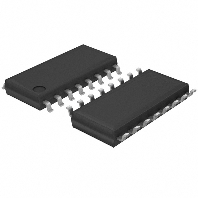
BU4015B / BU4015BF
The BU4015B and BU4015BF are 4-stage static shift registers, each consisting of two circuits.
The D flip-flops for each stage share a common reset input, enabling external asynchronous reset at any point.
Also, the flip-flops at each stage are triggered by the rising edge of the clock input.
“H” level reset input resets the contents of all stages to “L”, regardless of the clock and data input, and sets data outputs Q0 to Q3 to “L”.
•1)Features
Low power dissipation.
2) Wide range of operating power supply voltages.
3) High input impedance.
•Block diagram
4) High fan-out.
5) Direct drive of 2 L-TTL inputs and 1 LS-TTL input.
•Logic circuit diagram
Q1
Q0
CLOCK
B
1
16
VDD
Q3B
2
15
DB
Q2B
3
14
RESET
B
Q1A
4
13
Q0B
Q0A
5
12
Q1B
11
Q2B
D
CL
R
D
Q3 Q2 Q1 Q0
CLOCK
D
Q
CLR Q
D
Q
CLR Q
Q2
D
Q
CLR Q
Q3
D
Q
CLR Q
RESET
Q 0 Q1 Q2 Q3
RESET
A
6
DA
7
10
Q3A
VSS
8
9
CLOCK
A
CL
R
D
•Truth table
CLOCK
X
D
RESET
Q0
Q1
Q2
Q3
L
H
L
L
Q0
Q1
Q2
L
H
Q0
Q1
Q2
X
L
X
H
No Change
L
L
L
L
X : Irrelevant
1
�Standard ICs
BU4015B / BU4015BF
•Absolute maximum ratings (V
SS
= 0V, Ta = 25°C)
Parameter
Symbol
Limits
Power supply voltage
VDD
– 0.3 ~ + 18
V
Power dissipation
Pd
1000 (DIP), 500 (SOP)
mW
Operating temperature
Topr
– 40 ~ + 85
°C
Storage temperature
Tstg
– 55 ~ + 150
°C
– 0.3 ~ VDD + 0.3
V
Input voltage
VIN
characteristics
•DCElectrical
characteristics (unless otherwise noted, Ta = 25°C, V
Parameter
Input high level voltage
Input low level voltage
= 0V)
Symbol
Min.
3.5
—
—
VIH
7.0
—
—
11.0
—
—
15
—
—
1.5
5
—
—
3.0
—
—
4.0
VIL
Typ.
SS
Max.
Unit
Conditions
VDD (V)
5
V
V
10
—
10
—
15
Input high level current
IIH
—
—
0.3
µA
15
VIH = 15V
Input low level current
IIL
—
—
– 0.3
µA
15
VIL = 0V
4.95
—
—
Output high level voltage
Output low level voltage
VOH
VOL
Output high level current
Output low level current
Static current dissipation
IOH
IOL
IDD
5
V
9.95
—
—
14.95
—
—
—
—
0.05
—
—
0.05
—
—
0.05
15
—
—
5
– 0.16
2
Unit
– 0.4
—
—
– 1.2
—
—
0.44
—
—
1.1
—
—
3.0
—
—
—
—
20
—
—
40
—
—
80
10
IO = 0mA
15
5
V
mA
mA
10
IO = 0mA
VOH = 4.6V
10
VOH = 9.5V
15
VOH = 13.5V
5
VOL = 0.4V
10
VOL = 0.5V
15
VOL = 1.5V
5
µA
10
15
VI = VDD or GND
�Standard ICs
BU4015B / BU4015BF
Switching characteristics (unless otherwise noted, Ta = 25°C, VSS = 0V, CL = 50pF)
Parameter
Output rise time
Output fall time
Propagation delay time,
CLOCK, D→Q
Propagation delay time,
RESET to Q
Setup time
Minimum clock
pulse width
Minimum reset
pulse width
Maximum clock
frequency
Maximum clock rise
time and fall time
Input capacitance
Symbol
tTLH
tTHL
tPLH
tPHL
tPLH
tPHL
tsu
tWH (CLK)
tWH (R)
f (CLK) Max.
tr (CLK)
tf (CLK)
CIN
Min.
Typ.
Max.
Unit
—
180
—
—
90
—
—
65
—
15
—
100
—
5
VDD (V)
Conditions
5
ns
ns
10
—
50
—
—
40
—
10
—
310
—
—
125
—
—
90
—
15
—
460
—
5
—
—
15
5
ns
ns
10
—
180
—
—
120
—
15
—
100
—
5
ns
10
—
50
—
—
40
—
10
—
185
—
—
85
—
—
55
—
15
—
200
—
5
—
80
—
—
60
—
—
20
—
—
6.0
—
—
7.5
—
15
—
100
—
5
—
40
—
—
15
—
—
5
—
—
—
—
15
5
ns
ns
10
10
—
—
15
5
MHz
µs
10
10
—
—
15
pF
—
—
3
�Standard ICs
BU4015B / BU4015BF
•Measurement circuits
VDD
20ns
20ns
tSU
tSU
D
D
P. G. 2
Q0
20ns
Q1
tWH
Q2
CL
R
P. G. 1
20ns
CLOCK
tWH
tPLH
tPHL
90%
Q0
Q3
CL
VSS
CL
CL
tTLH
CL
tPHL
50%
10%
50%
tTHL
20ns
RESET
10%
GND
20ns
90%
50%
10%
tWH (R)
Fig.1 Switching characteristics measurement circuit
Fig.2 Switching time measurement waveform
•Electrical characterisistic curve
POWER DISSIPATION : Pd (mW)
1200
DIP16
1000
800
600
SOP16
400
200
0
0
25
50
75
100
125
150
AMBIENT TEMPERATURE : Ta (°C)
Fig.3 Power dissipation vs.
ambient temperature
•External dimensions (Units: mm)
BU4015B
BU4015BF
10.0 ± 0.2
19.4 ± 0.3
8
0.51Min.
6.2 ± 0.3
0.11
0.3 ± 0.1
0.5 ± 0.1
1.5 ± 0.1
3.2 ± 0.2 4.25 ± 0.3
7.62
2.54
9
1
8
1.27
0.4 ± 0.1
0.15 ± 0.1
1
16
4.4 ± 0.2
9
6.5 ± 0.3
16
0.3Min.
0° ~ 15°
0.15
DIP16
4
SOP16
�Appendix
Notes
No technical content pages of this document may be reproduced in any form or transmitted by any
means without prior permission of ROHM CO.,LTD.
The contents described herein are subject to change without notice. The specifications for the
product described in this document are for reference only. Upon actual use, therefore, please request
that specifications to be separately delivered.
Application circuit diagrams and circuit constants contained herein are shown as examples of standard
use and operation. Please pay careful attention to the peripheral conditions when designing circuits
and deciding upon circuit constants in the set.
Any data, including, but not limited to application circuit diagrams information, described herein
are intended only as illustrations of such devices and not as the specifications for such devices. ROHM
CO.,LTD. disclaims any warranty that any use of such devices shall be free from infringement of any
third party's intellectual property rights or other proprietary rights, and further, assumes no liability of
whatsoever nature in the event of any such infringement, or arising from or connected with or related
to the use of such devices.
Upon the sale of any such devices, other than for buyer's right to use such devices itself, resell or
otherwise dispose of the same, no express or implied right or license to practice or commercially
exploit any intellectual property rights or other proprietary rights owned or controlled by
ROHM CO., LTD. is granted to any such buyer.
Products listed in this document use silicon as a basic material.
Products listed in this document are no antiradiation design.
The products listed in this document are designed to be used with ordinary electronic equipment or devices
(such as audio visual equipment, office-automation equipment, communications devices, electrical
appliances and electronic toys).
Should you intend to use these products with equipment or devices which require an extremely high level of
reliability and the malfunction of with would directly endanger human life (such as medical instruments,
transportation equipment, aerospace machinery, nuclear-reactor controllers, fuel controllers and other
safety devices), please be sure to consult with our sales representative in advance.
About Export Control Order in Japan
Products described herein are the objects of controlled goods in Annex 1 (Item 16) of Export Trade Control
Order in Japan.
In case of export from Japan, please confirm if it applies to "objective" criteria or an "informed" (by MITI clause)
on the basis of "catch all controls for Non-Proliferation of Weapons of Mass Destruction.
Appendix1-Rev1.0
�
很抱歉,暂时无法提供与“BU4015BF-E2”相匹配的价格&库存,您可以联系我们找货
免费人工找货