Datasheet
Omnipolar Detection Hall IC
(Dual Outputs for both S and N Pole Polarity Detection)
BU52075GWZ
General Description
Key Specifications
The BU52075GWZ is omnipolar Hall IC incorporating a
polarity determination circuit that enables separate
operation (output) of both the South and North poles.
The polarity judgment is based on the output processing
configuration.
This Hall IC product can be in tablets, smart phones, and
other applications in order to detect open and close of
the cover.
And this Hall IC product can be in digital video cameras
and other applications involving display panels in order
to detect the front/back location or determine the
rotational direction of the panel.
VDD Voltage Range:
Operate Point:
Hysteresis:
Period:
Supply Current (AVG):
Output Type:
Operating Temperature Range:
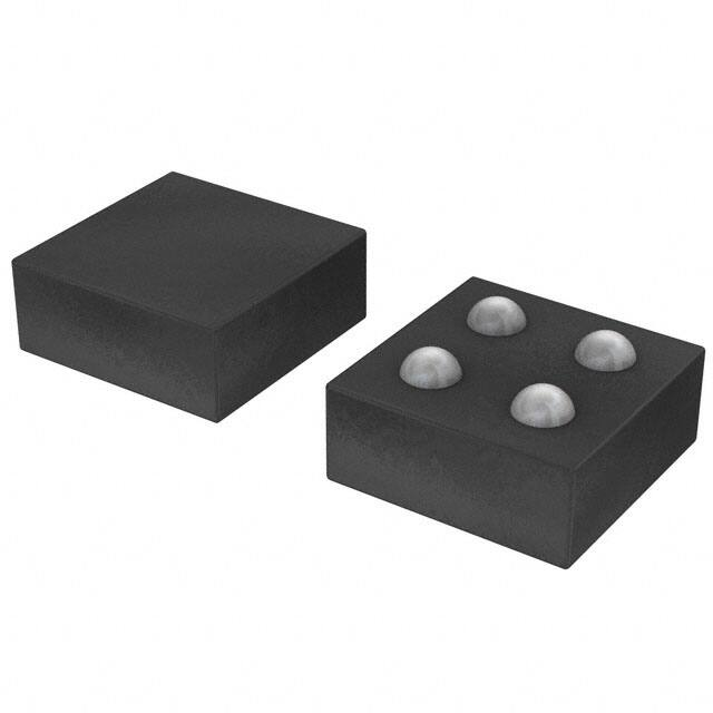
Package
1.65V to 3.6V
±9.5mT(Typ)
0.9mT(Typ)
50ms(Typ)
5.0µA (Typ)
CMOS
-40°C to +85°C
W(Typ) x D(Typ) x H(Max)
0.80mm x 0.80mm x 0.40mm
UCSP35L1
Features
Omnipolar Detection (Polarity Detection for both S
and N Poles with Separate, Dual Outputs)
Micro Power Operation (Small Current Using
Intermittent Operation Method)
Ultra-compact CSP4 Package (UCSP35L1)
Polarity Judgment and Separate Output on both
Poles
(OUT1=S-pole Output; OUT2=N-pole Output)
High ESD Resistance 8kV(HBM)
Applications
Tablets, Smart Phones, Notebook Computers,
Digital Video Cameras, Digital Still Cameras, etc.
Typical Application Circuit, Block Diagram, Pin Configurations and Pin Descriptions
VDD
0.1µF
B1
Adjust the bypass capacitor value
as necessary, according to voltage
noise conditions, etc.
LATCH
TIMING
LOGIC
The CMOS output terminals
enable direct connection to
the PC, with no external
pull-up resistor required.
GND
VDD
LATCH
×
B2 OUT1
SAMPLE
& HOLD
ELEMENT
DYNAMIC
OFFSET
CANCELLATION
HALL
A2 OUT2
A1
GND
Pin No.
Pin Name
Function
A1
GND
Ground
A2
OUT2
Output (React to the north pole)
B1
VDD
B2
OUT1
(TOP VIEW)
A1
(BOTTOM VIEW)
A2
A2
A1
B2
B1
Power supply
B1
B2
Output (React to the south pole)
〇Product structure : Silicon monolithic integrated circuit
.www.rohm.com
© 2014 ROHM Co., Ltd. All rights reserved.
TSZ22111 • 14 • 001
〇This product has no designed protection against radioactive rays
1/16
TSZ02201-0M2M0F414030-1-2
17.Oct.2014 Rev.001
�BU52075GWZ
Contents
General Description ....................................................................................................................................................1
Features .......................................................................................................................................................................1
Applications ................................................................................................................................................................1
Key Specifications ......................................................................................................................................................1
Package
W(Typ) x D(Typ) x H(Max) ........................................................................................................................1
Typical Application Circuit, Block Diagram, Pin Configurations and Pin Descriptions ......................................1
Absolute Maximum Ratings (Ta = 25°C) ...................................................................................................................3
Recommended Operating Conditions (Ta= -40°C to +85°C) ...................................................................................3
Magnetic, Electrical Characteristics (Unless otherwise specified VDD=1.80V Ta=25°C)......................................3
Measurement Circuit ..................................................................................................................................................4
Typical Performance Curves .....................................................................................................................................5
Figure 6. Operate Point, Release Point vs Ambient Temperature ......................................................................5
Figure 7. Operate Point, Release Point vs Supply Voltage .................................................................................5
Figure 8. Period vs Ambient Temperature ............................................................................................................5
Figure 9. Period vs Supply Voltage .......................................................................................................................5
Figure 10. Supply Current vs Ambient Temperature ...........................................................................................6
Figure 11. Supply Current vs Supply Voltage.......................................................................................................6
Description of Operations ..........................................................................................................................................7
Intermittent Operation at Power ON .......................................................................................................................10
Magnet Selection ......................................................................................................................................................10
Slide-by Position Sensing ........................................................................................................................................ 11
Position of the Hall Element (Reference) ............................................................................................................... 11
Footprint Dimensions (Optimize footprint dimensions to the board design and soldering condition) .......... 11
I/O Equivalence Circuit ............................................................................................................................................. 11
Operational Notes .....................................................................................................................................................12
Ordering Information ................................................................................................................................................14
Marking Diagrams .....................................................................................................................................................14
Physical Dimension, Tape and Reel Information ...................................................................................................15
Revision History .......................................................................................................................................................16
www.rohm.com
© 2014 ROHM Co., Ltd. All rights reserved.
TSZ22111 • 15 • 001
2/16
TSZ02201-0M2M0F414030-1-2
17.Oct.2014 Rev.001
�BU52075GWZ
Absolute Maximum Ratings (Ta = 25°C)
Parameter
Symbol
Rating
Unit
(Note 1)
Power Supply Voltage
VDD
-0.1 to +4.5
V
Output Current
IOUT
±0.5
Power Dissipation
Pd
0.10
(Note 2)
W
Operating Temperature Range
Topr
-40 to +85
°C
Storage Temperature Range
Tstg
-40 to +125
°C
mA
(Note 1) Not to exceed Pd
(Note 2) Mounted on 24mm x 20mm x 1.6mm glass epoxy board. Reduce 1.00mW per 1°C above 25°C
Caution: Operating the IC over the absolute maximum ratings may damage the IC. The damage can either be a short circuit between pins or an open circuit
between pins and the internal circuitry. Therefore, it is important to consider circuit protection measures, such as adding a fuse, in case the IC is operated over
the absolute maximum ratings.
Recommended Operating Conditions (Ta= -40°C to +85°C)
Parameter
Power Supply Voltage
Symbol
Min
Typ
Max
Unit
VDD
1.65
1.80
3.60
V
Magnetic, Electrical Characteristics (Unless otherwise specified VDD=1.80V Ta=25°C)
Parameter
Symbol
Min
Typ
Max
BopS
-
9.5
11.6
BopN
-11.6
-9.5
-
BrpS
6.5
8.6
-
BrpN
-
-8.6
-6.5
BhysS
-
0.9
-
BhysN
-
0.9
-
Tp
-
50
100
ms
Output High Voltage
VOH
VDD
-0.2
-
-
V
Output Low Voltage
VOL
-
-
0.2
V
IDD(AVG)
-
5
8
µA
Average
IDD(EN)
-
2.8
-
mA
During startup time value
IDD(DIS)
-
1.8
-
µA
During standby time value
Operate Point
mT
Release Point
mT
Hysteresis
Period
Supply Current
Supply Current During Startup
Time
Supply Current During Standby
Time
Unit
Conditions
Output: OUT1
(React to the south pole)
Output: OUT2
(React to the north pole)
Output: OUT1
(React to the south pole)
Output: OUT2
(React to the north pole)
mT
(Note 3)
BrpN
很抱歉,暂时无法提供与“BU52075GWZ-E2”相匹配的价格&库存,您可以联系我们找货
免费人工找货- 国内价格 香港价格
- 1+2.837831+0.34300
- 10+2.3270210+0.28126
- 50+1.3297350+0.16072
- 100+1.26486100+0.15288
- 500+1.02973500+0.12446
- 1000+0.997301000+0.12054
- 2000+0.924332000+0.11172
- 4000+0.916224000+0.11074
- 国内价格 香港价格
- 1+2.837831+0.34300
- 10+2.3270210+0.28126
- 50+1.3297350+0.16072
- 100+1.26486100+0.15288
- 500+1.02973500+0.12446
- 1000+0.997301000+0.12054
- 2000+0.924332000+0.11172
- 4000+0.916224000+0.11074


 工商网监
湘ICP备2023018690号
工商网监
湘ICP备2023018690号
