Communication ICs
Panel interface
BU8310AK / BU8311KS / BU8313K
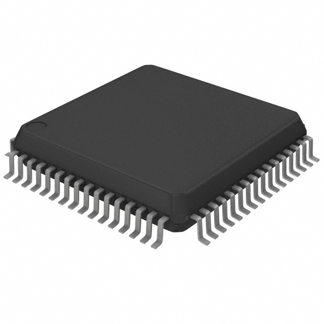
The BU8310AK, BU8311KS, and BU8313K are large-scale integrated circuits for telephones, which enable a serial input / output interface between the key input required for telephone panel boards and LED control functions. They reduce the number of wiring harnesses needed between the main board in the telephone and the panel board, and take some of the processing load off the main CPU.
FApplications Telephones and cordless telephones
FFeatures 1) Keypad matrix interface 1 Key input is output as 16-bit serial data. 2 Internal chattering prevention circuit built into the key input circuit.
2) LED interface 1 LED control commands input as 16-bit serial data. 2 Bits with a pattern generator and pattern register can be assigned three independent flashing patterns in addition to being lighted or off. 3 Power consumption can be reduced using RST pin input. 4 LED on and off control can be initiated using ENA pin input or by commands setting all LEDs valid or invalid.
277
�Communication ICs
FBlock diagram
BU8310AK / BU8311KS / BU8313K
278
�Communication ICs
BU8310AK / BU8311KS / BU8313K
279
�Communication ICs
FAbsolute maximum ratings (Ta = 25_C)
BU8310AK / BU8311KS / BU8313K
FRecommended operating conditions
FPin descriptions
280
�Communication ICs
BU8310AK / BU8311KS / BU8313K
FInput / output circuits
281
�Communication ICs
BU8310AK / BU8311KS / BU8313K
FElectrical characteristics DC characteristics (unless otherwise noted,Ta = 25_C, VDD = 3 X 5V)
AC characteristics (unless otherwise noted, Ta = 25_C, VDD = 3 X 5V)
282
�Communication ICs
Serial data output timing
BU8310AK / BU8311KS / BU8313K
Serial data input timing
283
�Communication ICs
BU8310AK / BU8311KS / BU8313K
FData formats (Serial data is input and output with the MSB coming first.) (1) Reading key data
(2) Data register write command
(3) Pattern register write command
(4) All LEDs valid command
(5) All LEDs invalid command
284
�Communication ICs
(6) Register reset command
BU8310AK / BU8311KS / BU8313K
FEntering data settings (1) Setting operands
(2) Setting the blink cycle
FDriver internal equivalent circuit (for 1 bit)
285
�Communication ICs
FRecommended method for inputting / outputting data (1) Serial output of key data
BU8310AK / BU8311KS / BU8313K
(2) Serial input of LED control commands
286
�Communication ICs
FOperation notes (1) Serial output of key data when several keys are pressed at the same is as shown below.
BU8310AK / BU8311KS / BU8313K
(3) When the power supply is turned on, the internal registers should be reset using either RST pin input or the register reset command. (4) If the RST pin is set to LOW or the register reset command is executed while data is being output, the SDO output logic is not reset. (5) If the D, P, and Q registers are rewritten, all eight bits should be written, and not just the pertinent bits.
The key data when 32 and 43 are pressed at the same time will be the same as the key data when 33 and 42 are pressed at the same time. (2) Pressing different keys
When a different key is pressed from the one already pressed, KD is turned temporarily to provide notification of the change. (6) Operation states in response to RST, KSCN and ENA pin input
287
�Communication ICs
FExternal dimensions (Units: mm)
BU8310AK / BU8311KS / BU8313K
288
�
很抱歉,暂时无法提供与“BU8310AK”相匹配的价格&库存,您可以联系我们找货
免费人工找货