Datasheet
Single-chip Type with Built-in FET Switching Regulator Series
Step-down Switching regulators
with Built-in Power MOSFET
BU9002xNUX Series
●General Description
The BU9002xNUX are a high efficiency 1MHz
synchronous step-down switching regulator with low
current PFM mode.
It provides up to 1.5A load current and an input voltage
range from 4.5V to 5.5V, optimized for various
applications with input voltage range up to 5V.
BU9002xNUX has a mode control pin that allows the
user to select Forced PWM (Pulse Width Modulation)
mode or PFM (Pulse Frequency Modulation) and PWM
auto change mode utilized power save operation at light
load current.
●Applications
POL, 1Cell Li-ion battery for portable applications ,
USB accessories
W(Typ.) x D(Typ.) x H(Max.)
2.00mm x 3.00mm x 0.60mm
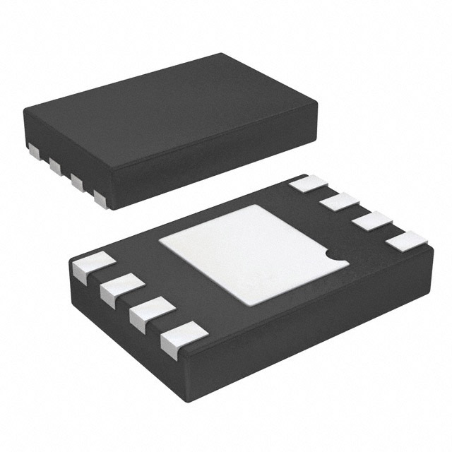
●Package(s)
VSON008X2030
●Features
■ Fast transient response
■ Automatic PFM/PWM operation.
■ Forced PWM operation
■ Internal Soft Start
■ Under voltage lockout
■ Over current protection
■ Thermal shutdown
VSON008X2030
●Typical Application Circuit(s)
●Lineup
Part No.
Output
voltage
BU90023NUX
1.230V
BU90028NUX
1.175V
Figure 1. Typical Application Circuit(s)
●Pin Description(s)
●Pin Configuration(s)
Pin No.
(TOP VIEW)
LX
Symbol
Function
1
LX
Inductor connection pin
2
MODE
Forced PWM mode pin
3
PVIN
Power supply input pin
4
VIN
Power supply input pin
AGND
5
EN
Enable pin
EN
6
AGND
GND pin
7
PGND
GND pin
8
FB
FB
MODE
PGND
PVIN
VIN
Figure 2. Pin Configuration(s)
Feedback voltage input pin
○Product structure : Silicon monolithic integrated circuit ○This product is not designed protection against radioactive rays
www.rohm.com
TSZ02201-0F2F0AG00020-1-2
© 2012 ROHM Co., Ltd. All rights reserved.
1/11
21.JUN.2012 Rev.001
TSZ22111・14・001
�Datasheet
BU9002xNUX Series
●Block Diagram(s)
MODE
AVIN
TSD
UVLO
PWM/PFM
control
PVIN
C
Current
sense
FB
+
ERROR AMP
Switching
Control Logic
and
Gate Driver
L
LX
OUTPUT
C
VREF
EN
SHUTDOWN
Frequency
control
PGND
ON/OFF
AGND
Figure 3. Block Diagram(s)
●Description of Block(s)
The BU9002xNUX are a synchronous step-down DC/DC converter that achieves fast transient response from light load to heavy
load by hysteretic PWM control system and current constant PFM control system.
○PWM control
BU9002xNUX operates by hysteretic PWM control. This scheme ensures fast switching, high efficiency, and fast transient
response.
When the output voltage is below the VREF voltage, the error comparator output is low to high and turning on P-channel
MOSFET until above the VREF voltage and minimum on time.
○PFM control
At light load the regulator and MODE=low, the regulator operates with reduced switching frequency and improves the efficiency.
During PFM operation, the output voltage slightly higher than typical output voltage.
Figure 4. Operation of PFM mode and PWM mode
www.rohm.com
© 2012 ROHM Co., Ltd. All rights reserved.
TSZ22111・15・001
2/11
TSZ02201-0F2F0AG00020-1-2
21.JUN.2012 Rev.001
�Datasheet
BU9002xNUX Series
●Description of operations
1) Shutdown
If the EN input pin set to low (2.05V(typ.)
5) FORCED PWM MODE
Setting MODE pin high (>1.4V) places the regulator in forced PWM. This control provides noise reduction and output stability.
Do not leave the MODE pin floating.
6) TSD
The BU9002xNUX has a thermal shutdown feature to protect the device if the junction temperature exceeds 150℃.In thermal
shutdown, the DRIVER is disabled.
This circuit is only to cut off the IC from thermal runaway, and has not been design to protect or guarantee the IC. Therefore, the
user should not plan to activate this circuit with continued operation in mind.
●Absolute Maximum Ratings (Ta=25℃)
Parameter
Symbol
Rating
Unit
VIN
7
V
VEN, VFB, VLX,
VMODE
7
V
Pd
0.515
W
Operating temperature range
Topr
-40 to +85
℃
Storage temperature range
Tstg
-55 to +125
℃
Tjmax
+125
℃
Maximum input power supply voltage
Maximum voltage at EN, FB, LX, MODE
Power dissipation
Junction temperature
(*1) When mounted on the specified PCB (55mm x 63mm), Deducted by 3.9m W/c when used over Ta=25c
●Recommended Operating Rating(s)
Parameter
Symbol
Input voltage
VIN
www.rohm.com
© 2012 ROHM Co., Ltd. All rights reserved.
TSZ22111・15・001
Rating
Min.
Typ.
Max.
2.3
-
5.5
3/11
Unit
Series
V
TSZ02201-0F2F0AG00020-1-2
21.JUN.2012 Rev.001
�Datasheet
BU9002xNUX Series
●Electrical Characteristic(s) (unless otherwise specified VIN=5.0V, Ta=25℃)
Item
Min.
Rating
Typ.
Max.
1.206
1.230
1.254
1.152
1.175
1.199
Tss
120
240
480
usec
fosc
0.8
1.0
2.0
MHz
RonP
RonN
-
250
220
400
350
mOhm
mOhm
Symbol
Unit
Condition
【Switching regulator】
Output voltage accuracy
VOUTA
V
BU90023NUX MODE:H(PWM)
BU90028NUX MODE:H(PWM)
【Soft start】
Soft start time
【Frequency control】
Switching frequency
【Driver】
PchFET on resistance
NchFET on resistance
【Control】
VIN=5.0V
VIN=5.0V
EN pin control
voltage
Operation
VENH
1.4
-
VIN
V
Non Operation
VENL
0
-
0.4
V
MODE pin
control voltage
Operation
VMODEH
1.4
-
VIN
V
Forced PWM
Non Operation
VMODEL
0
-
0.4
V
Automatic PFM/PWM
Uvth
Uvhy
1.95
50
2.05
100
2.15
150
V
mV
Current limit threshold
ILIMIT
2.2
2.5
2.8
A
【Output discharge】
Output discharge resistance
【Circuit current】
DRES
55
110
220
Ohm
Operating quiescent current
IINS
53
75
uA
Shutdown current
SHD
0
1
uA
【UVLO】
Protect threshold voltage
Hysteresis
【Current limit】
www.rohm.com
© 2012 ROHM Co., Ltd. All rights reserved.
TSZ22111・15・001
-
4/11
PMOS current detect,
Open loop
EN=0V
EN:H, MODE:L,
VOUT=3.6V forced
Not switching
EN=0V
TSZ02201-0F2F0AG00020-1-2
21.JUN.2012 Rev.001
�Datasheet
BU9002xNUX Series
●Electrical characteristic curves (Reference data)
BU90023NUX (1.23V OUTPUT)
)
EN
2V/div
EN
2V/div
VOUT
1V/div
VOUT
1V/div
IL
500mA/div
Figure 5. Start up
Figure 6. Shut down
Vout
50mV/div
ac coupled
Vout
50mV/div
ac coupled
IOUT
500mA/div
IOUT
500mA/div
Figure 7. Load transient response 400mA to 800mA
tr=tf=100ns, MODE : Low
www.rohm.com
© 2012 ROHM Co., Ltd. All rights reserved.
TSZ22111・15・001
5/11
Figure 8. Load transient response 600mA to 1200mA
tr=tf=100ns, MODE : Low
TSZ02201-0F2F0AG00020-1-2
21.JUN.2012 Rev.001
�Datasheet
BU9002xNUX Series
●Electrical characteristic curves (Reference data)
BU90023NUX (1.23V OUTPUT) continued
Vout
20mV/div
ac coupled
LX
2V/div
IL
500mA/div
Figure 9. PWM mode
Operation Iout=50mA
Figure 10. Efficiency vs Load current
VIN=5V PWM/PFM Auto mode
VIN=5.5
VIN=5.0
VIN=4.0
Figure 11. Load regulation
PWM mode
www.rohm.com
© 2012 ROHM Co., Ltd. All rights reserved.
TSZ22111・15・001
6/11
TSZ02201-0F2F0AG00020-1-2
21.JUN.2012 Rev.001
�Datasheet
BU9002xNUX Series
●Electrical characteristic curves (Reference data)
BU90028NUX (1.175V OUTPUT)
EN
2V/div
EN
2V/div
VOUT
1V/div
VOUT
1V/div
IL
500mA/div
Figure 12. Start up
Figure 13. Shut down
Vout
50mV/div
ac coupled
Vout
50mV/div
ac coupled
IOUT
500mA/div
IOUT
500mA/div
Figure 14. Load transient response 400mA to 800mA
tr=tf=100ns, MODE : Low
www.rohm.com
© 2012 ROHM Co., Ltd. All rights reserved.
TSZ22111・15・001
7/11
Figure 15. Load transient response 600mA to 1200mA
tr=tf=100ns, MODE : Low
TSZ02201-0F2F0AG00020-1-2
21.JUN.2012 Rev.001
�Datasheet
BU9002xNUX Series
●特性データ(参考データ)
BU90028NUX(
(1.175V 出力)
出力)continued
Vout
20mV/div
ac coupled
LX
2V/div
IL
500mA/div
Figure 16. PWM mode
Operation Iout=50mA
Figure 17. Efficiency vs Load current
VIN=5V PWM/PFM Auto mode
VIN=5.5
VIN=5.0
VIN=4.0
Figure 18. Load regulation
PWM mode
www.rohm.com
© 2012 ROHM Co., Ltd. All rights reserved.
TSZ22111・15・001
8/11
TSZ02201-0F2F0AG00020-1-2
21.JUN.2012 Rev.001
�Datasheet
BU9002xNUX Series
●PC Board layout
The suggested PCB layout for the BU9002xNUX are shown in Figure. The following guidelines should be used to ensure a
proper layout.
1) The input capacitor CIN should be connect as closely possible to VIN pin and GND pin.
2) From the output voltage to the FB pin line should be as separate as possible.
3) COUT and L should be connected as closely as possible. The connection of L to the LX pin should be as short as possible.
Figure 19. PCB layout
●External parts selection
Inductor selection
The inductance significantly depends on output ripple current. As shown by following equation, the ripple current decreases as
the inductor and/or switching frequency increase.
(VIN-VOUT)×VOUT
⊿IL=
L×VIN×f
f: switching frequency
L: inductance
⊿IL: inductor current ripple
As a minimum requirement, the DC current rating of the inductor should be equal to the maximum load current plus half of the
inductor current ripple as shown by the following equation.
ILPEAK= IOUTMAX +
⊿IL
2
1) Recommended inductor selection
・Iout≦1.5A
DFE252012C Type 2.2uH (TOKO)
NR4018T2R2M (TAIYO YUDEN)
・Iout≦0.6A
NR3010T2R2M (TAIYO YUDEN)
2) Recommended input capacitor(CIN) selection
C1608 Type 22uF (X5R 6.3V TDK)
3)Recommended output capacitor(COUT) selection
C1608 Type 22uF (X5R 6.3V TDK)
www.rohm.com
© 2012 ROHM Co., Ltd. All rights reserved.
TSZ22111・15・001
9/11
TSZ02201-0F2F0AG00020-1-2
21.JUN.2012 Rev.001
�Datasheet
BU9002xNUX Series
●Caution of use
1) Absolute maximum ratings
An excess in the absolute maximum rating, such as supply voltage, temperature range of operating conditions, etc.,
can break down the devices, thus making impossible to identify breaking mode, such as a short circuit or an open
circuit. If any over rated values will expect to exceed the absolute maximum ratings, consider adding circuit protection
devices, such as fuses.
2) GND voltage
The potential of GND pin must be minimum potential in all condition. As an exception, the circuit design allows voltages
up to -0.3 V to be applied to the IC pin.
3) Thermal design
Use a thermal design that allows for a sufficient margin in light of the power dissipation (Pd) in actual operating
conditions.
4) Inter-pin shorts and mounting errors
Use caution when positioning the IC for mounting on printed circuit boards. The IC may be damaged if there is any
connection error or if pins are shorted together.
5) Actions in strong electromagnetic field
Use caution when using the IC in the presence of a strong electromagnetic field as doing so may cause the IC to
malfunction.
6) Mutual impedance
Power supply and ground wiring should reflect consideration of the need to lower mutual impedance and minimize
ripple as much as possible (by making wiring as short and thick as possible or rejecting ripple by incorporating
inductance and capacitance).
7) Thermal shutdown Circuit (TSD Circuit)
This model IC has a built-in TSD circuit. This circuit is only to cut off the IC from thermal runaway, and has not been
design to protect or guarantee the IC. Therefore, the user should not plan to activate this circuit with continued
operation in mind.
8) Regarding input pin of the IC
This monolithic IC contains P+ isolation and P substrate layers between adjacent elements in order to keep them
isolated.
P-N junctions are formed at the intersection of these P layers with the N layers of other elements, creating a parasitic
diode or transistor. For example, as shown in the figures below, the relation between each potential is as follows:
When GND > Pin A and GND > Pin B, the P-N junction operates as a parasitic diode.
When GND > Pin B, the P-N junction operates as a parasitic transistor.
Parasitic diodes can occur inevitable in the structure of the IC. The operation of parasitic diodes can result in mutual
interference among circuits, operational faults, or physical damage. Accordingly, methods by which parasitic diodes
operate, such as applying a voltage that is lower than the GND (P substrate) voltage to an input pin, should not be
used.
Status of this document
The Japanese version of this document is formal specification. A customer may use this translation version only for a reference
to help reading the formal version.
If there are any differences in translation version of this document formal version takes priority
www.rohm.com
© 2012 ROHM Co., Ltd. All rights reserved.
TSZ22111・15・001
10/11
TSZ02201-0F2F0AG00020-1-2
21.JUN.2012 Rev.001
�Datasheet
BU9002xNUX Series
●Ordering Information
B
U
9
0
0
2
x
N
U
X
TR
Package
NUX: VSON008X2030
Part Number
Packaging and forming specification
TR: Embossed tape and reel
(VSON008X2030)
●Physical Dimension Tape and Reel Information
VSON008X2030
2.0±0.1
3.0±0.1
Tape
Quantity
0.6MAX
1PIN MARK
Direction
of feed
0.3±0.1
C0.25
0.25
1.5±0.1
4000pcs
TR
The direction is the 1pin of product is at the upper right when you hold
)
(0.12)
( reel on the left hand and you pull out the tape on the right hand
0.5
1
4
8
5
1.4±0.1
0.08 S
+0.03
0.02 −0.02
S
Embossed carrier tape
Direction of feed
1pin
+0.05
0.25 −0.04
(Unit : mm)
Reel
∗ Order quantity needs to be multiple of the minimum quantity.
●Marking Diagram(s)(TOP VIEW)
VSON008X2030 (TOP VIEW)
Part Number Marking
LOT Number
Part No.
BU90023NUX
BU90028NUX
Part Number
Marking
U90
023
U90
028
1PIN MARK
www.rohm.com
© 2012 ROHM Co., Ltd. All rights reserved.
TSZ22111・15・001
11/11
TSZ02201-0F2F0AG00020-1-2
21.JUN.2012 Rev.001
�Datasheet
Notice
Precaution on using ROHM Products
1.
Our Products are designed and manufactured for application in ordinary electronic equipments (such as AV equipment,
OA equipment, telecommunication equipment, home electronic appliances, amusement equipment, etc.). If you
(Note 1)
, transport
intend to use our Products in devices requiring extremely high reliability (such as medical equipment
equipment, traffic equipment, aircraft/spacecraft, nuclear power controllers, fuel controllers, car equipment including car
accessories, safety devices, etc.) and whose malfunction or failure may cause loss of human life, bodily injury or
serious damage to property (“Specific Applications”), please consult with the ROHM sales representative in advance.
Unless otherwise agreed in writing by ROHM in advance, ROHM shall not be in any way responsible or liable for any
damages, expenses or losses incurred by you or third parties arising from the use of any ROHM’s Products for Specific
Applications.
(Note1) Medical Equipment Classification of the Specific Applications
JAPAN
USA
EU
CHINA
CLASSⅢ
CLASSⅡb
CLASSⅢ
CLASSⅢ
CLASSⅣ
CLASSⅢ
2.
ROHM designs and manufactures its Products subject to strict quality control system. However, semiconductor
products can fail or malfunction at a certain rate. Please be sure to implement, at your own responsibilities, adequate
safety measures including but not limited to fail-safe design against the physical injury, damage to any property, which
a failure or malfunction of our Products may cause. The following are examples of safety measures:
[a] Installation of protection circuits or other protective devices to improve system safety
[b] Installation of redundant circuits to reduce the impact of single or multiple circuit failure
3.
Our Products are designed and manufactured for use under standard conditions and not under any special or
extraordinary environments or conditions, as exemplified below. Accordingly, ROHM shall not be in any way
responsible or liable for any damages, expenses or losses arising from the use of any ROHM’s Products under any
special or extraordinary environments or conditions. If you intend to use our Products under any special or
extraordinary environments or conditions (as exemplified below), your independent verification and confirmation of
product performance, reliability, etc, prior to use, must be necessary:
[a] Use of our Products in any types of liquid, including water, oils, chemicals, and organic solvents
[b] Use of our Products outdoors or in places where the Products are exposed to direct sunlight or dust
[c] Use of our Products in places where the Products are exposed to sea wind or corrosive gases, including Cl2,
H2S, NH3, SO2, and NO2
[d] Use of our Products in places where the Products are exposed to static electricity or electromagnetic waves
[e] Use of our Products in proximity to heat-producing components, plastic cords, or other flammable items
[f] Sealing or coating our Products with resin or other coating materials
[g] Use of our Products without cleaning residue of flux (even if you use no-clean type fluxes, cleaning residue of
flux is recommended); or Washing our Products by using water or water-soluble cleaning agents for cleaning
residue after soldering
[h] Use of the Products in places subject to dew condensation
4.
The Products are not subject to radiation-proof design.
5.
Please verify and confirm characteristics of the final or mounted products in using the Products.
6.
In particular, if a transient load (a large amount of load applied in a short period of time, such as pulse. is applied,
confirmation of performance characteristics after on-board mounting is strongly recommended. Avoid applying power
exceeding normal rated power; exceeding the power rating under steady-state loading condition may negatively affect
product performance and reliability.
7.
De-rate Power Dissipation (Pd) depending on Ambient temperature (Ta). When used in sealed area, confirm the actual
ambient temperature.
8.
Confirm that operation temperature is within the specified range described in the product specification.
9.
ROHM shall not be in any way responsible or liable for failure induced under deviant condition from what is defined in
this document.
Precaution for Mounting / Circuit board design
1.
When a highly active halogenous (chlorine, bromine, etc.) flux is used, the residue of flux may negatively affect product
performance and reliability.
2.
In principle, the reflow soldering method must be used; if flow soldering method is preferred, please consult with the
ROHM representative in advance.
For details, please refer to ROHM Mounting specification
Notice - GE
© 2014 ROHM Co., Ltd. All rights reserved.
Rev.002
�Datasheet
Precautions Regarding Application Examples and External Circuits
1.
If change is made to the constant of an external circuit, please allow a sufficient margin considering variations of the
characteristics of the Products and external components, including transient characteristics, as well as static
characteristics.
2.
You agree that application notes, reference designs, and associated data and information contained in this document
are presented only as guidance for Products use. Therefore, in case you use such information, you are solely
responsible for it and you must exercise your own independent verification and judgment in the use of such information
contained in this document. ROHM shall not be in any way responsible or liable for any damages, expenses or losses
incurred by you or third parties arising from the use of such information.
Precaution for Electrostatic
This Product is electrostatic sensitive product, which may be damaged due to electrostatic discharge. Please take proper
caution in your manufacturing process and storage so that voltage exceeding the Products maximum rating will not be
applied to Products. Please take special care under dry condition (e.g. Grounding of human body / equipment / solder iron,
isolation from charged objects, setting of Ionizer, friction prevention and temperature / humidity control).
Precaution for Storage / Transportation
1.
Product performance and soldered connections may deteriorate if the Products are stored in the places where:
[a] the Products are exposed to sea winds or corrosive gases, including Cl2, H2S, NH3, SO2, and NO2
[b] the temperature or humidity exceeds those recommended by ROHM
[c] the Products are exposed to direct sunshine or condensation
[d] the Products are exposed to high Electrostatic
2.
Even under ROHM recommended storage condition, solderability of products out of recommended storage time period
may be degraded. It is strongly recommended to confirm solderability before using Products of which storage time is
exceeding the recommended storage time period.
3.
Store / transport cartons in the correct direction, which is indicated on a carton with a symbol. Otherwise bent leads
may occur due to excessive stress applied when dropping of a carton.
4.
Use Products within the specified time after opening a humidity barrier bag. Baking is required before using Products of
which storage time is exceeding the recommended storage time period.
Precaution for Product Label
QR code printed on ROHM Products label is for ROHM’s internal use only.
Precaution for Disposition
When disposing Products please dispose them properly using an authorized industry waste company.
Precaution for Foreign Exchange and Foreign Trade act
Since our Products might fall under controlled goods prescribed by the applicable foreign exchange and foreign trade act,
please consult with ROHM representative in case of export.
Precaution Regarding Intellectual Property Rights
1.
All information and data including but not limited to application example contained in this document is for reference
only. ROHM does not warrant that foregoing information or data will not infringe any intellectual property rights or any
other rights of any third party regarding such information or data. ROHM shall not be in any way responsible or liable
for infringement of any intellectual property rights or other damages arising from use of such information or data.:
2.
No license, expressly or implied, is granted hereby under any intellectual property rights or other rights of ROHM or any
third parties with respect to the information contained in this document.
Other Precaution
1.
This document may not be reprinted or reproduced, in whole or in part, without prior written consent of ROHM.
2.
The Products may not be disassembled, converted, modified, reproduced or otherwise changed without prior written
consent of ROHM.
3.
In no event shall you use in any way whatsoever the Products and the related technical information contained in the
Products or this document for any military purposes, including but not limited to, the development of mass-destruction
weapons.
4.
The proper names of companies or products described in this document are trademarks or registered trademarks of
ROHM, its affiliated companies or third parties.
Notice - GE
© 2014 ROHM Co., Ltd. All rights reserved.
Rev.002
�Datasheet
General Precaution
1. Before you use our Pro ducts, you are requested to care fully read this document and fully understand its contents.
ROHM shall n ot be in an y way responsible or liabl e for fa ilure, malfunction or acci dent arising from the use of a ny
ROHM’s Products against warning, caution or note contained in this document.
2. All information contained in this docume nt is current as of the issuing date and subj ect to change without any prior
notice. Before purchasing or using ROHM’s Products, please confirm the la test information with a ROHM sale s
representative.
3.
The information contained in this doc ument is provi ded on an “as is” basis and ROHM does not warrant that all
information contained in this document is accurate an d/or error-free. ROHM shall not be in an y way responsible or
liable for an y damages, expenses or losses incurred b y you or third parties resulting from inaccur acy or errors of or
concerning such information.
Notice – WE
© 2014 ROHM Co., Ltd. All rights reserved.
Rev.001
�


 工商网监
湘ICP备2023018690号
工商网监
湘ICP备2023018690号
