MCH18
Ceramic capacitors
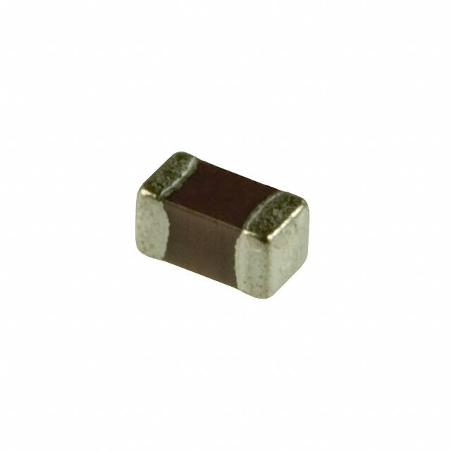
Multi-layer ceramic chip capacitors
MCH18 (1608 (0603) size, chip capacitor)
!External dimensions (Units : mm)
!Features
1) Small size (1.6 x 0.8 x 0.8 mm) makes it perfect
for lightweight portable devices.
2) Comes packed either in tape to enable automatic
mounting or in bulk cases.
3) Precise uniformity of shape and dimentions highly efficient
automatic mounting.
4) Barrier layer and end terminations to improve
solderability.
0.15Min. 0.4Min.
0.8±0.1
0.8±0.1
0.8±0.1
1.6±0.1
0.8±0.1
!Structure
External electrode ΙΙΙ (coating layer)
Internal electrode
Ceramic element
External electrode ΙΙ (barrier layer)
External electrode Ι (thick membrane layer)
!Product designation
Code Product thickness Packaging specifications
Reel
Basic ordering (pcs.)
K
0.8mm Paper tape (width 8 mm, pitch 4 mm) φ180mm (7in.)
4,000
0.8mm Paper tape (width 8 mm, pitch 4 mm) φ330mm (13in.)
L
16,000
C
15,000
0.8mm
Bulk case
−
Ree l(φ180,φ330mm) : compatible with EIAJ ET-7200A
Bulk case :compatible with EIAJ ET-7201A
Part No.
M C H
Rated voltage
Code Voltage
2
25V
3
16V
5
50V
Packaging style
1 8
2
F N
1 0 4
Z
K
Capacitance-temperature characteristics
Nominal
Capacitance tolerance
Code Code Operating temperature (ºC) Temp. coefficient or percent change capacitance Code
tolerance
±30ppm/°C
−55~+125
A CG(C0G)
C ±0.25pF (0.5 ~ 5pF)
D ±0.5pF (5.1 ~ 10pF)
R
−55~+125
±15%
CN
B
−25~+85
±10%
3-digit designation J ±5% (11pF or more)
(X7R)
(−55~+125)
(±15%)
according to IEC
K
±10%
F
−25~+85
+30%,−80%
FN
(Y5V)
(+22%,−82%)
(−30~+85)
Z
+80%, −20%
∗The design and specifications are subject to change without prior notice. Before ordering or using, please check the latest technical specification.
�MCH18
Ceramic capacitors
!Capacitance range
For thermal compensation
Part number.
Tolerance
Part number.
MCH18
Temperature A (CG) (C0G)
characteristics
Capacitance(pF)
Rated voltage
(V)
50
Tolerance
0.5
0.75
1
110
120
130
1.1
1.2
1.3
150
160
180
1.5
1.6
1.8
200
220
240
2
2.2
2.4
C ( ± 0.25pF)
270
300
330
2.7
3
3.3
360
390
430
3.6
3.9
4
470
510
560
4.3
4.7
5
620
680
750
5.1
5.6
6
820
910
1,000
6.2
6.8
7
7.5
8
8.2
MCH18
Temperature A (CG) (C0G)
characteristics
Capacitance (pF)
Rated voltage
(V)
50
J ( ± 5%)
Product thickness (mm) 0.8 ± 0.1
D ( ± 0.5pF)
9
9.1
10
11
12
13
15
16
18
20
22
24
27
30
33
36
39
43
J ( ± 5%)
47
51
56
62
68
75
82
91
100
∗The design and specifications are subject to change without prior notice. Before ordering or using, please check the latest technical specification.
�MCH18
Ceramic capacitors
High dielectric constant
Part number
Capacitance(pF)
Temperature
characteristics
Rated voltage (V)
Tolerance
MCH18
CN (R) (B) (X7R)
50
25
K (±10%)
FN (F) (Y5V)
50
25
16
Z (+80%, −20%)
220
270
330
390
470
560
680
820
1,000
1,200
1,500
1,800
2,200
2,700
3,300
3,900
4,700
5,600
6,800
8,200
10,000 (0.01µF)
12,000
15,000
18,000
22,000
27,000
33,000
39,000
47,000
56,000
68,000
82,000
100,000 (0.1µF)
120,000
150,000
180,000
220,000
270,000
330,000
390,000
470,000
560,000
680,000
1,000,000 (1µF)
1,200,000
1,500,000
1,800,000
2,200,000
Product thickness (mm) 0.8 ± 0.1
∗The design and specifications are subject to change without prior notice. Before ordering or using, please check the latest technical specification.
�MCH18
Ceramic capacitors
!Characteristics
Class 1 (For thermal compensation)
Temperature characteristics
A (CG) (C0G)
Item
Operating temperature
Test methods / conditions
(based on JIS C 5102)
−55°C ~ +125°C
Nominal capacitance (C)
Must be within the specified tolerance range.
Based on paragraph 7.8 and paragraph 9
Measured at room temperature and standard humidity.
Dissipation factor (tan δ )
100 / (400 + 20C)% or less
(Less than 30 pF)
0.1% or less (30 pF or larger)
1000pF or less Measurement frequency : 1± 0.1MHz
Measurement voltage : 1± 0.1Vrms.
Over 1000pF Measurement frequency : 1± 0.1kHz
Measurement voltage : 1± 0.1Vrms.
Insulation resistance (IR)
10,000MΩ or 500ΜΩ⋅µF , whichever is smaller
Withstanding voltage
Temperature characteristics
Terminal adherence
Appearance
Resistance
to vibration
Rate of capacitance change
Dissipation factor (tanδ)
Appearance
Rate of capacitance change
Temperature
cycling
Hightemperature
load test
No detachment or signs of detachment.
There must be no mechanical damage.
Must be within initial tolerance.
Must satisfy initial specified value.
± 2.5% or ± 0.25 pF , whichever is larger.
Must satisfy initial specified value.
Insulation resistance
10,000MΩ or 500ΜΩ⋅µF , whichever is smaller
Withstanding voltage
The insulation must not be damaged.
Appearance
There must be no mechanical damage.
Rate of capacitance change
± 2.5% ± 0.25 pF , whichever is larger.
Dissipation factor (tanδ)
Must satisfy initial specified value.
Insulation resistance
10,000MΩ or 500ΜΩ⋅µF , whichever is smaller
Rate of capacitance change
The temperature coefficients in table 12, paragraph
7.12 are calculated at 20°C and high temperature.
Based on paragraph 8.11.2
Apply 5N for 10 ± 1s
in the direction indicated
by the arrow.
Pressure (5N)
Test board
Capacitor
Chip is mounted to a board in the
manner shown on the right, subjected
to vibration (type A in paragraph 8.2),
and measured 24 ± 2 hrs. later.
Board
Based on paragraph 8.13
Soldering temperature : 235 ± 5°C
Soldering time
: 2 ± 0.5s
There must be no mechanical damage.
Dissipation factor (tanδ)
Appearance
Humidity load
test
Within 0 ± 30ppm / °C
At least 3 / 4 of the surface of the two terminals
must be covered with new solder.
Solderability
Resistance
to soldering
heat
The insulation must not be damaged.
Based on paragraph 7.6
Measurement is made after rated voltage
is applied for 60 ± 5s.
Based on paragraph 7.1
Apply 300% of the rated voltage
for 1 to 5s then measure.
There must be no mechanical damage.
± 7.5% or ± 0.75 pF , whichever is larger.
Dissipation factor (tanδ)
0.5% or less
Insulation resistance
500MΩ or 25ΜΩ⋅µF , whichever is smaller
Appearance
There must be no mechanical damage.
Rate of capacitance change
± 3.0% or ± 0.3 pF , whichever is larger.
Dissipation factor (tanδ)
0.3% or less
Insulation resistance
1,000MΩ or 50ΜΩ⋅µF , whichever is smaller
Based on paragraph 8.14
Soldering temperature : 260 ± 5°C
Soldering time
: 5 ± 0.5s
Preheating
: 150 ± 10°C for
1 to 2 min.
Based on paragraph 9.3
Number of cycles : 5
Capacitance measured after 24 ± 2 hrs.
Based on paragraph 9.9
Test temperature : 40 ± 2°C
Relative humidity : 90% to 95%
Applied voltage : rated voltage
Test time
: 500 to 524 hrs.
Capacitance measured after 24 ± 2 hrs.
Based on paragraph 9.10
Test temperature : Max. operating temp.
Applied voltage : rated voltage × 200%
Test time
: 1,000 to 1,048 hrs.
Capacitance measured after 24 ± 2 hrs.
∗The design and specifications are subject to change without prior notice. Before ordering or using, please check the latest technical specification.
�MCH18
Ceramic capacitors
Class 2 (High dielectric constant)
Temperature characteristics
CN (R) (B) (X7R)
FN (F) (Y5V)
−55°C ~ +125°C
−30°C ~ +85°C
Item
Operating temperature
Nominal capacitance (C)
Dissipation factor (tanδ)
Insulation resistance (IR)
Withstanding voltage
Temperature characteristics
Terminal adherence
Appearance
Resistance
to vibration
Rate of capacitance change
Dissipation factor (tanδ)
Solderability
Appearance
Resistance
to soldering
heat
Within ± 15%
+ 22, + 82%
No detachment or signs of detachment
There must be no mechanical damage.
Must be within initial tolerance.
Must satisfy initial specified value.
Within ± 20.0%
10,000MΩ or 500MΩ ⋅ µF, whichever is smaller
Withstanding voltage
The insulation must not be damaged.
Rate of capacitance change
Within ± 20.0%
Must satisfy initial specified value.
Insulation resistance
10,000MΩ or 500MΩ ⋅ µF, whichever is smaller
Insulation resistance
Appearance
Rate of capacitance change
Dissipation factor (tanδ)
Insulation resistance
Based on paragraph 7.1
Apply 250% of the rated voltage for 1 to 5s then measure.
The temperature coefficients in paragraph 7.12,
table 8, condition B, are based on measurements
carried out at 20°C, with no voltage applied.
Based on paragraph 8. 11. 2.
Apply 5N for 10 ± 1s
in the direction indicated
by the arrow.
Pressure (5N)
Test board
Capacitor
Chip is mounted to a board in the
manner shown on the right, subjected
to vibration (type A in paragraph 8.2),
and measured 48 ± 4 hrs. later.
Board
Based on paragraph 8. 13
Soldering temperature: 235 ± 5°C
: 2 ± 0.5s
Soldering time
Based on paragraph 8. 14.
Soldering temperature : 260 ± 5°C
Soldering time
: 5 ± 0.5s
Preheating
: 150 ± 10°C for
1 to 2 min.
There must be no mechanical damage.
Within ± 7.5%
Dissipation factor (tanδ)
Dissipation factor (tanδ)
Based on paragraph 7.6
Measurement is made after rated voltage
is applied for 60 ± 5s.
There must be no mechanical damage.
Within ± 5.0%
Insulation resistance
Appearance
Hightemperature
load test
The insulation must not be damaged.
Must satisfy initial specified value.
Rate of capacitance change
Humidity load
test
10,000 MΩ or 500 MΩ ⋅ µF, whichever is smaller
Dissipation factor (tanδ)
Appearance
Temperature
cycling
Based on paragraph 7.8
Measured at room temperature and standard humidity,
Measurement frequency: 1 ± 0.1 kHz
2.5% or less
5.0% or less
(when rated voltage is 16V: 3.5% or less) (when rated voltage is 16V: 7.5% or less) Measurement voltage : 1.0 ± 0.2 Vrms.
Must be within the specified tolerance range.
At least 3/4 of the surface of the two terminals must be covered with new solder.
Rate of capacitance change
Test methods/conditions
(based on JIS C 5102)
There must be no mechanical damage.
± 12.5% or less
Within ± 30.0%
5.0% or less
7.5% or less
(when rated voltage is 16V: 10.0%)
500MΩ or 25MΩ ⋅ µF, whichever is smaller
Based on paragraph 9.3
Number of cycles : 5
Capacitance measured after 48 ± 4 hrs.
Based on paragraph 9.9
Test temperature : 40 ± 2°C
Relative humidity : 90% to 95%
Applied voltage : rated voltage
Test time
: 500 to 524 hrs.
Capacitance measured after 48 ± 4 hrs.
There must be no mechanical damage.
Within ± 10.0%
Within ± 30.0%
5.0% or less
7.5% or less
(when rated voltage is 16V: 10.0%)
Based on paragraph 9.10
Test temperature : Max. operating temp.
Applied voltage : rated voltage × 200%
Test time
: 1,000 to 1,048 hrs.
Capacitance measured after 48 ± 4 hrs.
1,000MΩ or 50MΩ ⋅ µF, whichever is smaller
∗The design and specifications are subject to change without prior notice. Before ordering or using, please check the latest technical specification.
�MCH18
Ceramic capacitors
!Packaging specifications
(Units : mm)
Taping
Reel
A
D
φ13 ±0.2
E
C
B
F
G
H
(Paper taping)
F
G
H
J
t
φ330 mm plastic reel
t1
8.0
3.5 1.75 4.0 2.0 4.0 φ1.5 1.05 1.2
MAX. MAX.
±0.3 ±0.05 ±0.1 ±0.1 ±0.05 ±0.1 +0.1
0
Symbol
A
Size
B
1.0 ±0.1 1.8 ±0.1
1608
13.5 ±1.0
φ80 ±1
E
φ13 ±0.2
Dimensions
D
φ330 ±2
C
Symbol
Label position
Pulling direction
9.5 ±0.5
t1
11.4 ±1.0
φ60 +1
0
φJ
0
φ180 −1.5
9.0 ±0.3
φ180 mm plastic reel
t
Label position
EIAJ ET-7200A compliant
Bulk case
slider
12
shutter
36
110
EIAJ ET-7201A compliant
MCH18
15,000pcs / case
∗The design and specifications are subject to change without prior notice. Before ordering or using, please check the latest technical specification.
�MCH18
Ceramic capacitors
!Electrical characteristics
" A (C0G) Characteristics
1000000
4
100000
3
2
10000
1
1000
0
IMPEDANCE (Ω)
RATE OF CAPACITANCE CHANGE : (%)
5
−1
−2
−3
−4
−5
100
1pF
10
10pF
1
100pF
−50
0
50
0.1
100
1
TEMPERATURE : (°C)
10
100
1000
10000
FREQUENCY (MHz)
Fig.1 Capacitance - temperature
characteristics
Fig.2 Impedance - frequency
characteristics
"CN (X7R) Characteristics
10000
20
1000
10
0
−20
−30
10
5
−80
−40
0
40
80
120
IMPEDANCE (Ω)
100
−10
Dissipation factor (%)
CAPACITANCE CHANGE : (%)
30
10
1
1,000pF
10,000pF
0.1
0.01
100,000pF
0.001
160
1
10
100
1000
TEMPERATURE : (°C)
FREQUENCY (MHz)
Fig.3 Capacitance - temperature
characteristics
Fig.4 Impedance - frequency
characteristics
10000
20
10
0
−10
−20
−30
−40
−50
−60
−70
−80
−80
10000
1000
60
50
40
30
20
10
−40
0
40
80
120
160
IMPEDANCE (Ω)
100
Dissipation factor (%)
CAPACITANCE CHANGE : (%)
"FN (Y5V) Characteristics
10
1
1,000pF
0.1
10,000pF
100,000pF
0.01
0.001
1
10
100
1000
TEMPERATURE : (°C)
FREQUENCY (MHz)
Fig.5 Capacitance - temperature
characteristics
Fig.6 Impedance - frequency
characteristics
10000
∗The design and specifications are subject to change without prior notice. Before ordering or using, please check the latest technical specification.
�MCH18
Ceramic capacitors
" Temperature cycling test
A (C0G) Characteristics (100pF)
0.6
JIS C 5102 9. 3
SAMPLE SIZE : n = 50pcs
−55 / +125°C 100cyc
2.0
JIS C 5102 9. 3
SAMPLE SIZE : n = 50pcs
−55 / +125°C 100cyc
0.5
0.4
IR : (Ω)
0
0.3
−1.0
0.2
−2.0
0.1
−3.0
1×10¹¹
1×10¹⁰
0
INITIAL VALUE
TESTED
INITIAL VALUE
Fig.7 Rate of capacitance change
15.0
INITIAL VALUE
TESTED
Fig.8 tanδ
TESTED
Fig.9 Insulation resistance
CN (X7R) Characteristics (1,000pF)
6.0
JIS C 5102 9. 3
SAMPLE SIZE : n = 50pcs
−55 / +125°C 100cyc
10.0
JIS C 5102 9. 3
SAMPLE SIZE : n = 50pcs
−55 / +125°C 100cyc
5.0
JIS C 5102 9. 3
SAMPLE SIZE : n = 50pcs
−55 / +125°C 100cyc
1×10¹²
0
4.0
3.0
−5.0
2.0
−10.0
1.0
−15.0
IR : (Ω)
5.0
tanδ : (%)
RATE OF CAPACITANCE CHANGE : (%)
JIS C 5102 9. 3
SAMPLE SIZE : n = 50pcs
−55 / +125°C 100cyc
1×10¹²
1.0
tanδ : (%)
RATE OF CAPACITANCE CHANGE : (%)
3.0
1×10¹¹
1×10¹⁰
0
INITIAL VALUE
INITIAL VALUE
TESTED
TESTED
INITIAL VALUE
Fig.11 tanδ
Fig.10 Rate of capacitance change
TESTED
Fig.12 Insulation resistance
FN (Y5V) Characteristics (10,000pF)
6.0
JIS C 5102 9. 3
SAMPLE SIZE : n = 50pcs
−30 / +85°C 100cyc
10.0
0.0
1×10¹²
3.0
2.0
−20.0
1.0
1×10¹¹
1×10¹⁰
0
INITIAL VALUE
TESTED
Fig.13 Rate of capacitance change
JIS C 5102 9. 3
SAMPLE SIZE : n = 50pcs
−30 / +85°C 100cyc
4.0
−10.0
−30.0
JIS C 5102 9. 3
SAMPLE SIZE : n = 50pcs
−30 / +85°C 100cyc
5.0
IR : (Ω)
20.0
tanδ : (%)
RATE OF CAPACITANCE CHANGE : (%)
30.0
INITIAL VALUE
Fig.14 tanδ
TESTED
INITIAL VALUE
TESTED
Fig.15 Insulation resistance
∗The design and specifications are subject to change without prior notice. Before ordering or using, please check the latest technical specification.
�MCH18
Ceramic capacitors
" High-temperature load test
0.4
0.3
−1.0
0.2
−2.0
0.1
240
480
720
1×10¹⁰
1000
480
720
240
0
1000
480
720
1000
TIME (h)
Fig.16 Rate of capacitance change
Fig.17 tanδ
Fig.18 Insulation resistance
CN (X7R)Characteristics(1,000pF)
6.0
JIS C 5102 9. 10
SAMPLE SIZE : n = 50pcs
+125°C 1,000h
OVERLOAD : 200% RATED VOLTAGE
JIS C 5102 9. 10
SAMPLE SIZE : n = 50pcs
+125°C 1,000h
OVERLOAD : 200% RATED VOLTAGE
5.0
3.0
2.0
−10.0
1.0
1×10¹¹
1×10¹⁰
0
240
480
720
1×10¹²
4.0
−5.0
0
JIS C 5102 9. 10
SAMPLE SIZE : n = 50pcs
+125°C 1,000h
OVERLOAD : 200% RATED VOLTAGE
IR : (Ω)
tanδ : (%)
0
1000
240
0
480
720
1000
240
0
480
720
1000
TIME (h)
TIME (h)
TIME (h)
Fig.19 Rate of capacitance change
Fig.20 tan δ
Fig.21 Insulation resistance
FN (Y5V) Characteristics (10,000pF)
6.0
JIS C 5102 9. 10
SAMPLE SIZE : n = 50pcs
+85°C 1,000h
OVERLOAD : 200% RATED VOLTAGE
10.0
0.0
JIS C 5102 9. 10
SAMPLE SIZE : n = 50pcs
+85°C 1,000h
OVERLOAD : 200% RATED VOLTAGE
5.0
1×10¹²
4.0
IR : (Ω)
20.0
3.0
1×10¹¹
−10.0
2.0
−20.0
1.0
−30.0
240
0
TIME (h)
5.0
30.0
JIS C 5102 9. 10
SAMPLE SIZE : n = 50pcs
+125°C 1,000h
OVERLOAD : 200% RATED VOLTAGE
TIME (h)
10.0
−15.0
1×10¹¹
0
0
1×10¹²
IR : (Ω)
0.0
JIS C 5102 9. 10
SAMPLE SIZE : n = 50pcs
+125°C 1,000h
OVERLOAD : 200% RATED VOLTAGE
0.5
tanδ : (%)
1.0
15.0
RATE OF CAPACITANCE CHANGE : (%)
0.6
JIS C 5102 9. 10
SAMPLE SIZE : n = 50pcs
+125°C 1,000h
OVERLOAD : 200% RATED VOLTAGE
2.0
−3.0
RATE OF CAPACITANCE CHANGE : (%)
A (C0G) Characteristics (100pF)
tanδ : (%)
RATE OF CAPACITANCE CHANGE : (%)
3.0
JIS C 5102 9. 10
SAMPLE SIZE : n = 50pcs
+85°C 1,000h
OVERLOAD : 200% RATED VOLTAGE
1×10¹⁰
0
0
240
480
720
1000
0
240
480
720
1000
0
240
480
720
1000
TIME (h)
TIME (h)
TIME (h)
Fig.22 Rate of capacitance change
Fig.23 tanδ
Fig.24 Insulation resistance
∗The design and specifications are subject to change without prior notice. Before ordering or using, please check the latest technical specification.
�MCH18
Ceramic capacitors
" Humidity load test
0.3
−1.0
0.2
−2.0
0.1
240
480
720
0
1000
480
720
1000
1×10¹⁰
0
240
480
720
1000
TIME (h)
Fig.25 Rate of capacitance change
Fig.26 tan δ
Fig.27 Insulation resistance
CN (X7R) Characteristics (1,000pF)
6.0
JIS C 5102 9. 9
SAMPLE SIZE : n = 50pcs
+40°C 90 ~ 95%RH 1,000h
OVERLOAD : THE RATED VOLTAGE
−10.0
1.0
480
720
1×10¹²
IR : (Ω)
3.0
2.0
240
1×10¹¹
1×10¹⁰
0
1000
JIS C 5102 9. 9
SAMPLE SIZE : n = 50pcs
+40°C 90~95%RH 1,000h
OVERLOAD : THE RATED VOLTAGE
4.0
−5.0
0
JIS C 5102 9. 9
SAMPLE SIZE : n = 50pcs
+40°C 90~95%RH 1,000h
OVERLOAD : THE RATED VOLTAGE
5.0
tanδ : (%)
0
0
240
720
480
1000
0
240
480
720
1000
TIME (h)
TIME (h)
TIME (h)
Fig.28 Rate of capacitance change
Fig.29 tanδ
Fig.30 Insulation resistance
FN (Y5V) Characteristics (10,000pF)
6.0
JIS C 5102 9. 9
SAMPLE SIZE : n = 50pcs
+40°C 90 ~ 95%RH 1,000h
OVERLOAD : THE RATED VOLTAGE
10.0
0.0
JIS C 5102 9. 9
SAMPLE SIZE : n = 50pcs
+40°C 90 ~ 95%RH 1,000h
OVERLOAD : THE RATED VOLTAGE
5.0
1×10¹²
4.0
IR : (Ω)
20.0
3.0
1×10¹¹
−10.0
2.0
−20.0
1.0
−30.0
240
TIME (h)
5.0
30.0
JIS C 5102 9. 9
SAMPLE SIZE : n = 50pcs
+40°C 90~95%RH 1,000h
OVERLOAD : THE RATED VOLTAGE
TIME (h)
10.0
−15.0
1×10¹¹
0
0
1×10¹²
0.4
IR : (Ω)
0.0
JIS C 5102 9. 9
SAMPLE SIZE : n = 50pcs
+40°C 90 ~ 95%RH 1,000h
OVERLOAD : THE RATED VOLTAGE
0.5
tanδ : (%)
1.0
15.0
RATE OF CAPACITANCE CHANGE : (%)
0.6
JIS C 5102 9. 9
SAMPLE SIZE : n = 50pcs
+40°C 90 ~ 95%RH 1,000h
OVERLOAD : THE RATED VOLTAGE
2.0
−3.0
RATE OF CAPACITANCE CHANGE : (%)
A (C0G) Characteristics (100pF)
tanδ : (%)
RATE OF CAPACITANCE CHANGE : (%)
3.0
JIS C 5102 9. 9
SAMPLE SIZE : n = 50pcs
+40°C 90 ~ 95%RH 1,000h
OVERLOAD : THE RATED VOLTAGE
1×10¹⁰
0
0
240
480
720
1000
0
240
480
720
1000
0
240
480
720
1000
TIME (h)
TIME (h)
TIME (h)
Fig.31 Rate of capacitance change
Fig.32 tanδ
Fig.33 Insulation resistance
∗The design and specifications are subject to change without prior notice. Before ordering or using, please check the latest technical specification.
�


 工商网监
湘ICP备2023018690号
工商网监
湘ICP备2023018690号
