Dear customer
LAPIS Semiconductor Co., Ltd. ("LAPIS Semiconductor"), on the 1st day of October,
2020, implemented the incorporation-type company split (shinsetsu-bunkatsu) in which
LAPIS established a new company, LAPIS Technology Co., Ltd. (“LAPIS
Technology”) and LAPIS Technology succeeded LAPIS Semiconductor’s LSI business.
Therefore, all references to "LAPIS Semiconductor Co., Ltd.", "LAPIS Semiconductor"
and/or "LAPIS" in this document shall be replaced with "LAPIS Technology Co., Ltd."
Furthermore, there are no changes to the documents relating to our products other than
the company name, the company trademark, logo, etc.
Thank you for your understanding.
LAPIS Technology Co., Ltd.
October 1, 2020
�FEDL610Q174-01
Issue Date: Oct 25, 2013
ML610Q174
The low power micro controller corresponding to 5v for household appliances
I
GENERAL DESCRIPTION
This LSI is a high-performance 8-bit CMOS microcontroller into which rich peripheral circuits, such as 10-bit
A/D converter, timer, PWM, synchronous serial port, UART, I2C bus interface (master), Battery level detect
circuit, LCD driver, are incorporated around 8-bit CPU nX-U8/100.
The CPU nX-U8/100 is capable of efficient instruction execution in 1-instruction 1-clock mode by 3-stage pipe
line architecture parallel procesing.
The on-chip debug function that is installed enables program debugging and programming.
FEATURES
• CPU
− 8-bit RISC CPU (CPU name: nX-U8/100)
− Instruction system:16-bit instructions
− Instruction set:Transfer, arithmetic operations, comparison, logic operations, multiplication/division, bit
manipulations, bit logic operations, jump, conditional jump, call return stack manipulations, arithmetic
shift, and so on
− On-Chip debug function
− Minimum instruction execution time
Approx 30.5 μs (at 32.768kHz system clock)
Approx 0.122 μs (at 8.192MHz system clock)@VDD = 2.2 to 5.5V
• Internal memory
− Internal 128-Kbyte flash ROM(64K × 16-bit)
− Internal 2-Kbyte Data Flash (1-Kbyte × 2)
− Internal 4-Kbyte RAM (4096 × 8 -bit)
(including unusable 1KByte TEST area)
• Interrupt controller
− 1 non-maskable interrupt sources (Internal source: 1, External source: 1)
− 26 maskable interrupt sources (Internal source: 22, External source: 4)
• Time base counter
− Low-speed time base counter × 1 channel
− High-speed time base counter × 1 channel
• Watchdog timer
− Generates a non-maskable interrupt upon the first overflow and a system reset occurs upon the second
− Free running
− Overflow period: 4 types selectable (125ms, 500ms, 2s, and 8s)
• Timers
− 8 bits × 6ch (16-bit configuration available)
1/26
�FEDL610Q174-01
ML610Q174
• PWM
− Resolution 16 bits × 3 channel(IGBT control)
• Synchronous serial port
− 2ch
− Master/slave selectable
− LSB first/MSB first selectable
− 8-bit length/16-bit length selectable
• UART
− Half-duplex
− TXD/RXD × 2 channels
− Bit length, parity/no parity, odd parity/even parity, 1 stop bit/2 stop bits
− Positive logic/negative logic selectable
− Built-in baud rate generator
• I2C bus interface
− Master function only
− Fast mode (400kbit/s@8MHz), Standard mode (100kbit/s@8MHz)
• Successive approximation type A/D converter
− 10-bit A/D converter
− Input: 12ch (Maximum)
− Conversion time: 12.75μs per channel
•
Analog Comparator
− 2ch
− Interrupt allow edge selection and sampling selection
• General-purpose ports ×61(Maximum)
− Input-only port × 6ch
− Output-only port × 6ch (including secondary functions)
− Input/output × 19ch (including secondary functions)
− Input/output × 30ch (including LCD driver functions)
• LCD driver
− 128 dots max. (32 seg × 4 com), 1/1 to 1/4 duty
− Frame frequency selectable (approx. 64Hz, 73Hz, 85Hz, 102Hz, 32Hz, 128Hz, 171Hz, and 256Hz)
− LCD drive stop mode, LCD display mode, all LCDs on mode, and all LCDs off mode selectable
− LCD drive voltage generation:external or internal selectable
•
Power supply voltage detect function
− Judgment voltages:
One of 4 levels
− Judgment accuracy: ±2% (Typ.)
2/26
�FEDL610Q174-01
ML610Q174
• Reset
− Reset through the RESET_N pin
− Reset by the watchdog timer (WDT) overflow
• Clock
− Low-speed clock (This LSI can not guarantee the operation withoug low-speed clock)
Crystal oscillation (32.768 kHz) or Built-in RC oscillation (32.7kHz)
− High-speed clock
Built-in oscillation (8.192MHz/8MHz), Crystal/Ceramic oscillation (8MHz), external clock
• Power management
− HALT mode: Instruction execution by CPU is suspended (peripheral circuits are in operating states).
− STOP mode: Stop of low-speed oscillation and high-speed oscillation (Operations of CPU and peripheral
circuits are stopped.)
− Clock gear: The frequency of high-speed system clock can be changed by software (1/1, 1/2, 1/4, or 1/8 of the
oscillation clock)
− Block control function: Operation of an intact functional block circuit is powerd down. (register reset and clock
stop)
• Shipment
− 80-pin QFP (QFP80-P-1420-0.80)
− ML610Q174-xxxGA (blank product: ML610Q174-NNNGA)
xxx: ROM code number
• Guaranteed operating range
− Operating temperature: −40°C to 85°C
− Operating voltage: VDD = 2.2V to 5.5V, VREF = 4.5V to 5.5V
3/26
�FEDL610Q174-01
ML610Q174
BLOCK DIAGRAM
Figure 1-1 is a block diagram of the ML610Q174.
Symbols with an asterisk “*” indicate that each of them is the secondary or tertiary function of the corresponding port.
CPU (nX-U8/100) Large Model
EPSW1~3
GREG
0~15
PSW
Timing
Controller
On-Chip
ICE
ALU
TEST0
TEST1_N
XT0
XT1
OSC0*
OSC1*
LSCLK*
OUTCLK*
VDDL
AIN0 to AIN11
*3
LR
DSR/CSR
EA
PC
Instruction
Decoder
Instruction
Register
Data-bus
RESET &
TEST
RAM
4096byte
INT
1
OSC
Interrupt
Controller
INT
4
POWER
VDD
VSS
VREF
ECSR1~3
SP
VDD
VSS
RESET_N
ELR1~3
INT
6
INT
1
TBC
INT
2
INT
2
INT
1
INT
3
INT
4
CMP0P*
4
CMP0M*
*4
CMP1P
4
CMP1M*
1
1
1
SCK0* , SCK1*
1
1
SIN0* , SIN1*
1
1
SOUT0* , SOUT1*
UART
RXD0* , RXD1*
1
1
TXD0* , TXD1*
I2C
1
SDA*
1
SCL*
1
PWM
INT
4
PWM4*
1
PWM5*
1
PWM6*
1
PW45EV0*
1
PW45EV1*
1
PW6EV0*
1
PW6EV1*
P00 to P03
P10 to P11
GPIO
INT
2
1
SSIO
8bit Timer
×6
WDT
10bit-ADC
Program
Memory
(Flash)
128Kbyte
BUS
Controller
BLD
CMP
P20 to P23
*3
P30 to P35
P36
P40 to P43
*3
P44 to P47
*3
P50 to P51
P52 to P53
*2
P80 to P85
P90 to P91
*2
PC0 to PC7
*2
PD0 to PD7
*2
PF0 to PF7
*2
*1 Secondary or tertiary function
*2 Select I/O port or LCD driver
*3 Select I/O port or A/D converter input
*4 Select I/O port or Analog comparator input
LCD
Driver
LCD
BIAS
COM0 to COM3
SEG0 to SEG7
*2
SEG8 to SEG23
*2
SEG32 to SEG39
VL1, VL2, VL3
4/26
�1pin
15
16
17
P47/AIN7/PWM5/CMP1M
P46/AIN6/SOUT0/CMP0M
P45/AIN5/SCK0
P44/AIN4/SIN0
P33/AIN3
P32/AIN2
P31/AIN1/PW6EV1
P30/AIN0/PW45EV1
VREF
23
24
22
21
20
19
18
14
13
P53/TXD1/PWM6/TXD0/CMP1P
P52/RXD1/SOUT1/CMP0P
P51/AIN9/SCK1
P50/AIN8/SIN1
12
11
10
9
8
7
6
5
4
3
2
80pin
1
41
42
43
44
45
46
47
48
49
50
51
52
53
54
55
56
57
58
59
60
61
62
63
64
65pin
VSS
SEG1
SEG0
SEG5
SEG4
SEG3
SEG2
PC3/SEG11
PC2/SEG10
PC1/SEG9
PC0/SEG8
SEG7
SEG6
PC7/SEG15
PC6/SEG14
PC5/SEG13
PC4/SEG12
PD7/SEG23
PD6/SEG22
PD5/SEG21
PD4/SEG20
PD3/SEG19
PD2/SEG18
PD1/SEG17
PD0/SEG16
64pin
P22/LED2/TM9OUT
P23/LED3/TMBOUT
P90/LED4
P91/LED5
P40/SDA/SIN0
P41/SCL/SCK0
P42/RXD0/SOUT0
P43/TXD0/PWM4/TXD1
P34/AIN11/PWM4
P35/AIN10/PWM5
FEDL610Q174-01
ML610Q174
PIN CONFIGURATION
ML610Q174 QFP package product
41pin
40pin
PF0/SEG32/SIN0
PF1/SEG33/SCK0
PF2/SEG34/ RXD0/SOUT0
65
40
66
39
67
PF3/SEG35/TXD0/PWM4/TXD1
38
68
PF4/SEG36/SIN1/PWM4
PF5/SEG37/SCK1/PWM5
PF6/SEG38/RXD1/SOUT1/PWM6
PF7/SEG39/TXD1/TXD0
TEST0
37
69
36
70
35
71
34
72
33
73
32
TEST1_N
P00/EXI0/PW45EV0
P01/EXI1/PW6EV0
P02/EXI2/RXD0
P03/EXI3/RXD1
P20/LED0/LSCLK/PWM4
P21/LED1/OUTCLK/PWM5
74
31
75
30
76
29
77
28
78
27
79
26
80
25
P80/COM0
P81/COM1
P82/COM2
P83/COM3
P84/VL1
P85/VL2
VL3
P36/LSCLK
RESET_N
XT1
XT0
VDDL
VDD
VSS
P11/OSC1
P10/OSC0
25pin
24pin
5/26
�FEDL610Q174-01
ML610Q174
LIST OF PINS
Pin
No.
Primary function
Pin
name
I/O
Secondary function
Pin
Description
name
I/O
Description
Tertiary function
Pin
name
I/O
Description
1,27
Vss
⎯
Negative power supply pin
⎯
⎯
⎯
⎯
⎯
⎯
28
VDD
⎯
Positive power supply pin
⎯
⎯
⎯
⎯
⎯
⎯
29
VDDL
⎯
⎯
⎯
⎯
⎯
⎯
⎯
34
VL3
⎯
Power supply for internal logic
(internally generated)
Power supply pin for LCD bias
73
TEST0
I/O
Input/output pin for testing
74
TEST1_N
I/O
Input/output pin for testing
⎯
⎯
⎯
⎯
⎯
32
30
RESET_N
I
Reset input pin
⎯
⎯
⎯
⎯
⎯
⎯
XT0
I
Low-speed clock oscillation pin
⎯
⎯
⎯
⎯
⎯
⎯
31
XT1
O
⎯
⎯
⎯
⎯
⎯
⎯
24
VREF
I
⎯
⎯
⎯
⎯
⎯
⎯
75
P00/EXI0/
PW45EV0
I
⎯
⎯
⎯
⎯
⎯
⎯
76
P01/EXI1/
PW6EV0
I
⎯
⎯
⎯
⎯
⎯
⎯
77
P02/EXI2/
RXD0
I
⎯
⎯
⎯
⎯
⎯
⎯
78
P03/EXI3/
RXD1
I
Low-speed clock oscillation pin
Reference power supply pin of
Successive-approximation type
ADC
Input port /
External interrupt /
PW45EV0 input
Input port /
External interrupt/
PW6EV0 input
Input port /
External interrupt
UART0 data input
Input port /
External interrupt /
UART1 data input
⎯
⎯
⎯
⎯
⎯
⎯
25
P10
I
Input port
OSC0
I
⎯
⎯
⎯
26
P11
I
Input port
OSC1
O
⎯
⎯
⎯
O
Output port / LED drive
LSCLK
O
PWM4
O
PWM4 output
O
Output port / LED drive
OUTCLK
O
PWM5
O
PWM5 output
O
Output port / LED drive
⎯
⎯
⎯
TM9OUT
O
Timer9 output
Output port / LED drive
⎯
⎯
⎯
TMBOUT
O
TimerB output
type
⎯
⎯
⎯
⎯
⎯
⎯
type
⎯
⎯
⎯
⎯
⎯
⎯
type
⎯
⎯
⎯
⎯
⎯
⎯
type
⎯
⎯
⎯
⎯
⎯
⎯
type
⎯
⎯
⎯
PWM4
O
PWM4 output
type
⎯
⎯
⎯
PWM5
O
PWM5 output
LSCLK
O
⎯
⎯
⎯
79
80
2
3
P20/
LED0
P21/
LED1
P22/
LED2
P23/
LED3
O
23
P30/
PW45EV1
/AIN0
I/O
22
P31/
PW6EV1
AIN1
I/O
21
P32/
AIN2
I/O
20
P33/
AIN3
I/O
10
P34/
AIN11
I/O
11
P35/
AIN10
I/O
33
P36
I/O
Input/output port /
PW45EV1 input /
Successive approximation
ADC input
Input/output port /
PW6EV1 input /
Successive approximation
ADC input
Input/output port /
Successive approximation
ADC input
Input/output port /
Successive approximation
ADC input
Input/output port /
Successive approximation
ADC input
Input/output port /
Successive approximation
ADC input
Input/output port
⎯
⎯
⎯
⎯
⎯
⎯
⎯
⎯
⎯
⎯
⎯
⎯
⎯
High-speed clock
oscillation pin
High-speed clock
oscillation pin
Low-speed clock
output
Low-speed clock
output
Low-speed
clock output
6/26
�FEDL610Q174-01
ML610Q174
Pin
No.
Primary function
Pin
name
I/O
Description
Secondary function
Pin
name
I/O
Description
Tertiary function
Pin
name
I/O
2
6
P40
I/O
Input/output port
SDA
I/O
I C data
input/output
7
P41
I/O
Input/output port
SCL
I/O
I C clock
input/output
8
P42
I/O
Input/output port
RXD0
I
9
P43
I/O
Input/output port
TXD0
O
⎯
⎯
19
P44/
T0P4CK/
AIN4
18
P45/
T1P5CK/
AIN5
I/O
17
P46/
T8AP6CK
/
AIN6/
CMP0M
I
16
P47/
T9BCK/
AIN7/
CMP1M
I
15
P50/
AIN8
I/O
14
P51/
AIN9
I/O
13
P52/
CMP0P
I/O
12
P53/
CMP1P
I/O
40
39
38
37
36
P80/
COM0
P81/
COM1
P82/
COM2
P83/
COM3
P84/
VL1
I/O
I/O
I/O
I/O
I/O
I/O
Input/output port /
Timer0 /
PWM4
external
clock input/
Successive
approximation type
ADC input
Input/output port/
Timer1 /
PWM5
external
clock input/
Successive
approximation type
ADC input
Input/output port /
Timer8,A /
PWM6
external
clock input /
Successive
approximation type
ADC input /
Comparator0
inverting input
Input/output port /
Timer9,B external
clock input /
Successive
approximation type
ADC input /
Comparator1
inverting input
Input/output port /
Successive
approximation type
ADC input
Input/output port /
Successive
approximation type
ADC input
Input/output port /
Comparator0
non-inverting input
Input/output port /
Comparator1
non-inverting input
Input/output port /
LCD common pin
Input/output port /
LCD common pin
Input/output port /
LCD common pin
Input/output port /
LCD common pin
Input/output port /
Power supply pin for
LCD bias
⎯
SSIO0 data
input
SSIO0
synchronou
s clock
input/output
SSIO0 data
output
PWM4
output
I/O
Description
⎯
⎯
⎯
⎯
⎯
⎯
⎯
⎯
⎯
TXD1
O
UAR1
data output
name
SIN0
I
SCK0
I/O
SOUT0
O
PWM4
O
SIN0
I
SSIO0 data
input
⎯
⎯
⎯
⎯
⎯
⎯
2
UART0
data input
UART0
data output
Description
Fourthly function
Pin
⎯
⎯
⎯
SCK0
I/O
SSIO0
synchronou
s clock
input/output
⎯
⎯
⎯
SOUT0
O
SSIO0 data
output
⎯
⎯
⎯
⎯
⎯
⎯
PWM5
O
PWM5
output
⎯
⎯
⎯
⎯
⎯
⎯
SIN1
I
SSIO1 data
input
⎯
⎯
⎯
⎯
⎯
⎯
SCK1
I/O
SSIO1
synchronou
s clock
input/output
⎯
⎯
⎯
RXD1
I
UART1
data input
SOUT1
O
SSIO1 data
output
⎯
⎯
⎯
TXD1
O
UART1
data input
PWM6
O
PWM6
output
TXD0
O
UAR0
data output
⎯
⎯
⎯
⎯
⎯
⎯
⎯
⎯
⎯
⎯
⎯
⎯
⎯
⎯
⎯
⎯
⎯
⎯
⎯
⎯
⎯
⎯
⎯
⎯
⎯
⎯
⎯
⎯
⎯
⎯
⎯
⎯
⎯
⎯
⎯
⎯
⎯
⎯
⎯
⎯
⎯
⎯
⎯
⎯
⎯
7/26
�FEDL610Q174-01
ML610Q174
Pin
No.
35
4
5
41
42
43
44
45
46
47
48
49
50
51
52
53
54
55
56
57
58
59
60
61
62
63
64
65
66
67
68
69
70
71
72
Primary function
Pin
name
P85/
VL2
P90/
LED4
P91/
LED5
SEG0
SEG1
SEG2
SEG3
SEG4
SEG5
SEG6
SEG7
PC0 /
SEG8
PC1 /
SEG9
PC2 /
SEG10
PC3 /
SEG11
PC4 /
SEG12
PC5 /
SEG13
PC6 /
SEG14
PC7 /
SEG15
PD0 /
SEG16
PD1 /
SEG17
PD2 /
SEG18
PD3 /
SEG19
PD4 /
SEG20
PD5 /
SEG21
PD6 /
SEG22
PD7 /
SEG23
PF0 /
SEG32
PF1 /
SEG33
PF2 /
SEG34
PF3 /
SEG35
PF4 /
SEG36
PF5 /
SEG37
PF6 /
SEG38
PF7 /
SEG39
I/O
Description
I/O
Input/output port/
Power supply pin
for LCD bias
O
O
O
O
O
O
O
O
O
O
I/O
I/O
I/O
I/O
I/O
I/O
I/O
I/O
I/O
I/O
I/O
I/O
I/O
I/O
I/O
I/O
I/O
I/O
I/O
I/O
I/O
I/O
I/O
I/O
Output port /
LED drive
Output port /
LED drive
LCD segment pin
LCD segment pin
LCD segment pin
LCD segment pin
LCD segment pin
LCD segment pin
LCD segment pin
LCD segment pin
Input/output port /
LCD segment pin
Input/output port /
LCD segment pin
Input/output port /
LCD segment pin
Input/output port /
LCD segment pin
Input/output port /
LCD segment pin
Input/output port /
LCD segment pin
Input/output port /
LCD segment pin
Input/output port /
LCD segment pin
Input/output port /
LCD segment pin
Input/output port /
LCD segment pin
Input/output port /
LCD segment pin
Input/output port /
LCD segment pin
Input/output port /
LCD segment pin
Input/output port /
LCD segment pin
Input/output port /
LCD segment pin
Input/output port /
LCD segment pin
Input/output port /
LCD segment pin
Input/output port /
LCD segment pin
Input/output port /
LCD segment pin
Input/output port /
LCD segment pin
Input/output port /
LCD segment pin
Input/output port /
LCD segment pin
Input/output port /
LCD segment pin
Input/output port /
LCD segment pin
Secondary function
Pin
I/O
Description
⎯
⎯
⎯
⎯
⎯
⎯
Tertiary function
Pin
I/O
Description
⎯
⎯
⎯
⎯
⎯
⎯
⎯
⎯
⎯
⎯
⎯
⎯
⎯
⎯
⎯
⎯
⎯
⎯
⎯
⎯
⎯
⎯
⎯
⎯
⎯
⎯
⎯
⎯
⎯
⎯
⎯
⎯
⎯
⎯
⎯
⎯
Fourthly function
Pin
I/O
Description
⎯
⎯
⎯
⎯
⎯
⎯
⎯
⎯
⎯
⎯
⎯
⎯
⎯
⎯
⎯
⎯
⎯
⎯
⎯
⎯
⎯
⎯
⎯
⎯
⎯
⎯
⎯
⎯
⎯
⎯
⎯
⎯
⎯
⎯
⎯
⎯
⎯
⎯
⎯
⎯
⎯
⎯
⎯
⎯
⎯
⎯
⎯
⎯
⎯
⎯
⎯
⎯
⎯
⎯
⎯
⎯
⎯
⎯
⎯
⎯
⎯
⎯
⎯
⎯
⎯
⎯
⎯
⎯
⎯
⎯
⎯
⎯
⎯
⎯
⎯
⎯
⎯
⎯
⎯
⎯
⎯
⎯
⎯
⎯
⎯
⎯
⎯
⎯
⎯
⎯
⎯
⎯
⎯
⎯
⎯
⎯
⎯
⎯
⎯
⎯
⎯
⎯
⎯
⎯
⎯
⎯
⎯
⎯
⎯
⎯
⎯
⎯
⎯
⎯
⎯
⎯
⎯
⎯
⎯
⎯
⎯
⎯
⎯
⎯
⎯
⎯
⎯
⎯
⎯
⎯
⎯
⎯
⎯
⎯
⎯
⎯
⎯
⎯
⎯
⎯
⎯
⎯
⎯
⎯
⎯
⎯
⎯
⎯
⎯
⎯
⎯
⎯
⎯
⎯
⎯
⎯
⎯
⎯
⎯
⎯
⎯
⎯
⎯
⎯
⎯
⎯
⎯
⎯
⎯
⎯
⎯
⎯
⎯
⎯
⎯
⎯
⎯
⎯
⎯
⎯
⎯
⎯
⎯
⎯
⎯
⎯
⎯
⎯
⎯
⎯
⎯
⎯
⎯
⎯
⎯
⎯
⎯
⎯
⎯
⎯
⎯
⎯
⎯
⎯
⎯
⎯
⎯
⎯
⎯
⎯
TXD1
O
PWM4
O
PWM5
O
PWM6
O
TXD0
O
name
name
⎯
⎯
⎯
SIN0
I
⎯
⎯
⎯
SCK0
I/O
RXD0
I
SOUT0
O
TXD0
O
PWM4
O
⎯
⎯
⎯
SIN1
I
⎯
⎯
⎯
SCK1
I/O
RXD1
I
SOUT1
O
TXD1
O
⎯
⎯
UART0
data input
UART0
data output
UART1
data input
UART1
data input
SSIO0 data
input
SSIO0
synchronou
s clock
input/output
SSIO0 data
output
PWM4
output
SSIO1 data
input
SSIO1
synchronou
s clock
input/output
SSIO1 data
output
⎯
name
UAR1
data output
PWM4
output
PWM5
output
PWM6
output
UAR0
data output
8/26
�FEDL610Q174-01
ML610Q174
PIN DESCRIPTION
Pin name
Primary/
Secondary
Logic
Negative power supply pin
—
—
I/O
Description
Power supply
VSS
—
VDD
—
Positive power supply pin
—
—
VDDL
—
Positive power supply pin for internal logic (internally generated). Connect
capacitors (CL) (see Measuring Circuit 1) between this pin and VSS .
—
—
VL1
—
Power supply pins for LCD bias (external input). This function is allocated
to the primary function of the P84 pin.
—
—
VL2
—
Power supply pins for LCD bias (external input). This function is allocated
to the primary function of the P85 pin.
—
—
VL3
—
Power supply pins for LCD bias (external input)
—
—
Test
TEST0
I/O Input/output pin for testing. This pin has a pull-down resistor built in.
—
Positive
TEST1_N
I/O Input/output pin for testing. This pin has a pull-up resistor built in.
—
Negative
System
RESET_N
I
XT0
I
XT1
O
OSC0
I
OSC1
O
LSCLK
O
OUTCLK
O
Reset input pin. When this pin is set to a “L” level, the device is placed in
system reset mode and the internal circuit is initialized. If after that this pin
—
Negative
is set to a “H” level, program execution starts. This pin has a pull-up
resistor built in.
Crystal connection pin for low-speed clock. A 32.768 kHz crystal oscillator
—
—
(see measuring circuit 1) is connected to this pin. Capacitors CDL and CGL
—
—
are connected across this pin and VSS as required.
Crystal/ceramic connection pin for high-speed clock.
—
—
A 8MHz crystal or ceramic is connected to this pin. Capacitors CDH and
—
—
CGH (see measuring circuit 1) are connected across this pin and VSS.
Low-speed clock output. This function is allocated to the secondary function
Secondary
—
of the P20/P36 pin.
High-speed clock output. This function is allocated to the secondary
function of the P21 pin.
Secondary
—
Primary
Positive
General-purpose input port
P00 to P03
I
P10 to P11
I
General-purpose input ports. Provided with a secondary function for each
port. Cannot be used as ports if their secondary functions are used.
General-output input port
P20 to P23
O
General-purpose output ports.Provided with a secondary function for each
port. Cannot be used as ports if their secondary functions are used.
Primary
Positive
P90 to P91
O
General-purpose output ports.Provided with a secondary function for each
port. Cannot be used as ports if their secondary functions are used.
Primary
Positive
Primary
Positive
General-purpose input/output port
P30 to P36
P40 to P47
General-purpose input/output ports.Provided with a secondary function for
each port. Cannot be used as ports if their secondary functions are used.
P50 to P53
P80 to P85
PC0 to PC7
PD0 to PD7
PF0 to PF7
I/O
General-purpose input/output ports.Provided with a LCD segment for each
port. Cannot be used as ports if LCD segment are used.
9/26
�FEDL610Q174-01
ML610Q174
Pin name
I/O
Description
Primary/
Secondary
Logic
UART
TXD0
O
UART0 data output pin. Allocated to the secondary function of the P43 and
PF3 pins and the fourthly function of the P53 and PF7 pins.
RXD0
I
UART0 data input pin. Allocated to the primary function of the P02 pin and
the secondary function of the P42 and PF2 pins.
TXD1
O
UART1 data output pin. Allocated to the secondary function of the P53 and
PF7 pins and the fourthly function of the P43 and PF3 pins.
RXD1
I
UART1 data input pin. Allocated to the primary function of the P03 pin and
the secondary function of the P52 and PF6 pins.
Secondary
Fourthly
Positive
Secondary Positive
Secondary
Fourthly
Positive
Secondary Positive
I2C bus interface
SDA
I2C data input/output pin. This pin is used as the secondary function of the
I/O P40 pin. This pin has an NMOS open drain output. When using this pin as a Secondary Positive
2
function of the I C, externally connect a pull-up resistor.
SCL
I2C clock output pin. This pin is used as the secondary function of the P41
I/O pin. This pin has an NMOS open drain output. When using this pin as a
function of the I2C, externally connect a pull-up resistor.
Secondary Positive
Synchronous serial (SSIO)
SIN0
SCK0
SOUT0
SIN1
SCK1
SOUT1
Synchronous serial data input pin. Allocated to the tertiary function of the
P40 and P44 and PF0 pins.
Synchronous serial clock input/output pin. Allocated to the tertiary function
I/O
of the P41 and P45 and PF1 pins.
Synchronous serial data output pin. Allocated to the tertiary function of the
O
P42 and P46 and PF2 pins.
I
Synchronous serial data input pin. Allocated to the tertiary function of the
P50 and PF4 pins.
Synchronous serial clock input/output pin. Allocated to the tertiary function
I/O
of the P51 and PF5 pins.
Synchronous serial data output pin. Allocated to the tertiary function of the
O
P52 and PF6 pins.
I
Tertiary
Positive
Tertiary
—
Tertiary
Positive
Tertiary
Positive
Tertiary
—
Tertiary
Positive
Tertiary
Positive
Tertiary
Positive
Tertiary
Positive
Primary
—
Primary
—
PWM
PWM4 output pin. Allocated to the tertiary function of the P34 and P43 and
P20 and PF3 and PF4 pins.
PWM5 output pin. Allocated to the tertiary function of the P35 and P47 and
P21 and PF5 pins.
PWM4
O
PWM5
O
PWM6
O
T0P4CK
I
T1P5CK
I
T8AP6CK
I
External clock input pin for timer 8 and timer A and PWM6. Allocated to the
primary function of the P46 pin.
Primary
—
I
Control start /stop pin for PWM4 and PWM5. Allocated to the primary
function of the P00 and P30 pins.
Primary
—
I
Control start /stop pin for PWM6. Allocated to the primary function of the
P01 and P31 pins.
Primary
—
I
External maskable interrupt input pins. It is possible, for each bit, to specify
whether the interrupt is enabled and select the interrupt edge by software.
Allocated to the primary function of the P00–P03 pins.
Primary
Positive/
Negative
PW45EV0
PW45EV1
PW6EV0
PW6EV1
PWM6 output pin. Allocated to the tertiary function of the P53 and PF6 pins.
External clock input pin for timer 0 and PWM4. Allocated to the primary
function of the P44 pin.
External clock input pin for timer 1 and PWM5. Allocated to the primary
function of the P45 pin.
External interrupt
EXI0–EXI3
10/26
�FEDL610Q174-01
ML610Q174
Pin name
I/O
Description
Primary/
Secondary
Logic
Primary
—
Primary
—
Primary
—
Primary
—
Tertiary
Positive
Timer
External clock input pin for timer 0 and PWM4. Allocated to the primary
function of the P44 pin.
External clock input pin for timer 1 and PWM5. Allocated to the primary
function of the P45 pin.
T0P4CK
I
T1P5CK
I
T8AP6CK
I
T9BCK
I
TM9OUT
O
TMBOUT
O
TimerB overflow output pin. Allocated to the secondary function of the P23
pin.
Tertiary
Positive
O
Pins for LED driving. Allocated to the primary function of the P20–P23 pins
and P90–P91 pins.
Primary
Positive/
Negative
—
—
—
—
—
—
—
—
—
—
—
—
External clock input pin for timer 8 and timer A and PWM6. Allocated to the
primary function of the P46 pin.
External clock input pin for timer 9 and timer B. Allocated to the primary
function of the P47 pin.
Timer9 overflow output pin. Allocated to the secondary function of the P22
pin.
LED drive
LED0-LED5
Successive-approximation type A/D converter
VREF
I
AIN0–AIN11
I
Reference power supply pin for successive approximation type A/D
converter.
Analog inputs to Ch0–Ch11 of the successive-approximation type A/D
converter. Allocated to the secondary function of the P30 to P35 and P44 to
P47 and P50 to P51 pins.
Analog Comparator
CMP0P
I
CMP0M
I
CMP1P
I
CMP1M
I
Non-inverting input for comparator0. This pin is used as the primary
function of the P52 pin.
Inverting input for comparator0. This pin is used as the primary function of
the P46 pin.
Non-inverting input for comparator1. This pin is used as the primary
function of the P53 pin.
Inverting input for comparator1. This pin is used as the primary function of
the P47 pin.
LCD driver
COM0 to COM3
O
LCD common output pins.
—
—
SEG0 to SEG7
O
LCD segment output pins.
—
—
O
LCD segment output pins. Allocated to the secondary function of the
PC0 to PC7 and PD0 to PD7 and PF0 to PF7 pins.
—
—
SEG8 to SEG23
SEG32 to SEG39
11/26
�FEDL610Q174-01
ML610Q174
TERMINATION OF UNUSED PINS
How to Terminate Unused Pins
Pin
RESET_N
TEST0
TEST1_N
VREF
VL1
P00 to P03
P10 to P11
P20 to P23
P30 to P33 (AIN0 to AIN3)
P34 to P35 (AIN11, AIN10)
P36
P40 to P43
P44 to P47 (AIN4 to AIN7)
P50 to P51 (AIN8 to AIN9)
P52 to P53
P80 to P85
P90 to P91
SEG0 to SEG7
PC0 to PC7 (SEG8 to15)
PD0 to PD7 (SEG16 to 23)
PF0 to PF7 (SEG32 to 39)
Recommended pin termination
open
open
open
Connect to VDD
open
Connect VDD or VSS
Connect VDD or VSS
open
open
open
open
open
open
open
open
open
open
open
open
open
open
Note:
For unused input ports or unused input/output ports, if the corresponding pins are configured as high-impedance inputs
and left open, the supply current may become excessively large. Therefore, it is recommended to configure those pins as
either inputs with a pull-down resistor/pull-up resistor or outputs.
12/26
�FEDL610Q174-01
ML610Q174
ELECTRICAL CHARACTERISTICS
Absolute Maximum Ratings
(VSS = 0V)
Parameter
Symbol
Condition
Rating
Unit
Power supply voltage 1
VDD
Ta = 25°C
−0.3 to +7.0
V
Power supply voltage 2
Power supply voltage 3
Power supply voltage 4
VDDL
VL1
VL2
Ta = 25°C
Ta = 25°C
Ta = 25°C
−0.3 to +3.6
−0.3 to +2.33
−0.3 to +4.66
V
V
V
Power supply voltage 5
VL3
Ta = 25°C
−0.3 to +7.0
V
Reference voltage
VREF
Ta = 25°C
−0.3 to VDD+0.3
V
Analog input voltage
VAI
Ta = 25°C
−0.3 to VDD+0.3
V
Input voltage
VIN
Ta = 25°C
−0.3 to VDD+0.3
V
Output voltage
VOUT
−0.3 to VDD+0.3
V
Output current 1
IOUT1
−12 to +11
mA
Output current 2
IOUT2
Ta = 25°C
Port3,4,5,8,C,D,F
Ta = 25°C
Port2,9 Ta = 25°C
−12 to +20
mA
PD
Ta = 25°C
1
W
TSTG
―
−55 to +150
°C
Power dissipation
Storage temperature
Recommended Operating Conditions
(VSS =
Parameter
Operating temperature
0V)
Symbol
Condition
Range
Unit
TOP
―
−40 to +85
°C
Operating voltage
VDD
―
2.2 to 5.5
V
Reference voltage
VREF
―
4.5 to VDD
V
Analog input voltage
Operating frequency (CPU)
Low-speed crystal oscillation frequency
Capacitor externally connected to VDD pin
Capacitor externally connected to Vref pin
VAI
fOP
fXTL
CV
CAV
VSS to VREF
30k to 8.4M
32.768k
10±30%
1±30%
V
Hz
Hz
μF
μF
Low-speed crystal oscillation
external capacitor
CDL
CGL
―
―
―
―
―
Use 32.768KHz Crystal
Oscillator DT-26
(DAISHINKU CORP.)
fXTH
―
8M / 8.192M
Hz
CDH
CGH
―
―
47±30%
47±30%
pF
CL
―
10±30%
μF
High-speed crystal/ceramic oscillation
frequency
High-speed crystal oscillation
external capacitor*
Capacitor externally connected to VDDL pin
12 to 25
12 to 25
pF
* CGH and CDH are built into, external capacity is unnecessary for CSTLS8M00G56 (made by Murata Mfg.).
13/26
�FEDL610Q174-01
ML610Q174
Flash Memory Operating Conditions
Parameter
Symbol
Operating temperature
TOP
Operating voltage
VDD
CEPD
CEPP
YDR
Maximum rewrite count
Data retention period
Condition
Data flash memory, At write/erase
Flash ROM, At write/erase
At write/erase
Data flash memory
Flash ROM
―
Range
-40 to +85
0 to +40
2.2 to 5.5
6000
100
10
(VSS = 0V)
Unit
°C
V
times
years
Parameter
Symbol
Condition
Min.
Typ. Max.
Unit
Block erase time
TBERASE
―
―
―
100
ms
Sector erase time
TSERASE
―
―
―
100
1 word write time
TWRITE
―
―
―
40
μs
1
* : At the writing of a flash ROM, it is necessary to supply voltage to VDDL pin within the limits of the above-mentioned
regulation. Pulldown resistance is built in the VPP pin.
DC Characteristics (1 of 7)
Parameter
High-speed crystal oscillation
start time
Low-speed crystal oscillation
1
start time*
Symbol
(VDD=2.2 to 5.5V, VSS =0V, Ta=−40 to +85°C, unless otherwise specified)
Measuring
Condition
Min.
Typ.
Max.
Unit
circuit
TXTH
―
―
2
20
ms
TXTL
―
―
0.6
2
s
Low-speed RC oscillator
frequency
fLCR
Ta= -10 to 60°C
Typ
-5%
32.7k
Typ
+5%
Hz
PLL oscillation frequency
fPLL
LSCLK=32.768kHz
1000 clock average
Typ
-1%
8.192
Typ
+1%
MHz
Reset pulse width
PRST
―
100
―
Reset noise rejection pulse
PNRST
―
―
―
width
1
* : Use 32.768KHz Crystal Oscillator DT-26 (Daishinku) with capacitance CGL/CDL=12pF.
1
―
0.4
μs
Reset
RESET_N
VIL1
VIL1
PRST
Reset by RESET_N pin
14/26
�FEDL610Q174-01
ML610Q174
DC Characteristics (2 of 7)
Parameter
BLD threshold
voltage
Symbol
VBLD
(VDD=2.2 to 5.5V, VSS =0V, Ta=−40 to +85°C, unless otherwise specified)
Meas
Condition
Min.
Typ.
Max.
Unit uring
circuit
LD3 to 0 = 0H
2.35
Typ.
Typ.
LD3 to 0 = 3H
2.80
Ta = 25°C
V
1
-2%
+2%
LD3 to 0 = 9H
3.70
LD3 to 0 = FH
4.60
DC Characteristics (3 of 7)
(VDD=2.2 to 5.5V, VSS =0V, Ta=−40 to +85°C, unless otherwise specified)
Meas
Condition
Min.
Typ.
Max.
Unit uring
circuit
VDD
―
0
―
-1.4
V
―
0
―
VDD
Parameter
Symbol
Common mode
Input voltage
CMPnM
VIN
CMPnP
VIN
Input offset voltage
VCMPOF
―
―
5
100
mV
Response time
TCMP
CMPnP = CMPnM ± 100mV
―
―
1
μS
Supply current
(Operating)
ICMP
CMP0,CMP1 operating
―
30
―
μA
1
DC Characteristics (4 of 7)
Parameter
LCD built-in division
resistance
Symbol
RLH
RLL
(VDD=2.2 to 5.5V, VSS =0V, Ta=−40 to +85°C, unless otherwise specified)
Meas
Condition
Min.
Typ.
Max.
Unit uring
circuit
Typ.
Typ.
Ta = -10 to +70℃
200
-5%
+5%
kΩ
1
Typ.
Typ.
Ta = -10 to +70℃
20
-20%
+20%
DC Characteristics (5 of 7)
Parameter
Symbol
Supply current 1
IDD1
Supply current 2
IDD2
Supply current 3
IDD3
(VDD=2.2 to 5.5V, VSS =0V, Ta=−40 to +85°C, unless otherwise specified)
Meas
Condition
Min. Typ. Max. Unit uring
circuit
CPU: In STOP state
-40 to +35℃
―
0.7
6
Low-speed/high-speed
oscillation: Stopped
―
-40 to +85℃
0.7
22
VDD=3.0V
CPU: In HALT state
-40 to +35℃
―
2.0
7
μA
(LTBC,WBC: Operating*2)
1
High-speed oscillation: Stopped
―
-40 to +85℃
2.0
24
VDD=3.0V
1
CPU: Running at 32kHz*
-40 to +35℃
―
13
20
High-speed oscillation: Stopped
-40 to +85℃
―
13
42
VDD=3.0V
CPU: Running at 8MHz Crystal/ceramic oscillating
mode*2
VDD=5.0V
1
* : Case when the CPU operating rate is 100% (with no HALT state)
*2 : Significant bits of BLKCON0 to BLKCON7 registers are all “1”.
Supply current 4
IDD4
―
5
8
mA
15/26
�FEDL610Q174-01
ML610Q174
DC Characteristics (6 of 7)
Parameter
Output voltage 1
(P20 to P23)
(P30 to P36)
(P40 to P47)
(P50 to P53)
(P80 to P85)
(P90 to P91)
(PC0 to PC7)
(PD0 to PD7)
(PF0 to PF7)
Output voltage 2
(P20–P23)
(P90-P91)
Output voltage 3
(P40–P41)
Output leakage
current
(P20 to P23)
(P30 to P36)
(P40 to P47)
(P50 to P53)
(P80 to P85)
(P90 to P91)
(PC0 to PC7)
(PD0 to PD7)
(PF0 to PF7)
Symbol
VOH1
IOH1 = −0.5mA
VDD
−0.5
―
―
VOL1
IOL1 = +0.5mA
―
―
0.5
VOL2
When LED drive
mode is selected
IOL2 = +10mA
VDD ≥ 4.5V
―
―
0.5
VOL3
When I2C mode is
selected
IOL3 = +3mA
―
―
0.4
―
―
1
IOOH
−1
―
―
VL3=3V、VOL=0.3V
15
40
―
VL3=5V、VOL=0.5V
100
200
―
VL3=3V、VOH=2.7V
―
-30
-15
VL3=5V、VOH=4.5V
―
-90
-45
VL3=3V、VOL=0.3V
15
30
―
VL3=5V、VOL=0.5V
70
150
―
VL3=3V、VOH=2.7V
―
-13
-6
VL3=5V、VOH=4.5V
―
-40
-20
IIH1
VIH1 = VDD
0
―
1
IIL1
VIL1 = VSS
−1500
−300
−20
IIH2
VIH2 = VDD (when pulled down)
2
30
250
IIL2
VIL2 = VSS (when pulled up)
−250
−30
−2
IIH2Z
VIH2 = VDD
(in high-impedance state)
―
―
1
IIL2Z
VIL2 = VSS
(in high-impedance state)
-1
―
―
IIH3
IIL3
VIH3 = VDD
VIL3 = VSS
20
-1
300
―
1500
―
Output current 1
COM0 to COM3
IOH1
Input current 1
(RESET_N)
(TEST1_N)
Input current 2
(P00 to P03)
(P10 to P11)
(P30 to P36)
(P40 to P47)
(P50 to P53)
(P80 to P85)
(PC0 to PC7)
(PD0 to PD7)
(PF0 to PF7)
Input current 3
(TEST0)
VOH = VDD
(in high-impedance state)
VOL = VSS
(in high-impedance state)
IOOL
IOL1
Output current 2
SEG0 to SEG23
SEG32 to SEG39
(VDD=2.2 to 5.5V, VSS =0V, Ta=−40 to +85°C, unless otherwise specified)
Measuring
Condition
Min.
Typ.
Max.
Unit
circuit
IOL2
IOH2
V
2
μA
3
μA
3
μA
4
16/26
�FEDL610Q174-01
ML610Q174
DC Characteristics (7 of 7)
Parameter
Input voltage 1
(RESET_N)
(TEST0)
(TEST1_N)
(P00 to P03)
(P10 to P11)
(P30 to P36)
(P40 to P47)
(P50 to P53)
(P80 to P85)
(PC0 to PC7)
(PD0 to PD7)
(PF0 to PF7)
Input pin capacitance
(RESET_N)
(TEST0)
(TEST1_N)
(P00 to P03)
(P10 to P11)
(P30 to P36)
(P40 to P47)
(P50 to P53)
(P80 to P85)
(PC0 to PC7)
(PD0 to PD7)
(PF0 to PF7)
Symbol
VIH1
(VDD=2.2 to 5.5V, VSS =0V, Ta=−40 to +85°C, unless otherwise specified)
Measuring
Condition
Min.
Typ.
Max.
Unit
circuit
―
0.7×
VDD
―
VDD
VIL1
―
0
―
0.3×
VDD
CIN
f = 10kHz
Vrms = 50mV
Ta = 25°C
―
―
10
V
5
pF
―
17/26
�FEDL610Q174-01
ML610Q174
Measuring Circuits
Measuring circuit 1
CGL
XT0
CL3
VL3
CDL
32.768kHz
crystal
CGH
XT1
CL2
VL2
OSC0
CL1
VL1
CDH
OSC1
VDD VREF
8MHz
crystal
VDDL
VSS
A
CV
CV
:10μF
CL
:10μF
CGL
:12pF
CDL
:12pF
CGH
:47pF
CDH
:47pF
CL1,C L2,C L3:0.22μF
32.768kHz Crystal oscillator
(DMX-26 DAISHINKU Corp.)
8MHz Crystal oscillator
CSTLS8M00G56(MURATA Corp.)
it has built-in CGH, and CDH
CL
Measuring circuit 2
(*2)
VIL
Input pins
(*1)
Output pins
VIH
VDD VDDL VREF
VL1 VL2 VL3
V
VSS
(*1) Input logic circuit to determine the specified measuring conditions.
(*2) Measured at the specified output pins.
18/26
�FEDL610Q174-01
ML610Q174
Measuring circuit 3
(*2)
VIL
Input pins
(*1)
Output pins
VIH
VDD VDDL
VREF
A
VSS
(*1) Input logic circuit to determine the specified measuring conditions.
(*2) Measured at the specified output pins.
Measuring circuit 4
Input pins
Output pins
(*3)
A
VDD
VDDL
VREF
VSS
*3: Measured at the specified input pins.
VIL
Input pins
(*1)
Output pins
VIH
VDD
VDDL
VREF
Waveform monitoring
Measuring circuit 5
VSS
*1: Input logic circuit to determine the specified measuring conditions.
19/26
�FEDL610Q174-01
ML610Q174
AC Characteristics (External Interrupt)
Parameter
External interrupt disable
period
Symbol
TNUL
(VDD=2.2 to 5.5V, VSS =0V, Ta=−40 to +85°C, unless otherwise specified)
Condition
Min.
Typ.
Max.
Unit
Interrupt: Enabled (MIE = 1),
2.5×
3.5×
―
μs
CPU: NOP operation
sysclk
sysclk
P00–P03
(Rising-edge interrupt)
tNUL
P00–P03
(Falling-edge interrupt)
tNUL
P00–P03
(Both-edge interrupt)
tNUL
20/26
�FEDL610Q174-01
ML610Q174
AC Characteristics (Synchronous Serial Port)
Parameter
(VDD=2.2 to 5.5V, VSS =0V, Ta=−40 to +85°C, unless otherwise specified)
Condition
Min.
Typ.
Max.
Unit
High-speed oscillation stopped
10
―
―
μs
500
During high-speed oscillation
―
―
ns
Symbol
SCK input cycle
(slave mode)
tSCYC
SCK output cycle
(master mode)
tSCYC
SCK input pulse width
(slave mode)
―
SCK(*1)
―
sec
High-speed oscillation stopped
4
―
―
μs
During high-speed oscillation
200
―
―
ns
―
tSW
(*1)
SCK output pulse width
SCK
―
tSW
(master mode)
×0.4
SOUT output delay time
―
―
tSD
(slave mode)
SOUT output delay time
―
―
tSD
(master mode)
SIN input setup time
―
50
tSS
(slave mode)
SIN input hold time
―
50
tSH
*1: Clock period selected by SnCK3–0 of the serial port n mode register (SIOnMOD1)
(*1)
SCK
×0.5
(*1)
SCK
×0.6
sec
―
180
ns
―
80
ns
―
―
ns
―
―
ns
tSCYC
tSW
tSW
SCKn*
tSD
tSD
SOUTn
tSS
tSH
SINn*
*: Indicates the secondary function of the corresponding port.
21/26
�FEDL610Q174-01
ML610Q174
AC Characteristics (I2C Bus Interface: Standard Mode 100kHz)
Parameter
SCL clock frequency
SCL hold time
(start/restart condition)
SCL ”L” level time
SCL ”H” level time
SCL setup time
(restart condition)
SDA hold time
SDA setup time
SDA setup time
(stop condition)
Bus-free time
(VDD=2.2 to 5.5V, VSS =0V, Ta=−40 to +85°C, unless otherwise specified)
Rating
Symbol
Condition
Unit
Min.
Typ.
Max.
fSCL
⎯
0
⎯
100
kHz
tHD:STA
⎯
4.0
⎯
⎯
μs
tLOW
tHIGH
⎯
⎯
4.7
4.0
⎯
⎯
⎯
⎯
μs
μs
tSU:STA
⎯
4.7
⎯
⎯
μs
tHD:DAT
tSU:DAT
⎯
⎯
0
0.25
⎯
⎯
⎯
⎯
μs
μs
tSU:STO
⎯
4.0
⎯
⎯
μs
tBUF
⎯
4.7
⎯
⎯
μs
AC Characteristics (I2C Bus Interface: Fast Mode 400kHz)
Parameter
SCL clock frequency
SCL hold time
(start/restart condition)
SCL ”L” level time
SCL ”H” level time
SCL setup time
(restart condition)
SDA hold time
SDA setup time
SDA setup time
(stop condition)
Bus-free time
(VDD=2.2 to 5.5V, VSS =0V, Ta=−40 to +85°C, unless otherwise specified)
Rating
Symbol
Condition
Unit
Min.
Typ.
Max.
fSCL
⎯
0
⎯
400
kHz
tHD:STA
⎯
0.6
⎯
⎯
μs
tLOW
tHIGH
⎯
⎯
1.3
0.6
⎯
⎯
⎯
⎯
μs
μs
tSU:STA
⎯
0.6
⎯
⎯
μs
tHD:DAT
tSU:DAT
⎯
⎯
0
0.1
⎯
⎯
⎯
⎯
μs
μs
tSU:STO
⎯
0.6
⎯
⎯
μs
tBUF
⎯
1.3
⎯
⎯
μs
Start
condition
Restart
condition
Stop
condition
P40/SDA
P41/SCL
tHD:STA
tLOW
tHIGH
tSU:STA tHD:STA
tSU:DAT
tHD:DAT
tSU:STO
tBUF
22/26
�FEDL610Q174-01
ML610Q174
Electrical Characteristics of Successive Approximation Type A/D Converter
Parameter
Resolution
Integral non-linearity error
Differential non-linearity
error
Zero-scale error
Full-scale error
Input impedance
Reference voltage
Conversion time
(VDD=4.5 to 5.5V, VSS =0V, Ta=−40 to +85°C, unless otherwise specified)
Condition
Min.
Typ.
Max.
Unit
―
―
―
10
bits
2.7V ≤ VREF ≤ 5.5V
−4
―
+4
Symbol
n
IDL
DNL
2.7V ≤ VREF ≤ 5.5V
−3
―
+3
VOFF
FSE
RI
VREF
―
―
―
−4
−4
―
4.5
―
―
―
―
+4
+4
5k
VDD
Ω
V
tCONV
HSCLK=3.0M to 8.4MHz
―
102
―
φ/CH
LSB
φ: Period of high-speed clock (HSCLK)
VDD
Reference
voltage
VREF
VDDL
1μF
10μF
A
-
10μF
Analog input
RI≤5kΩ
+
0.1μF
AIN0
~
AIN11
VSS
23/26
�FEDL610Q174-01
ML610Q174
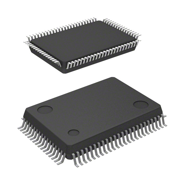
PACKAGE DIMENSIONS
Notes for Mounting the Surface Mount Type Package
The surface mount type packages are very susceptible to heat in reflow mounting and humidity absorbed in storage.
Therefore, before you perform reflow mounting, contact LAPIS SEMICONDUCTOR’s responsible sales person for the
product name, package name, pin number, package code and desired mounting conditions (reflow method, temperature
and times).
24/26
�FEDL610Q174-01
ML610Q174
REVISION HISTORY
Document No.
FEDL610Q174-01
Date
Oct 25, 2013
Page
Previous
Current
Edition
Edition
–
–
Description
Final edition 1
25/26
�FEDL610Q174-01
ML610Q174
NOTES
No copying or reproduction of this document, in part or in whole, is permitted without the consent of LAPIS
Semiconductor Co., Ltd.
The content specified herein is subject to change for improvement without notice.
The content specified herein is for the purpose of introducing LAPIS Semiconductor's products (hereinafter
"Products"). If you wish to use any such Product, please be sure to refer to the specifications, which can be
obtained from LAPIS Semiconductor upon request.
Examples of application circuits, circuit constants and any other information contained herein illustrate the
standard usage and operations of the Products. The peripheral conditions must be taken into account when
designing circuits for mass production.
Great care was taken in ensuring the accuracy of the information specified in this document. However, should
you incur any damage arising from any inaccuracy or misprint of such information, LAPIS Semiconductor
shall bear no responsibility for such damage.
The technical information specified herein is intended only to show the typical functions of and examples of
application circuits for the Products. LAPIS Semiconductor does not grant you, explicitly or implicitly, any
license to use or exercise intellectual property or other rights held by LAPIS Semiconductor and other parties.
LAPIS Semiconductor shall bear no responsibility whatsoever for any dispute arising from the use of such
technical information.
The Products specified in this document are intended to be used with general-use electronic equipment or
devices (such as audio visual equipment, office-automation equipment, communication devices, electronic
appliances and amusement devices).
The Products specified in this document are not designed to be radiation tolerant.
While LAPIS Semiconductor always makes efforts to enhance the quality and reliability of its Products, a
Product may fail or malfunction for a variety of reasons.
Please be sure to implement in your equipment using the Products safety measures to guard against the
possibility of physical injury, fire or any other damage caused in the event of the failure of any Product, such
as derating, redundancy, fire control and fail-safe designs. LAPIS Semiconductor shall bear no responsibility
whatsoever for your use of any Product outside of the prescribed scope or not in accordance with the
instruction manual.
The Products are not designed or manufactured to be used with any equipment, device or system which
requires an extremely high level of reliability the failure or malfunction of which may result in a direct threat
to human life or create a risk of human injury (such as a medical instrument, transportation equipment,
aerospace machinery, nuclear-reactor controller, fuel-controller or other safety device). LAPIS
Semiconductor shall bear no responsibility in any way for use of any of the Products for the above special
purposes. If a Product is intended to be used for any such special purpose, please contact a ROHM sales
representative before purchasing.
If you intend to export or ship overseas any Product or technology specified herein that may be controlled
under the Foreign Exchange and the Foreign Trade Law, you will be required to obtain a license or permit
under the Law.
Copyright 2013 LAPIS Semiconductor Co., Ltd.
26/26
�


 工商网监
湘ICP备2023018690号
工商网监
湘ICP备2023018690号