Dear customer
LAPIS Semiconductor Co., Ltd. ("LAPIS Semiconductor"), on the 1st day of October,
2020, implemented the incorporation-type company split (shinsetsu-bunkatsu) in which
LAPIS established a new company, LAPIS Technology Co., Ltd. (“LAPIS
Technology”) and LAPIS Technology succeeded LAPIS Semiconductor’s LSI business.
Therefore, all references to "LAPIS Semiconductor Co., Ltd.", "LAPIS Semiconductor"
and/or "LAPIS" in this document shall be replaced with "LAPIS Technology Co., Ltd."
Furthermore, there are no changes to the documents relating to our products other than
the company name, the company trademark, logo, etc.
Thank you for your understanding.
LAPIS Technology Co., Ltd.
October 1, 2020
�FEDL610Q409-05
Issue Date: May.23, 2014
ML610Q407/ML610Q408/ML61Q0409
8-bit Microcontroller with a Built-in LCD driver
GENERAL DESCRIPTION
ML610Q407/ML610Q408/ML610Q409 is a high-performance 8-bit CMOS microcontroller into which peripheral circuits, such
as synchronous serial port, UART, melody driver, RC oscillation type A/D converter, and LCD driver, are incorporated around
LAPIS Semiconductor-original 8-bit CPU nX-U8/100. ML610Q407/ML610Q408/ML610Q409 operates in both high/low-speed
mode and power-saving mode, it is most suitable for battery operated products.
The short TAT are entertained by offering MTP version ML610Q407(P)/ML610Q408(P)/ML610Q409(P).
ML610Q407P/ ML610Q408P/ML610Q409P support industrial temperature -40°C to +85°C, are added to the product lineup.
FEATURES
• CPU
− 8-bit RISC CPU (CPU name: nX-U8/100)
− Instruction system: 16-bit instructions
− Instruction set:
Transfer, arithmetic operations, comparison, logic operations, multiplication/division, bit
manipulations, bit logic operations, jump, conditional jump, call return stack manipulations, arithmetic
shift, and so on
− On-Chip debug function (MTP version only)
− Minimum instruction execution time
30.5 µs (@32.768 kHz system clock)
2µs (@500kHz system clock)
0.5µs(@2MHz system clock)
• Internal memory
− Internal 16KByte Flash ROM (8K×16 bits) (including unusable 1K Byte TEST area)
− Internal 1KByte Data RAM (1024×8 bits)
• Interrupt controller
− 1 non-maskable interrupt sources
Internal source: 1 (Watch dog timer)
− 27 maskable interrupt sources
Internal sources: 14 (SSIO0, SSIO1, Timer0, Timer1, Timer2, Timer3, UART0, Melody0, RC-A/D converter, PWM0,
TBC128Hz, TBC32Hz, TBC16Hz, TBC2Hz)
External sources: 13 (P00, P01, P02, P03, P04, P50, P51, P52, P53, P54, P55, P56, P57)
(One interrupt request is generated from P50 to P57 interrupt sources.)
• Time base counter
− Low-speed time base counter ×1 channel
Frequency compensation (Compensation range: Approx. −488ppm to +488ppm. Compensation accuracy: Approx.
0.48ppm)
− High-speed time base counter ×1 channel
•
Watchdog timer
− Non-maskable interrupt and reset
− Free running
− Overflow period: 4 types selectable (125ms, 500ms, 2s, and 8s)
• Timers
− 8 bits × 4 channels (Timer0-3: 16-bit x 2 configuration available by using Timer0-1 or Timer2-3)
− Clock frequency measurement mode (in one channel of 16-bit configuration using Timer2-3)
1/34
�FEDL610Q409-05
ML610Q407/ML610Q408/ML610Q409
• Capture
− Time base capture × 2 channels (4096 Hz to 32 Hz)
• PWM
− Resolution 16 bits × 1 channel
• Synchronous serial port
− Master/slave selectable × 2 channel
− LSB first/MSB first selectable
− 8-bit length/16-bit length selectable
• UART
− Half-Duplex Communication
− TXD/RXD × 1 channel
− Bit length, parity/no parity, odd parity/even parity, 1 stop bit/2 stop bits
− Positive logic/negative logic selectable
− Built-in baud rate generator
• Melody driver
− Scale: 29 types (Melody sound frequency: 508 Hz to 32.768 kHz)
− Tone length: 63 types
−Tempo: 15 types
− Buzzer output mode (4 output modes, 8 frequencies, 16 duty levels)
• RC oscillation type A/D converter
− 16-bit counter
− Time division × 2 channels
• General-purpose ports
− Input-only port × 5 channels (including secondary functions)
− Output-only port
ML610Q407: × 12 channels (including secondary functions)
ML610Q408: × 8 channels (including secondary functions)
ML610Q409: × 4 channels (including secondary functions)
− Input/output port × 22 channels (including secondary functions)
• LCD driver
− The number of segments
ML610Q407: 145 dots max. (29seg×5com, 30seg×4com, 31seg×3com, and 32seg×2com selectable)
ML610Q408: 165 dots max. (33seg×5com, 34seg×4com, 35seg×3com, and 36seg×2com selectable)
ML610Q409: 185 dots max. (37seg×5com, 38seg×4com, 39seg×3com, and 40seg×2com selectable)
− 1/1 to 1/5 duty
− 1/2(*), 1/3 bias (built-in bias generation circuit)
− Frame frequency selecable: approx. 64Hz, 73Hz, 85Hz, and 102Hz
− Bias voltage multiplying clock selectable (8 types)
− LCD drive stop mode, LCD display mode, all LCDs on mode, and all LCDs off mode selectable
− Programmable display allocation function
(*) 1/2 bias is supported by A version and D version
• Reset
− Reset through the RESET_N pin
− Power-on reset generation when powered on
− Reset when oscillation stop of the low-speed clock is detected (Not supported in A version)
− Reset by the watchdog timer (WDT) overflow
2/34
�FEDL610Q409-05
ML610Q407/ML610Q408/ML610Q409
• Clock
− Low-speed clock: Crystal oscillation (32.768 kHz)
(This LSI can not guarantee the operation withoug low-speed crystal oscillation clock)
− High-speed clock: Built-in RC oscillation (500 kHz, 2MHz)
• Power management
− HALT mode: Instruction execution by CPU is suspended (peripheral circuits are in operating states).
− STOP mode: Stop of low-speed oscillation and high-speed oscillation (Operations of CPU and peripheral circuits are
stopped.)
− High-speed Clock gear: The frequency of high-speed system clock can be changed by software (1/1, 1/2, 1/4, 1/8 of the
oscillation clock)
− Block Control Function: Resets and completely turns circuits of unused peripherals off.
• Guaranteed operating range
− Operating temperature: −20°C to +70°C (P version: −40°C to +85°C)
− Operating voltage: VDD = 1.25V to 3.6V
3/34
�FEDL610Q409-05
ML610Q407/ML610Q408/ML610Q409
• Product name – Supported Function
1/2
1/3
Low-speed
oscillation
stop detect reset
ML610Q407-xxxWA
-
Yes
Yes
-20°C to +70°C
Yes
ML610Q408-xxxWA
-
Yes
Yes
-20°C to +70°C
Yes
ML610Q409-xxxWA
-
Yes
Yes
-20°C to +70°C
Yes
ML610Q407P-xxxWA
-
Yes
Yes
-40°C to +85°C
Yes
ML610Q408P-xxxWA
-
Yes
Yes
-40°C to +85°C
Yes
LCD bias
- Chip (Die) -
Operating
temperature
Product availability
ML610Q409P-xxxWA
ML610Q407A- x x x WA
-
Yes
Yes
-40°C to +85°C
Yes
Yes
Yes
-
-20°C to +70°C
Yes
ML610Q408A-xxxWA
Yes
Yes
-
-20°C to +70°C
-
ML610Q409A-xxxWA
Yes
Yes
-
-20°C to +70°C
Yes
ML610Q407D-xxxWA
Yes
Yes
Yes
-20°C to +70°C
Yes
ML610Q408D-xxxWA
Yes
Yes
Yes
-20°C to +70°C
-
ML610Q409D-xxxWA
Yes
Yes
Yes
-20°C to +70°C
-
ML610Q407PA-xxxWA
Yes
Yes
-
-40°C to +85°C
Yes
ML610Q408PA-xxxWA
Yes
Yes
-
-40°C to +85°C
-
ML610Q409PA-xxxWA
Yes
Yes
-
-40°C to +85°C
-
ML610Q407PD-xxxWA
Yes
Yes
Yes
-40°C to +85°C
-
ML610Q408PD-xxxWA
Yes
Yes
Yes
-40°C to +85°C
-
ML610Q409PD-xxxWA
Yes
Yes
Yes
-40°C to +85°C
-
Operating
temperature
Product availability
1/2
1/3
Low-speed
oscillation
stop detect reset
ML610Q407-xxxTB
-
Yes
Yes
-20°C to +70°C
Yes
ML610Q408-xxxTB
-
Yes
Yes
-20°C to +70°C
Yes
ML610Q409-xxxTB
-
Yes
Yes
-20°C to +70°C
Yes
ML610Q407P-xxxTB
-
Yes
Yes
-40°C to +85°C
Yes
ML610Q408P-xxxTB
-
Yes
Yes
-40°C to +85°C
Yes
-100-pin plastic
TQFP -
LCD bias
ML610Q409P-xxxTB
-
Yes
Yes
-40°C to +85°C
Yes
ML610Q407A-xxxTB
Yes
Yes
-
-20°C to +70°C
-
ML610Q408A-xxxTB
Yes
Yes
-
-20°C to +70°C
-
ML610Q409A-xxxTB
Yes
Yes
-
-20°C to +70°C
-
ML610Q407D-xxxTB
Yes
Yes
Yes
-20°C to +70°C
-
ML610Q408D-xxxTB
Yes
Yes
Yes
-20°C to +70°C
-
ML610Q409D-xxxTB
Yes
Yes
Yes
-20°C to +70°C
-
ML610Q407PAxxxTB
Yes
Yes
-
-40°C to +85°C
-
ML610Q408PAxxxTB
Yes
Yes
-
-40°C to +85°C
-
ML610Q409PAxxxTB
Yes
Yes
-
-40°C to +85°C
-
ML610Q407PDxxxTB
Yes
Yes
Yes
-40°C to +85°C
-
ML610Q408PDxxxTB
Yes
Yes
Yes
-40°C to +85°C
-
ML610Q409PDxxxTB
Yes
Yes
Yes
-40°C to +85°C
-
xxx: ROM code number (xxx of the blank product is NNN)
Q: MTP version
P: Wide range temperature version (P version)
A: Low-speed clock oscillation stop detection reset is disabled always and LCD 1/2 bias supported version.(A
version)
D: LCD 1/2 bias supported version (D version)
WA: Chip (Die),
TB: TQFP
4/34
�FEDL610Q409-05
ML610Q407/ML610Q408/ML610Q409
BLOCK DIAGRAM
ML610Q407/ML610Q408/ML610Q409 Block Diagram
Figure 1 show the block diagram of the ML610Q407/ML610Q408/ML610Q409.
“*” indicates the secondary function of each port.
“(*1)”: 29seg×5com, 30seg×4com, 31seg×3com, and 32seg×2com selectable
“(*2)”: 33seg×5com, 34seg×4com, 35seg×3com, and 36seg×2com selectable
“(*3)”: 37seg×5com, 38seg×4com, 39seg×3com, and 40seg×2com selectable
CPU (nX-U8/100)
EPSW1~3
GREG
0~15
PSW
Timing
Controller
ALU
LR
DSR/CSR
EA
PC
Instruction
Register
Data-bus
VDD
VSS
RESET_N
TEST0
TEST1_N
ECSR1~3
SP
Instruction
Decoder
On-Chip
ICE
ELR1~3
Program
Memory
(MTP)
16Kbyte
BUS
Controller
INT
2
RAM
1Kbyte
RESET &
TEST
SSIO
×2
Interrupt
Controller
XT0
XT1
INT
1
OSC
LSCLK*
OUTCLK*
VDDL
IN0*
CS0*
RS0*
RT0*
CRT0*
RCM*
IN1*
CS1*
RS1*
RT1*
INT
4
WDT
TBC
RC-ADC
×2
INT
4
8bit Timer
×4
Display
Allocation
RAM
Display
register
320bit
SCK1*
SIN1*
SOUT1*
UART
RXD0*
TXD0*
PWM
PWM0*
INT
1
INT
1
Capture
×2
SCK0*
SIN0*
SOUT0*
INT
1
Power
INT
1
VPP
Melody
INT
6
GPIO
MD0*
P00 to P04
P20 to P22, P24
P30 to P35
P40 to P47
P50 to P57
P60 to P67 (ML610Q407)
P60 to P63 (ML610Q408)
LCD
Driver
LCD
BIAS
(*1)(*2)(*3)
COM0 to COM4
SEG0 to SEG31 (ML610Q407) (*1)
SEG0 to SEG35 (ML610Q408) (*2)
SEG0 to SEG39 (ML610Q409) (*3)
VL1, VL2, VL3
C1, C2
Figure 1 ML610Q407/ML610Q408/ML610Q409 Block Diagram
5/34
�FEDL610Q409-05
ML610Q407/ML610Q408/ML610Q409
PIN CONFIGURATION
76
77
78
79
80
81
82
83
84
85
86
87
88
89
90
91
92
93
94
95
96
97
98
99
100
(NC)
(NC)
SEG17
SEG16
SEG15
SEG14
SEG13
SEG12
SEG11
SEG10
SEG9
SEG8
SEG7
SEG6
SEG5
SEG4
SEG3
COM4/SEG2
COM3/SEG1
COM2/SEG0
COM1
COM0
C2
C1
(NC)
1
2
3
4
5
6
7
8
9
10
11
12
13
14
15
16
17
18
19
20
21
22
23
24
25
50
49
48
47
46
45
44
43
42
41
40
39
38
37
36
35
34
33
32
31
30
29
28
27
26
(NC)
P52
P51
P50
P40
P41
P42
P43
P44
P45
P46
P47
VDD
VSS
VDDL
(NC
XT0
XT1
RESET_N
TEST0
TEST1_N
VL1
VL2
VL3
(NC)
(NC)
VSS
P20
P21
P22
P24
P00
P01
P02
P03
P04
P30
P31
P34
P32
P33
P35
P57
P56
P55
P54
P53
VPP
(NC)
(NC)
75
74
73
72
71
70
69
68
67
66
65
64
63
62
61
60
59
58
57
56
55
54
53
52
51
(NC)
(NC)
P60
P61
P62
P63
P64
P65
P66
P67
SEG31
SEG30
SEG29
SEG28
SEG27
SEG26
SEG25
SEG24
SEG23
SEG22
SEG21
SEG20
SEG19
SEG18
(NC)
ML610Q407 TQFP100 Pin Layout
Note:
The assignment of the P30 to P35 are not in order.
Figure 2 ML610Q407 TQFP100 Pin Configuration
6/34
�FEDL610Q409-05
ML610Q407/ML610Q408/ML610Q409
76
77
78
79
80
81
82
83
84
85
86
87
88
89
90
91
92
93
94
95
96
97
98
99
100
(NC)
(NC)
SEG17
SEG16
SEG15
SEG14
SEG13
SEG12
SEG11
SEG10
SEG9
SEG8
SEG7
SEG6
SEG5
SEG4
SEG3
COM4/SEG2
COM3/SEG1
COM2/SEG0
COM1
COM0
C2
C1
(NC)
1
2
3
4
5
6
7
8
9
10
11
12
13
14
15
16
17
18
19
20
21
22
23
24
25
50
49
48
47
46
45
44
43
42
41
40
39
38
37
36
35
34
33
32
31
30
29
28
27
26
(NC)
P52
P51
P50
P40
P41
P42
P43
P44
P45
P46
P47
VDD
VSS
VDDL
(NC)
XT0
XT1
RESET_N
TEST0
TEST1_N
VL1
VL2
VL3
(NC)
(NC)
VSS
P20
P21
P22
P24
P00
P01
P02
P03
P04
P30
P31
P34
P32
P33
P35
P57
P56
P55
P54
P53
VPP
(NC)
(NC)
75
74
73
72
71
70
69
68
67
66
65
64
63
62
61
60
59
58
57
56
55
54
53
52
51
(NC)
(NC)
P60
P61
P62
P63
SEG35
SEG34
SEG33
SEG32
SEG31
SEG30
SEG29
SEG28
SEG27
SEG26
SEG25
SEG24
SEG23
SEG22
SEG21
SEG20
SEG19
SEG18
(NC)
ML610Q408 TQFP100 Pin Layout
Note:
The assignment of the P30 to P35 are not in order.
Figure 3 ML610Q408 TQFP100 Pin Configuration
7/34
�FEDL610Q409-05
ML610Q407/ML610Q408/ML610Q409
76
77
78
79
80
81
82
83
84
85
86
87
88
89
90
91
92
93
94
95
96
97
98
99
100
(NC)
(NC)
SEG17
SEG16
SEG15
SEG14
SEG13
SEG12
SEG11
SEG10
SEG9
SEG8
SEG7
SEG6
SEG5
SEG4
SEG3
COM4/SEG2
COM3/SEG1
COM2/SEG0
COM1
COM0
C2
C1
(NC)
1
2
3
4
5
6
7
8
9
10
11
12
13
14
15
16
17
18
19
20
21
22
23
24
25
50
49
48
47
46
45
44
43
42
41
40
39
38
37
36
35
34
33
32
31
30
29
28
27
26
(NC)
P52
P51
P50
P40
P41
P42
P43
P44
P45
P46
P47
VDD
VSS
VDDL
(NC)
XT0
XT1
RESET_N
TEST0
TEST1_N
VL1
VL2
VL3
(NC)
(NC)
VSS
P20
P21
P22
P24
P00
P01
P02
P03
P04
P30
P31
P34
P32
P33
P35
P57
P56
P55
P54
P53
VPP
(NC)
(NC)
75
74
73
72
71
70
69
68
67
66
65
64
63
62
61
60
59
58
57
56
55
54
53
52
51
(NC)
(NC)
SEG39
SEG38
SEG37
SEG36
SEG35
SEG34
SEG33
SEG32
SEG31
SEG30
SEG29
SEG28
SEG27
SEG26
SEG25
SEG24
SEG23
SEG22
SEG21
SEG20
SEG19
SEG18
(NC)
ML610Q409 TQFP100 Pin Layout
Note:
The assignment of the P30 to P35 are not in order.
Figure 4 ML610Q409 TQFP100 Pin Configuration
8/34
�FEDL610Q409-05
ML610Q407/ML610Q408/ML610Q409
66
65
64
63
62
61
60
59
58
57
56
55
54
53
52
51
50
49
48
47
46
45
P60
P61
P62
P63
P64
P65
P66
P67
SEG31
SEG30
SEG29
SEG28
SEG27
SEG26
SEG25
SEG24
SEG23
SEG22
SEG21
SEG20
SEG19
SEG18
ML610Q407 Chip Pin Layout & Dimension
67
68
69
70
71
72
73
74
75
76
77
78
79
80
81
82
83
84
85
86
87
88
1
2
3
4
5
6
7
8
9
10
11
12
13
14
15
16
17
18
19
20
21
22
XT1
RESET_N
TEST0
TEST1_N
VL1
VL2
VL3
44
43
42
41
40
39
38
37
36
35
34
33
32
31
30
29
28
27
26
25
24
23
P52
P51
P50
P40
P41
P42
P43
P44
P45
P46
P47
VDD
VSS
VDDL
XT0
VSS
P20
P21
P22
P24
P00
P01
P02
P03
P04
P30
P31
P34
P32
P33
P35
P57
P56
P55
P54
P53
VPP
SEG17
SEG16
SEG15
SEG14
SEG13
SEG12
SEG11
SEG10
SEG9
SEG8
SEG7
2.23mm
SEG6
SEG5
SEG4
SEG3
COM4/SEG2
COM3/SEG1
COM2/SEG0
COM1
COM0
C2
C1
2.27mm
Y
X
Note:
The assignment of the pads P30 to P35 are not in order.
Chip size: 2.27 mm × 2.23 mm
PAD count: 88 pins
Minimum PAD pitch: 80µm
PAD aperture: 70µm×70µm
Chip thickness: 350µm
Voltage of the rear side of chip: VSS level.
Figure 5 ML610Q407 Chip Layout & Dimension
9/34
�FEDL610Q409-05
ML610Q407/ML610Q408/ML610Q409
66
65
64
63
62
61
60
59
58
57
56
55
54
53
52
51
50
49
48
47
46
45
P60
P61
P62
P63
SEG35
SEG34
SEG33
SEG32
SEG31
SEG30
SEG29
SEG28
SEG27
SEG26
SEG25
SEG24
SEG23
SEG22
SEG21
SEG20
SEG19
SEG18
ML610Q408 Chip Pin Layout & Dimension
67
68
69
70
71
72
73
74
75
76
77
78
79
80
81
82
83
84
85
86
87
88
1
2
3
4
5
6
7
8
9
10
11
12
13
14
15
16
17
18
19
20
21
22
XT1
RESET_N
TEST0
TEST1_N
VL1
VL2
VL3
44
43
42
41
40
39
38
37
36
35
34
33
32
31
30
29
28
27
26
25
24
23
P52
P51
P50
P40
P41
P42
P43
P44
P45
P46
P47
VDD
VSS
VDDL
XT0
VSS
P20
P21
P22
P24
P00
P01
P02
P03
P04
P30
P31
P34
P32
P33
P35
P57
P56
P55
P54
P53
VPP
SEG17
SEG16
SEG15
SEG14
SEG13
SEG12
SEG11
SEG10
SEG9
SEG8
SEG7
2.23mm
SEG6
SEG5
SEG4
SEG3
COM4/SEG2
COM3/SEG1
COM2/SEG0
COM1
COM0
C2
C1
2.27mm
Y
X
Note:
The assignment of the pads P30 to P35 are not in order.
Chip size: 2.27 mm × 2.23 mm
PAD count: 88 pins
Minimum PAD pitch: 80µm
PAD aperture: 70µm×70µm
Chip thickness: 350µm
Voltage of the rear side of chip: VSS level.
Figure 6 ML610Q408 Chip Layout & Dimension
10/34
�FEDL610Q409-05
ML610Q407/ML610Q408/ML610Q409
66
65
64
63
62
61
60
59
58
57
56
55
54
53
52
51
50
49
48
47
46
45
SEG39
SEG38
SEG37
SEG36
SEG35
SEG34
SEG33
SEG32
SEG31
SEG30
SEG29
SEG28
SEG27
SEG26
SEG25
SEG24
SEG23
SEG22
SEG21
SEG20
SEG19
SEG18
ML610Q409 Chip Pin Layout & Dimension
67
68
69
70
71
72
73
74
75
76
77
78
79
80
81
82
83
84
85
86
87
88
1
2
3
4
5
6
7
8
9
10
11
12
13
14
15
16
17
18
19
20
21
22
XT1
RESET_N
TEST0
TEST1_N
VL1
VL2
VL3
44
43
42
41
40
39
38
37
36
35
34
33
32
31
30
29
28
27
26
25
24
23
P52
P51
P50
P40
P41
P42
P43
P44
P45
P46
P47
VDD
VSS
VDDL
XT0
VSS
P20
P21
P22
P24
P00
P01
P02
P03
P04
P30
P31
P34
P32
P33
P35
P57
P56
P55
P54
P53
VPP
SEG17
SEG16
SEG15
SEG14
SEG13
SEG12
SEG11
SEG10
SEG9
SEG8
SEG7
2.23mm
SEG6
SEG5
SEG4
SEG3
COM4/SEG2
COM3/SEG1
COM2/SEG0
COM1
COM0
C2
C1
2.27mm
Y
X
Note:
The assignment of the pads P30 to P35 are not in order.
Chip size: 2.27 mm × 2.23 mm
PAD count: 88 pins
Minimum PAD pitch: 80 µm
PAD aperture: 70 µm×70 µm
Chip thickness: 350 µm
Voltage of the rear side of chip: VSS level.
Figure 7 ML610Q409 Chip Layout & Dimension
11/34
�FEDL610Q409-05
ML610Q407/ML610Q408/ML610Q409
ML610Q407/ML610Q408/ML610Q409 Pad Coordinates
Table 1 ML610Q407/ML610Q408/ML610Q409 Pad Coordinates
Chip Center: X=0,Y=0
(*1)
PAD
No.
Pad
Name
1
P52
2
P51
3
P50
4
P40
5
P41
6
P42
7
P43
8
P44
9
P45
10
P46
11
P47
12
VDD
13
VSS
14
VDDL
15
XT0
16
XT1
17
RESET_N
18
TEST0
19
TEST1_N
20
VL1
21
VL2
22
VL3
23
C0
24
C1
25
COM0
26
COM1
27
COM2/SEG0
28
COM3/SEG1
29
COM4/SEG2
30
SEG3
31
SEG4
32
SEG5
33
SEG6
34
35
SEG7
SEG8
36
SEG9
37
SEG10
38
SEG11
39
SEG12
40
SEG13
41
SEG14
42
SEG15
43
SEG16
44
SEG17
45
SEG18
46
SEG19
47
SEG20
48
SEG21
ML610Q407/8/9
X (µm)
Y (µm)
-853
-1009
-773
-1009
-693
-1009
-613
-1009
-533
-1009
-453
-1009
-373
-1009
-293
-1009
-213
-1009
-133
-1009
-53
-1009
27
-1009
107
-1009
187
-1009
267
-1009
427
-1009
507
-1009
587
-1009
667
-1009
747
-1009
827
-1009
907
-1009
1029
-840
1029
-760
1029
-680
1029
-600
1029
-520
1029
-440
1029
-360
1029
-280
1029
-200
1029
-120
1029
-40
1029
40
1029
120
1029
200
1029
280
1029
360
1029
440
1029
520
1029
600
1029
680
1029
760
1029
840
855
1009
775
1009
695
1009
615
1009
PAD
No.
Pad
Name
49
SEG22
50
SEG23
51
SEG24
52
SEG25
53
SEG26
54
SEG27
55
SEG28
56
SEG29
57
SEG30
58
SEG31
59
60
61
62
63
64
65
66
P67 (*1)
SEG32 (*2)(*3)
P66
P65 (*1)
SEG34 (*2)(*3)
P64 (*1)
SEG35 (*2)(*3)
P63 (*1)(*2)
SEG36 (*3)
P62 (*1)(*2)
SEG37 (*3)
1009
1009
1009
1009
1009
1009
1009
1009
1009
1009
-295
1009
-375
1009
-455
1009
-535
1009
-615
1009
-695
1009
-775
1009
-885
1009
-1029
-1029
--1029
-1029
-1029
-1029
-1029
-1029
-1029
-1029
-1029
-1029
-1029
-1029
-1029
-1029
-1029
-1029
-1029
-1029
-1029
-1029
850
770
690
610
530
430
350
270
190
110
30
-50
-130
-210
-290
-370
-450
-530
-610
-690
-770
-850
(*1)(*2)
SEG38 (*3)
P60
535
455
375
295
215
135
55
-25
-105
-185
(*1)
SEG33 (*2)(*3)
P61
ML610Q407/8/9
X (µm)
Y (µm)
(*1)(*2)
SEG39 (*3)
67
VSS
68
P20
69
P21
70
P22
71
P24
72
P00
73
P01
74
75
P02
P03
76
P04
77
P30
78
P31
79
P34
80
P32
81
P33
82
P35
83
P57
84
P56
85
P55
86
P54
87
P53
88
VPP
ML610Q407 pad name, (*2) ML610Q408 pad name, (*3) ML610Q409 pad name
12/34
�FEDL610Q409-05
ML610Q407/ML610Q408/ML610Q409
PIN LIST
Primary function
PIN
No.
PAD
No.
Pin name
I/O
Function
14,77
13
13,67
12
Vss
VDD
⎯
⎯
15
14
VDDL
⎯
98
88
VPP
⎯
22
20
VL1
⎯
23
21
VL2
⎯
24
22
VL3
⎯
27
23
C1
⎯
28
24
C2
⎯
Negative power supply pin
Positive power supply pin
Power supply pin for internal logic
(internally generated)
Power supply pin for Flash ROM
Power supply pin for LCD bias
(internally generated or connected
to positive power supply pin)(*2)
Power supply pin for LCD bias
(internally generated or connected
to positive power supply pin)(*2)
Power supply pin for LCD bias
(internally generated)
Capacitor connection pin for LCD
bias generation
Capacitor connection pin for LCD
bias generation
Test pin
20
18
TEST0
I/O
21
19
17
18
19
17
15
16
TEST1_N
RESET_N
XT0
XT1
I
I
I
O
82
72
P00/EXI0/
CAP0
I
83
73
P01/EXI1/
CAP1
I
84
74
P02/EXI2/
RXD0
I
85
75
P03/EXI3
I
86
76
P04/EXI4/
T02P0CK
I
78
79
80
81
68
69
70
71
P20/LED0
P21/LED1
P22/LED2
P24/LED4
87
77
88
Secondary function or Tertiary function
Secondary
/Tertiary
⎯
⎯
Pin name
I/O
Function
⎯
⎯
⎯
⎯
⎯
⎯
⎯
⎯
⎯
⎯
⎯
⎯
⎯
⎯
⎯
⎯
⎯
⎯
⎯
⎯
⎯
⎯
⎯
⎯
⎯
⎯
⎯
⎯
⎯
⎯
⎯
⎯
⎯
⎯
⎯
⎯
⎯
⎯
⎯
⎯
⎯
⎯
⎯
⎯
⎯
⎯
⎯
⎯
⎯
⎯
⎯
⎯
⎯
⎯
⎯
⎯
⎯
⎯
⎯
⎯
⎯
⎯
⎯
⎯
⎯
⎯
⎯
⎯
⎯
⎯
⎯
⎯
⎯
⎯
O
O
O
O
Test pin
Reset input pin
Low-speed clock oscillation pin
Low-speed clock oscillation pin
Input port,
External interrupt,
Capture 0 input
Input port,
External interrupt,
Capture 1 input
Input port,
External interrupt,
UART0 received data
Input port,
External interrupt
Input port,
Timer 0/Timer 2/PWM0 external
clock input
External interrupt
Output port
Output port
Output port
Output port
Secondary
Secondary
Secondary
Secondary
LSCLK
OUTCLK
MD0
PWM0
O
O
O
O
P30
I/O
Input/output port
Secondary
IN0
I
78
P31
I/O
Input/output port
Secondary
CS0
O
89
79
P34
I/O
Input/output port
Secondary
RCT0
O
90
80
P32
I/O
Input/output port
Secondary
RS0
O
91
81
P33
I/O
Input/output port
Secondary
RT0
O
92
82
P35
I/O
Input/output port
Secondary
RCM
O
Low-speed clock output
High-speed clock output
Melody 0 output
PWM0 output
RC type ADC0 oscillation input
pin
RC type ADC0 reference
capacitor connection pin
RC type ADC0
resistor/capacitor sensor
connection pin
RC type ADC0 reference
resistor connection pin
RC type ADC0 measurement
resistor sensor connection pin
RC type ADC oscillation
monitor
13/34
�FEDL610Q409-05
ML610Q407/ML610Q408/ML610Q409
Primary function
PIN
No.
PAD
No.
Pin name
I/O
5
4
P40
I/O
Input/output port
6
5
P41
I/O
Input/output port
7
6
P42
I/O
Input/output port
8
7
P43
I/O
Input/output port
9
8
P44/
T02P0CK
I/O
Input/output port,
Timer 0/Timer 2/PWM0 external
clock input
P45/T13CK
I/O
10
11
9
10
P46
I/O
Function
Input/output port,
Timer 1/Timer 3 external clock
input
Input/output port
Secondary function or Tertiary function
Secondary
/Tertiary
Secondary
Tertiary
Secondary
Pin name
I/O
Function
⎯
SIN0
⎯
⎯
I
⎯
Tertiary
SCK0
I/O
Secondary
Tertiary
Secondary
Tertiary
RXD0
SOUT0
TXD0
PWM0
I
O
O
O
Secondary
IN1
I
Tertiary
SIN0
I
Secondary
CS1
O
⎯
SSIO0 data input
⎯
SSIO0 synchronous clock
input/output
UART data input
SSIO0 data output
UART data output
PWM0 output
RC type ADC1 oscillation input
pin
SSIO0 data input
RC type ADC1 reference
capacitor connection pin
Tertiary
SCK0
I/O
Secondary
RS1
O
Tertiary
SOUT0
O
12
11
P47
I/O
Input/output port
Secondary
RT1
O
4
3
P50/EXI8
I/O
Input/output port,
External interrupt
3
2
P51/EXI8
I/O
Input/output port,
External interrupt
Secondary
Tertiary
Secondary
MD0
SIN1
⎯
O
I
⎯
Tertiary
SCK1
I/O
2
1
P52/EXI8
I/O
Secondary
Tertiary
⎯
SOUT1
⎯
O
97
87
P53/EXI8
I/O
⎯
⎯
⎯
96
86
P54/EXI8
I/O
Secondary
Tertiary
Secondary
95
85
P55/EXI8
I/O
⎯
SIN1
⎯
⎯
I
⎯
Tertiary
SCK1
I/O
94
84
P56/EXI8
I/O
Secondary
Tertiary
⎯
SOUT1
⎯
O
93
83
P57/EXI8
I/O
⎯
⎯
⎯
Input/output port,
External interrupt
Input/output port,
External interrupt
Input/output port,
External interrupt
Input/output port,
External interrupt
Input/output port,
External interrupt
Input/output port,
External interrupt
SSIO0 synchronous clock
input/output
RC type ADC1 reference
resistor connection pin
SSIO0 data output
RC type ADC1 measurement
resistor sensor connection pin
Melody 0 output
SSIO1 data input
⎯
SSIO1 synchronous clock
input/output
⎯
SSIO1 data output
⎯
⎯
SSIO1 data input
⎯
SSIO1 synchronous clock
input/output
⎯
SSIO1 data output
⎯
14/34
�FEDL610Q409-05
ML610Q407/ML610Q408/ML610Q409
PIN
No.
PAD
No.
29
30
25
26
31
27
32
28
33
29
34
35
36
37
38
39
40
41
42
43
44
45
46
47
48
52
53
54
55
56
57
58
59
60
61
62
63
64
65
30
31
32
33
34
35
36
37
38
39
40
41
42
43
44
45
46
47
48
49
50
51
52
53
54
55
56
57
58
66
59
67
60
68
61
69
62
70
63
71
64
72
65
73
66
Primary function
Secondary function or Tertiary function
Secondary/
Tertiary
⎯
⎯
Pin
name
⎯
⎯
I/O
Function
⎯
⎯
⎯
⎯
⎯
⎯
⎯
⎯
⎯
⎯
⎯
LCD common/segment pin
⎯
⎯
⎯
⎯
LCD segment pin
LCD segment pin
LCD segment pin
LCD segment pin
LCD segment pin
LCD segment pin
LCD segment pin
LCD segment pin
LCD segment pin
LCD segment pin
LCD segment pin
LCD segment pin
LCD segment pin
LCD segment pin
LCD segment pin
LCD segment pin
LCD segment pin
LCD segment pin
LCD segment pin
LCD segment pin
LCD segment pin
LCD segment pin
LCD segment pin
LCD segment pin
LCD segment pin
LCD segment pin
LCD segment pin
LCD segment pin
LCD segment pin
Output port
LCD segment pin
Output port
LCD segment pin
Output port
LCD segment pin
Output port
LCD segment pin
Output port
LCD segment pin
Output port
LCD segment pin
Output port
LCD segment pin
Output port
LCD segment pin
⎯
⎯
⎯
⎯
⎯
⎯
⎯
⎯
⎯
⎯
⎯
⎯
⎯
⎯
⎯
⎯
⎯
⎯
⎯
⎯
⎯
⎯
⎯
⎯
⎯
⎯
⎯
⎯
⎯
⎯
⎯
⎯
⎯
⎯
⎯
⎯
⎯
⎯
⎯
⎯
⎯
⎯
⎯
⎯
⎯
⎯
⎯
⎯
⎯
⎯
⎯
⎯
⎯
⎯
⎯
⎯
⎯
⎯
⎯
⎯
⎯
⎯
⎯
⎯
⎯
⎯
⎯
⎯
⎯
⎯
⎯
⎯
⎯
⎯
⎯
⎯
⎯
⎯
⎯
⎯
⎯
⎯
⎯
⎯
⎯
⎯
⎯
⎯
⎯
⎯
⎯
⎯
⎯
⎯
⎯
⎯
⎯
⎯
⎯
⎯
⎯
⎯
⎯
⎯
⎯
⎯
⎯
⎯
⎯
⎯
⎯
⎯
⎯
⎯
⎯
⎯
⎯
⎯
⎯
⎯
⎯
⎯
⎯
⎯
⎯
⎯
⎯
⎯
⎯
⎯
⎯
⎯
⎯
⎯
⎯
⎯
⎯
⎯
⎯
⎯
⎯
⎯
⎯
⎯
⎯
⎯
⎯
⎯
⎯
⎯
⎯
⎯
⎯
⎯
⎯
⎯
⎯
⎯
⎯
⎯
⎯
⎯
⎯
⎯
⎯
⎯
⎯
⎯
⎯
⎯
⎯
⎯
⎯
⎯
⎯
⎯
⎯
⎯
⎯
⎯
Pin name
I/O
Function
COM0
COM1
COM2/
SEG0
COM3/
SEG1
COM4/
SEG2
SEG3
SEG4
SEG5
SEG6
SEG7
SEG8
SEG9
SEG10
SEG11
SEG12
SEG13
SEG14
SEG15
SEG16
SEG17
SEG18
SEG19
SEG20
SEG21
SEG22
SEG23
SEG24
SEG25
SEG26
SEG27
SEG28
SEG29
SEG30
SEG31
P67(*2)
SEG32(*3)
P66(*2)
SEG33(*3)
P65(*2)
SEG34(*3)
P64(*2)
SEG35(*3)
P63(*4)
SEG36(*5)
P62(*4)
SEG37(*5)
P61(*4)
SEG38(*5)
P60(*4)
SEG39(*5)
O
O
LCD common pin
LCD common pin
O
LCD common/segment pin
⎯
O
LCD common/segment pin
O
O
O
O
O
O
O
O
O
O
O
O
O
O
O
O
O
O
O
O
O
O
O
O
O
O
O
O
O
O
O
O
O
O
O
O
O
O
O
O
O
O
O
O
O
O
1
(* ) Internally generated, or connect to either positive power supply pin (VDD) or power supply pin for internal logic
(VDDL). For details, see “Chapter 22 LCD Drivers. In the user’s manual”
2
(* ) Pin for ML610Q407/ML610Q408.
3
(* ) Pin for ML610Q409.
4
(* ) Pin for ML610Q407.
5
(* ) Pin for ML610Q408/ML610Q409.
15/34
�FEDL610Q409-05
ML610Q407/ML610Q408/ML610Q409
PIN DESCRIPTION
Pin name
I/O
Description
Primary/
Secondary/
Tertiary
Logic
System
Reset input pin. When this pin is set to a “L” level, system reset mode is
—
Negative
set and the internal section is initialized. When this pin is set to a “H” level
subsequently, program execution starts. A pull-up resistor is internally
connected.
XT0
I Crystal connection pin for low-speed clock.
—
—
XT1
O A 32.768 kHz crystal oscillator (see measuring circuit 1) is connected to
—
—
this pin. Capacitors CDL and CGL are connected across this pin and VSS .
LSCLK
O Low-speed clock output pin. This pin is used as the secondary function of Secondary
—
the P20 pin.
OUTCLK
O High-speed clock output pin. This pin is used as the secondary function of Secondary
—
the P21 pin.
General-purpose input port
RESET_N
I
General-purpose input port.
Since these pins have secondary functions, the pins cannot be used as a
port when the secondary functions are used.
General-purpose output port
P20-P22,P24 O General-purpose output port.
Since these pins have secondary functions, the pins cannot be used as a
port when the secondary functions are used.
General-purpose input/output port
P30-P35
I/O General-purpose input/output port.
Since these pins have secondary functions, the pins cannot be used as a
port when the secondary functions are used.
P40-P47
I/O General-purpose input/output port.
Since these pins have secondary functions, the pins cannot be used as a
port when the secondary functions are used.
P50-P57
I/O General-purpose input/output port.
Since these pins have secondary functions, the pins cannot be used as a
port when the secondary functions are used.
P60-P63
O General-purpose input/output port.
These pins are for the ML610Q407/ ML610Q408, but are not provided in
the ML610Q409.
P64-P67
O General-purpose input/output port.
These pins are for the ML610Q407, but are not provided in the
ML610Q409.
P00-P04
I
Primary
Positive
Primary
Positive
Primary
Positive
Primary
Positive
Primary
Positive
Primary
Positive
Primary
Positive
16/34
�FEDL610Q409-05
ML610Q407/ML610Q408/ML610Q409
Pin name
Primary/
Secondary/
Tertiary
Logic
Secondary
Positive
Primary/
Secondary
Positive
Tertiary
—
Tertiary
Positive
Tertiary
Positive
Secondary
—
Secondary
Positive
Secondary
Positive
Tertiary
Positive
Primary
—
External maskable interrupt input pins. Interrupt enable and edge
selection can be performed for each bit by software. These pins are used
as the primary functions of the P00-P04 pins.
External maskable interrupt input pins. Interrupt enable and edge
selection can be performed for each bit by software. These pins are used
as the primary functions of the P50-P57 pins.
Primary
Positive/
negative
Primary
Positive/
negative
Capture trigger input pins. The value of the time base counter is captured
in the register synchronously with the interrupt edge selected by software.
These pins are used as the primary functions of the P00 pin(CAP0) and
P01 pin(CAP1).
Primary
Positive/
negative
Positive/
negative
I/O
UART
TXD0
O
RXD0
I
Description
UART data output pin. This pin is used as the secondary function of the
P43 pin.
UART data input pin. This pin is used as the secondary function of the
P42 or the primary function of the P02 pin.
Synchronous serial (SSIO)
SCK0
SIN0
SOUT0
SCK1
SIN1
SOUT1
PWM
PWM0
T02P0CK
I/O Synchronous serial clock input/output pin. This pin is used as the tertiary
function of the P41 or P45 pin.
I Synchronous serial data input pin. This pin is used as the tertiary function
of the P40 or P44 pin.
O Synchronous serial data output pin. This pin is used as the tertiary
function of the P42 or P46 pin.
I/O Synchronous serial clock input/output pin. This pin is used as the
secondary function of the P51 or P55 pin.
I Synchronous serial data input pin. This pin is used as the secondary
function of the P50 or P54.
O Synchronous serial data output pin. This pin is used as the secondary
function of the P52 or P56pin.
O
I
External interrupt
EXI0-4
I
EXI8
I
Capture
CAP0
I
CAP1
I
Timer
T02P0CK
T13CK
I
I
PWM0 output pin. This pin is used as the tertiary function of the P43 or
P34 pin.
PWM0 external clock input pin. This pin is used as the primary function of
the P44 pin.
External clock input pin used for Timer 0 and Timer 2. The clock for this
timer is selected by software. This pin is used as the primary function of
the P44 pin.
External clock input pin used both Timer 1 and Timer 3. The clock for this
timer is selected by software. This pin is used as the primary function of
the P45 pin.
Melody
MD0
O
Melody/Buzzer signal output pin. This pin is used as the secondary
function of the P22 pin and P50 pin.
LED drive
LED0-2,4
O
Nch open drain output pins to drive LED.
Primary
Primary
—
Primary
—
Secondary Positive/
negative
Primary
Positive/
negative
17/34
�FEDL610Q409-05
ML610Q407/ML610Q408/ML610Q409
Pin name
I/O
Description
RC oscillation type A/D converter
IN0
I Channel 0 oscillation input pin. This pin is used as the secondary function
of the P30 pin.
CS0
O Channel 0 reference capacitor connection pin. This pin is used as the
secondary function of the P31 pin.
RCT0
O Resistor/capacitor sensor connection pin of Channel 0 for measurement.
This pin is used as the secondary function of the P33 pin.
RS0
O This pin is used as the secondary function of the P32 pin which is the
reference resistor connection pin of Channel 0.
RT0
O Resistor sensor connection pin of Channel 0 for measurement. This pin is
used as the secondary function of the P34 pin.
RCM
O RC oscillation monitor pin. This pin is used as the secondary function of
the P35 pin.
IN1
I Oscillation input pin of Channel 1. This pin is used as the secondary
function of the P44 pin.
CS1
O Reference capacitor connection pin of Channel 1. This pin is used as the
secondary function of the P45 pin.
RS1
O Reference resistor connection pin of Channel 1. This pin is used as the
secondary function of the P46 pin.
RT1
O Resistor sensor connection pin for measurement of Channel 1. This pin is
used as the secondary function of the P47 pin.
LCD drive signal
COM0-4
O Common output pins.
SEG0-31
O Segment output pins.
Segment output pin. These pins are for the ML610Q408/ML610Q409, but
are not provided in the ML610Q407.
SEG36-39
O Segment output pin. These pins are for the ML610Q409, but are not
provided in the ML610Q407/ML610Q408.
LCD driver power supply
VL1
— Power supply pins for LCD bias (internally generated or positive power
VL2
— supply pin connected ). Depending on LCD Bias setting and VDD voltage
level, VDD or VDDL or capacitor is connected. For details of the connection
VL3
— method, see user’s manual.
C1
— Power supply pins for LCD bias (internally generated). Capacitors C12 is
connected between C1 and C2.
C2
—
For testing
TEST
I/O Input/output pin for testing. A pull-down resistor is internally connected.
SEG32-35
O
Power supply
VSS
—
VDD
—
VDDL
—
VPP
—
Negative power supply pin.
Positive power supply pin for I/O, internal regulator, battery low detector,
and power-on reset.
Positive power supply pin (internally generated) for internal logic.
Capacitor CL (see Appendix C measuring circuit 1) is connected between
this pin and VSS.
Power supply pin for programming Flash ROM. A pull-down resistor is
internally connected.
Primary/
Secondary/
Tertiary
Secondary
Secondary
Secondary
Secondary
Secondary
Secondary
Secondary
Secondary
Secondary
Secondary
Logic
—
—
—
—
—
—
—
—
—
—
—
—
—
—
—
—
—
—
—
—
—
—
—
—
—
—
—
—
—
—
—
—
—
—
—
—
—
—
18/34
�FEDL610Q409-05
ML610Q407/ML610Q408/ML610Q409
TERMINATION OF UNUSED PINS
Table 2 shows methods of terminating the unused pins.
Table 2
Pin
VPP
VL1, VL2, VL3
C1, C2
RESET_N
TEST0
TEST1_N
P00 to P04
P20 to P22, P24
P30 to P35
P40 to P47
P50 to P57
P60 to P67
COM0 to 4
SEG0 to 39
Termination of Unused Pins
Recommended pin termination
Open
Open
Open
Open
Open
Open
VDD or VSS
Open
Open
Open
Open
Open
Open
Open
Note:
It is recommended to set the unused input ports and input/output ports to the inputs with pull-down resistors/pull-up resistors or
the output mode since the supply current may become excessively large if the pins are left open in the high impedance input
setting.
19/34
�FEDL610Q409-05
ML610Q407/ML610Q408/ML610Q409
ELECTRICAL CHARACTERISTICS
ABSOLUTE MAXIMUM RATINGS
(VSS = 0V)
Parameter
Power supply voltage 1
Symbol
Condition
Rating
Unit
VDD
Ta = 25°C
−0.3 to +4.6
V
Power supply voltage 2
VPP
Ta = 25°C
−0.3 to +9.5
V
Power supply voltage 3
VDDL
Ta = 25°C
−0.3 to +3.6
V
Power supply voltage 4
VL1
Ta = 25°C
−0.3 to +2.0
V
Power supply voltage 5
VL2
Ta = 25°C
−0.3 to +4.0
V
Power supply voltage 6
VL3
Ta = 25°C
−0.3 to +6.0
V
Input voltage
VIN
Ta = 25°C
−0.3 to VDD+0.3
V
Output voltage
VOUT
Ta = 25°C
−0.3 to VDD+0.3
V
Output current 1
IOUT1
Port3–6, Ta = 25°C
−12 to +11
mA
Output current 2
IOUT2
Port2, Ta = 25°C
−12 to +20
mA
Power dissipation
PD
Ta = 25°C
0.9
W
Storage temperature
TSTG
⎯
−55 to +150
°C
RECOMMENDED OPERATING CONDITIONS
(VSS = 0V)
Parameter
Symbol
Condition
Range
non-P version
P version
fOP = 30k to 625kHz
−20 to +70
−40 to +85
1.25 to 3.6
fOP = 30k to 2.5MHz
VDD = 1.25 to 3.6V
VDD = 1.8 to 3.6V
1.8 to 3.6
30k to 625k
30k to 2.5M
CL
⎯
0.47±30%
µF
Ca, b, c
⎯
0.1±30%
µF
C12
⎯
0.47±30%
µF
Operating temperature
TOP
Operating voltage
VDD
Operating frequency (CPU)
fOP
Capacitor externally connected to
VDDL pin
Capacitors externally connected to
VL1, 2, 3 pins
Capacitors externally connected
across C1 and C2 pins
Unit
°C
V
Hz
CLOCK GENERATION CIRCUIT OPERATING CONDITIONS
(VSS = 0V)
Parameter
Low-speed crystal oscillation
frequency
Recommended equivalent series
resistance value of low-speed
crystal oscillation
Low-speed crystal oscillation
external capacitor
Symbol
Condition
fXTL
Rating
Unit
Min.
Typ.
Max.
⎯
⎯
32.768k
⎯
Hz
RL
⎯
⎯
⎯
40k
Ω
⎯
12
⎯
CDL/CGL
CL=6pF of crystal
oscillation
CL=9pF of crystal
oscillation
CL=12pF of
crystal oscillation
⎯
18
⎯
⎯
24
⎯
pF
20/34
�FEDL610Q409-05
ML610Q407/ML610Q408/ML610Q409
OPERATING CONDITIONS OF FLASH ROM
Parameter
Operating temperature
Symbol
TOP
VDD
VDDL
VPP
CEP
YDR
Operating voltage
erase/program cycles
Data retention
*1
Condition
At write/erase
*1
At write/erase
*1
At write/erase
*1
At write/erase
⎯
⎯
Range
0 to +40
2.75 to 3.6
2.5 to 2.75
7.7 to 8.3
80
10
(VSS = 0V)
Unit
°C
V
cycles
years
: Those voltages must be supplied to VDDL pin and VPP pin when programming and eraseing Flash ROM.
VPP pin has an internal pulldown resister.
DC CHARACTERISTICS (1/5)
(VDD = 1.25 to 3.6V, VSS = 0V, Ta = −20 to +70°C, Ta = −40 to +85°C for P version, unless otherwise specified)
Measuring
Rating
Parameter
Symbol
Condition
Unit
circuit
Min.
Typ.
Max.
Typ.
Typ.
500
Ta = 25°C
+10%
−10%
VDD = 1.25
kHz
to 3.6V
Typ.
Typ.
3
500
*
+25%
−25%
500kHz/2MHz RC oscillation
fRC
frequency
Typ.
Typ.
2.0
Ta = 25°C
+10%
−10%
VDD = 1.80
MHz
to 3.6V
Typ.
Typ.
3
2.0
*
+25%
−25%
Low-speed crystal oscillation
⎯
⎯
0.6
2
s
TXTL
2
1
start time*
500kHz/2MHz RC oscillation
⎯
⎯
⎯
0.3
µs
TRC
start time
Low-speed oscillation stop
TSTOP
⎯
12
16.4
41
ms
*1
detect time
Reset pulse width
PRST
⎯
200
⎯
⎯
µs
Reset noise elimination
⎯
⎯
⎯
0.3
PNRST
pulse width
Power-on reset activation
⎯
⎯
⎯
10
ms
TPOR
power rise time
1
* : When low-speed crystal oscillation stops for a duration more than the low-speed oscillation stop detect time, the system is
reset to shift to system reset mode.
2
* : 32.768KHz Crystal resonator DT-26 (Load capacitance 6pF) (made by KDS:DAISHINKU CORP.) is used (CGL=CDL=6pF).
3
* : Recommended operating temperature (Ta = −20 to +70°C, Ta = −40 to +85°C for P version)
VIL1
RESET_N
VIL1
PRST
Reset pulse width (PRST)
0.9xVDD
VDD
0.1xVDD
TPOR
Power-on reset activation power rise time (TPOR )
21/34
�FEDL610Q409-05
ML610Q407/ML610Q408/ML610Q409
DC CHARACTERISTICS (2/5)
(VDD = 1.25 to 3.6V, VSS = 0V, Ta = −20 to +70°C, Ta = −40 to +85°C for P version, unless otherwise specified)
Measuring
Rating
Parameter
Symbol
Condition
Unit
circuit
Min.
Typ.
Max.
VDDL voltage
VDDL
fOP = 30k to 625kHz
fOP = 30k to 2.5MHz
1.1
1.35
1.2
1.5
1.3
1.65
VDDL temperature
1
VDD = 3.0V
⎯
-1
⎯
mV/°C
∆VDDL
1
deviation *
VDDL voltage
∆VDDL
⎯
⎯
5
20
mV/V
1
dependency *
1
* :VDDL can not exceed VDD level. The maximum VDDL becomes VDD level when the VDDL calculated by the temperature
deviation and voltage dependency is going to exceed the VDD level.
22/34
�FEDL610Q409-05
ML610Q407/ML610Q408/ML610Q409
DC CHARACTERISTICS (3/5)
Parameter
Supply current 1
Supply current 2
Supply current 3
Supply current
4-1
Supply current
4-2
Symbol
IDD1
IDD2
IDD3
IDD4-1
IDD4-2
(VDD = 3.0V, VSS = 0V, Ta = −20 to +70°C, Ta = −40 to +85°C for P version)
Measuring
Rating
Condition
Unit
circuit
Min.
Typ.
Max.
CPU: In STOP state.
Low-speed/high-speed
RC500kHz/2MHz oscillation:
stopped.
CPU: In HALT state (LTBC and WDT
3 4
are Operating).* *
High-speed 500kHz/2MHz
oscillation: Stopped.
6
LCD and BIAS circuits: Operating. *
CPU: In 32.768kHz operating
1 3
state.* *
High-speed 500kHz/2MHz
oscillation: Stopped.
2
LCD and BIAS circuits: Operating. *
CPU: In RC 500kHz operating state.
2
LCD and BIAS circuits: Operating. *
CPU: In RC 2MHz operating state.
2
LCD and BIAS circuits: Operating. *
Ta= 25°C
⎯
0.4
0.8
µA
5
*
⎯
⎯
8
Ta= 25°C
⎯
0.9
1.8
µA
5
*
⎯
⎯
9
Ta= 25°C
⎯
5
8
µA
5
*
⎯
⎯
15
Ta= 25°C
⎯
70
100
*
⎯
⎯
120
Ta= 25°C
⎯
280
350
1
µA
5
µA
5
*
⎯
⎯
400
1
* : When the CPU operating rate is 100% (No HALT state).
2
* : All SEGs: off waveform, No LCD panel load, 1/3 bias, 1/3 duty, Frame frequency: Approx. 64 Hz, Bias voltage multiplying
clock: 1/128 LSCLK (256Hz)
3
* : 32.768KHz Crystal resonator DT-26 (Load capacitance 6pF) (made by KDS:DAISHINKU CORP.) is used (CGL=CDL=6pF)
4
* : Significant bits of BLKCON0~BLKCON4 registers except DLCD bit on BLKCON4 are all “1”.
5
* : Recommended operating temperature (Ta = −20 to +70°C, Ta = −40 to +85°C for P version)
6
* : LCD Stop mode, 1/3 bias, Bias voltage multiplying clock: 1/128 LSCLK (256Hz)
23/34
�FEDL610Q409-05
ML610Q407/ML610Q408/ML610Q409
DC CHARACTERISTICS (4/5)
(VDD = 1.25 to 3.6V, VSS = 0V, Ta = −20 to +70°C, Ta = −40 to +85°C for P version, unless otherwise specified)
Rating
Measuring
Parameter
Symbol
Condition
Unit
circuit
Min.
Typ.
Max.
Output voltage 1
(P20–P22,P24/
nd
2 function is
selected)
(P30–P36)
(P40–P47)
(P50–P57)
*1 *2
(P60-P63)
*1
(P64-P67)
Output voltage 2
(P20–P22,P24/
nd
2 function is Not
selected)
Output voltage 3
(COM0–4)
*1
(SEG0–31)
*2
(SEG0–35)
*3
(SEG0–39)
Output leakage
(P20–P22, P24)
(P30–P35)
(P40–P47)
(P50–P57)
*1 *2
(P60-P63)
*1
(P64-P67)
Input current 1
(RESET_N,
TEST1_N)
Input current 2
(TEST0)
IOL1 = +0.1mA, VDD = 1.25 to 3.6V
⎯
⎯
⎯
⎯
⎯
0.5
⎯
⎯
0.3
IOL2 = +5mA, VDD = 1.8 to 3.6V
⎯
⎯
0.5
VOH3
IOH4 = −0.05mA, VL1=1.2V
VL3
−0.2
⎯
⎯
VOML3
IOMH4 = +0.05mA, VL1=1.2V
⎯
⎯
VL2
+0.2
VOML3S
IOM4S = −0.05mA, VL1=1.2V
VL2
−0.2
⎯
⎯
VOLM3
IOML4 = +0.05mA, VL1=1.2V
⎯
⎯
VL1
+0.2
VOLM3S
IOML4S = −0.05mA, VL1=1.2V
VL1
−0.2
⎯
⎯
VOL3
IOL4 = +0.05mA, VL1=1.2V
⎯
⎯
0.2
IOOH
VOH = VDD (in high-impedance state)
⎯
⎯
1
VOH1
IOH1 = -0.03mA, VDD = 1.25 to 3.6V
VOL1
VOL2
IOOL
VOL = VSS (in high-impedance state)
−1
⎯
⎯
IIH1
VIH1 = VDD
0
⎯
1
IIL1
VIL1 = VSS
-600
-300
-2
IIH2
IIL2
VIH1 = VDD
VIL1 = Vss
VIH3 = VDD ,VDD = 1.8 to 3.6V
(when pulled-down)
VIH3 = VDD ,VDD = 1.25 to 3.6V
(when pulled-down)
VIL3 = VSS , VDD = 1.8 to 3.6V
(when pulled-up)
VIL3 = VSS , VDD = 1.25 to 3.6V
(when pulled-up)
2
-1
300
⎯
600
⎯
2
30
200
IIH3
Input current 3
(P00-P04)
(P30-P35)
(P40-P47)
(P50-P57)
IOL1 = +0.5mA, VDD = 1.8 to 3.6V
VDD
−0.5
VDD
−0.3
⎯
IOH1 = −0.5mA, VDD = 1.8 to 3.6V
IIL3
-200
-30
-2
-200
-30
-0.01
IIH3Z
VIH3 = VDD (in high-impedance state)
⎯
⎯
1
IIL3Z
VIL3 = VSS (in high-impedance state)
−1
⎯
⎯
V
2
µA
3
µA
4
1
* : pins for ML610Q407
2
* : pins for ML610Q408
3
* : pins for ML610Q409
24/34
�FEDL610Q409-05
ML610Q407/ML610Q408/ML610Q409
DC CHARACTERISTICS (5/5))
(VDD = 1.25 to 3.6V, VSS = 0V, Ta = −20 to +70°C, Ta = −40 to +85°C for P version, unless otherwise specified)
Rating
Measuring
Parameter
Symbol
Condition
Unit
circuit
Min.
Typ.
Max.
Input voltage 1
(RESET_N)
(TEST0,
TEST1_N)
(P00–P04)
(P30–P35)
(P40–P47)
(P50–P57)
Input pin
capacitance
(P00–P04)
(P30–P35)
(P40–P47)
(P50–P57)
VIH1
⎯
0.7
×VDD
⎯
VDD = 1.8 to 3.6V
0
⎯
VDD = 1.25 to 3.6V
0
⎯
f = 10kHz
Vrms = 50mV
Ta = 25°C
⎯
⎯
VIL1
CIN
VDD
0.3
×VDD
0.2
×VDD
5
V
5
pF
⎯
25/34
�FEDL610Q409-05
ML610Q407/ML610Q408/ML610Q409
MEASURING CIRCUITS
MEASURING CIRCUIT 1
CGL
XT0
32.768kHz crystal
XT1
C2
CDL
C12
C1
VDD
VDDL
VL1 VL2 VL3
VSS
CV:
CL:
Ca,Cb,Cc:
C12:
32.768kHz crystal:
A
CV
CL
Ca
Cc
1µF
0.47µF
0.1µF
0.47µF
DT-26 (Load capacitance 6pF)
(made by KDS:DAISHINKU CORP.)
CGL, CDL:
6pF
MEASURING CIRCUIT 2
(*2)
VIL
Input pins
(*1)
Output pins
VIH
VDD VDDL
VL1
VL2
VL3
V
VSS
(*1) Input logic circuit to determine the specified measuring conditions.
(*2) Measured at the specified output pins.
26/34
�FEDL610Q409-05
ML610Q407/ML610Q408/ML610Q409
MEASURING CIRCUIT 3
(*2)
VIL
Input pins
RS1
Output pins
VIH
VDD VDDL
VL1
VL2
VL3
A
VSS
*1: Input logic circuit to determine the specified measuring conditions.
*2: Measured at the specified output pins.
MEASURING CIRCUIT 4
Input pins
Output pins
(*3)
A
VDD VDDL
VL1
VL2
VL3
VSS
*3: Measured at the specified output pins.
VIL
Input pins
(*1)
Output pins
VIH
VDD VDDL
VL1
VL2
VL3
Waveform monitoring
MEASURING CIRCUIT 5
VSS
*1: Input logic circuit to determine the specified measuring conditions.
27/34
�FEDL610Q409-05
ML610Q407/ML610Q408/ML610Q409
AC CHARACTERISTICS (External Interrupt)
(VDD = 1.25 to 3.6V, VSS = 0V, Ta = −20 to +70°C, Ta = −40 to +85°C for P version, unless otherwise specified)
Rating
Parameter
Symbol
Condition
Unit
Min.
Typ.
Max.
External interrupt disable period
TNUL
Interrupt: Enabled (MIE = 1),
CPU: NOP operation
System clock: 32.768kHz
⎯
76.8
106.8
µs
P00–P04
(Rising-edge interrupt)
tNUL
P00–P04
(Falling-edge interrupt)
tNUL
P00–P04
(Both-edge interrupt)
tNUL
AC CHARACTERISTICS (Serial Port)
(VDD = 1.25 to 3.6V, VSS = 0V, Ta = −20 to +70°C, Ta = −40 to +85°C for P version, unless otherwise specified)
Rating
Parameter
Symbol
Condition
Unit
Min.
Typ.
Max.
Transmit baud rate
⎯
tTBRT
1
⎯
BRT*
1
⎯
s
1
BRT*
BRT*
1
BRT*
−3%
+3%
*1: Baud rate period (including the error of the clock frequency selected) set with the serial port baud rate register
(SIOBRTL,H) and the serial port mode register 0 (SIOMOD0).
Receive baud rate
⎯
tRBRT
s
tTBRT
TXD0*
tRBRT
RXD0*
*: Indicates the secondary function of the port.
28/34
�FEDL610Q409-05
ML610Q407/ML610Q408/ML610Q409
AC CHARACTERISTICS (Synchronous Serial Port)
(VDD = 1.25 to 3.6V, VSS = 0V, Ta = −20 to +70°C, Ta = −40 to +85°C for P version, unless otherwise specified)
Rating
Parameter
Symbol
Condition
Unit
Min.
Typ.
Max.
When RC oscillation is 500kHz
10
⎯
⎯
2
* (VDD = 1.25 to 3.6V)
SCLKn input cycle
µs
tSCYC
(slave mode)
When RC oscillation is 2MHz
2
⎯
⎯
3
* (VDD = 1.8 to 3.6V)
SCLKn output cycle
1
⎯
⎯
SCLKn*
⎯
s
tSCYC
(master mode)
When RC oscillation is 500kHz
4
⎯
⎯
2
* (VDD = 1.25 to 3.6V)
SCLKn input pulse width
µs
tSW
(slave mode)
When RC oscillation is 2MHz
04
⎯
⎯
3
* (VDD = 1.8 to 3.6V)
1
1
1
SCLKn*
SCLKn*
SCLKn*
SCLKn output pulse width
s
⎯
tSW
(master mode)
×0.5
×0.4
×0.6
When RC oscillation is 500kHz
2
* (VDD = 1.25 to 3.6V)
⎯
⎯
500
output load 10pF
SOUTn output delay time
ns
tSD
(slave mode)
When RC oscillation is 2MHz
3
* (VDD = 1.8 to 3.6V)
⎯
⎯
240
output load 10pF
When RC oscillation is 500kHz
2
* (VDD = 1.25 to 3.6V)
⎯
⎯
500
output
load
10pF
SOUTn output delay time
tSD
ns
(master mode)
When RC oscillation is 2MHz
3
* (VDD = 1.8 to 3.6V)
⎯
⎯
240
output load 10pF
SINn input setup time
tSS
⎯
80
⎯
⎯
ns
(slave mode)
When RC oscillation is 500kHz
500
⎯
⎯
2
* (VDD = 1.25 to 3.6V)
SINn input setup time
ns
tSS
(master mode)
When RC oscillation is 2MHz
240
⎯
⎯
3
* (VDD = 1.8 to 3.6V)
When RC oscillation is 500kHz
300
⎯
⎯
2
* (VDD = 1.25 to 3.6V)
SINn input hold time
ns
tSH
When RC oscillation is 2MHz
80
⎯
⎯
3
* (VDD = 1.8 to 3.6V)
n= 0,1
*1: Clock period selected with SnCK3–0 of the serial port n mode register (SIOnMOD1)
2
* : When 500kHz RC oscillation is selected by OSCM2 of the frequency control register (FCON0)
3
* : When 2MHz RC oscillation is selected by OSCM2 of the frequency control register (FCON0)
tSW
tSCYC
tSW
SCLKn*
tSD
tSD
SOUTn*
tSS
tSH
SINn*
*: Indicates the secondary function of the port (n= 0,1)
29/34
�FEDL610Q409-05
ML610Q407/ML610Q408/ML610Q409
AC CHARACTERISTICS (RC Oscillation A/D Converter)
Condition for VDD=1.8 to 3.6V
(VDD=1.8 to 3.6V, VSS=0V, Ta=-20 to +70°C, Ta=-40 to +85°C for P version, unless otherwise specified)
Rating
Parameter
Symbol
Condition
Unit
Min.
Typ.
Max.
RS0,RS1,RT0,
Oscillation resistor
1
―
―
CS0, CT0, CS1≥740pF
kΩ
RT0-1,RT1
fOSC1
457.3
525.2
575.1
kHz
Resistor for oscillation=1kΩ
Oscillation frequency
fOSC2
53.48
58.18
62.43
kHz
Resistor for oscillation=10kΩ
VDD = 3.0V
fOSC3
5.43
5.89
6.32
kHz
Resistor for oscillation=100kΩ
Kf1
7.972
9.028
9.782
RT0, RT0-1, RT1=1kΩ
⎯
RS to RT oscillation
*1
frequency ratio
Kf2
0.981
1
1.019
RT0, RT0-1, RT1=10kΩ
⎯
VDD = 3.0V
Kf3
0.099
0.101
0.104
RT0, RT0-1, RT1=100kΩ
⎯
*1: Kfx is the ratio of the oscillation frequency by the sensor resistor to the oscillation frequency by the reference resistor on the
same conditions.
,
fOSCX(RT0-1-CS0 oscillation)
fOSCX(RS0-CS0 oscillation)
IN0 CS0 RCT0
(Note 1)
VIL
VDDL
fOSCX(RT1-CS1 oscillation)
fOSCX(RS1-CS1 oscillation)
RT0, RT0-1, RT1: 1kΩ/10kΩ/100kΩ
RS0, RS1: 10kΩ
CS0, CT0, CS1: 560pF
CVR0, CVR1: 820pF
IN1 CS1 RS1 RT1
RCM
VDD
CV
RT1
RT0
RS0
RS0 RT0
Input pin
VIH
,
CVR1
RT0-1
CT0
CS0
CVR0
RS1
fOSCX(RT0-CS0 oscillation)
fOSCX(RS0-CS0 oscillation)
( x = 1, 2, 3 )
CS1
Kfx =
Frequency measurement (fOSCX)
VSS
CL
*1: Input logic circuit to determine the
specified measuring conditions.
30/34
�FEDL610Q409-05
ML610Q407/ML610Q408/ML610Q409
Condition for VDD=1.25 to 3.6V
(VDD=1.25 to 3.6V, VSS=0V, Ta=-20 to +70°C, Ta=-40 to +85°C for P version, unless otherwise specified)
Rating
Parameter
Symbol
Condition
Unit
Min.
Typ.
Max.
RS0,RS1,RT0,
Oscillation resistor
1
―
―
CS0, CT0, CS1≥740pF
kΩ
RT0-1,RT1
fOSC1
81.93
93.16
101.2
kHz
Resistor for oscillation=6kΩ
Oscillation frequency
fOSC2
35.32
38.75
41.48
kHz
Resistor
for
oscillation=15kΩ
VDD = 1.5V
5.22
5.65
6.03
kHz
fOSC3
Resistor for oscillation=105kΩ
Kf1
2.139
2.381
2.632
RT0, RT0-1, RT1=1kΩ
⎯
RS to RT oscillation
*1
frequency ratio
Kf2
0.973
1
1.028
RT0, RT0-1, RT1=10kΩ
⎯
VDD = 1.5V
Kf3
0.142
0.147
0.152
RT0, RT0-1, RT1=100kΩ
⎯
fOSC1
85.28
94.58
103.3
kHz
Resistor for oscillation=6kΩ
Oscillation frequency
fOSC2
35.72
38.87
41.78
kHz
Resistor for oscillation=15kΩ
VDD = 3.0V
fOSC3
5.189
5.622
6.012
kHz
Resistor for oscillation=105kΩ
Kf1
2.227
2.432
2.626
RT0, RT0-1, RT1=1kΩ
⎯
RS to RT oscillation
*1
frequency ratio
Kf2
0.982
1
1.018
RT0, RT0-1, RT1=10kΩ
⎯
VDD = 3.0V
Kf3
0.141
0.145
0.149
RT0, RT0-1, RT1=100kΩ
⎯
*1: Kfx is the ratio of the oscillation frequency by the sensor resistor to the oscillation frequency by the reference resistor on the
same conditions.
fOSCX(RT0-1-CS0 oscillation)
fOSCX(RS0-CS0 oscillation)
,
IN0 CS0 RCT0
VIH
,
RA1
RT1
RA0
RT0
RS0
RS0 RT0
RT0, RT0-1, RT1: 1kΩ/10kΩ/100kΩ
RA0, RA0-1, RA1: 5kΩ
RS0, RS1: 15kΩ
CS0, CT0, CS1: 560pF
CVR0, CVR1: 820pF
IN1 CS1 RS1 RT1
Frequency measurement (fOSCX)
Input pin
RCM
(Note 1)
fOSCX(RT1-CS1 oscillation)
fOSCX(RS1-CS1 oscillation)
CVR1
RT0-1 RA0-1
CT0
CS0
CVR0
RS1
fOSCX(RT0-CS0 oscillation)
fOSCX(RS0-CS0 oscillation)
( x = 1, 2, 3 )
CS1
Kfx =
VIL
VDD
CV
VDDL
VSS
CL
*1: Input logic circuit to determine the
specified measuring conditions.
Note:
- Please have the shortest layout for the common node (wiring patterns which are connected to the external capacitors, resistors
and IN0/IN1 pin), including CVR0/CVR1. Especially, do not have long wire between IN0/IN1 and RS0/RS1. The coupling
capacitance on the wires may occur incorrect A/D conversion. Also, please do not have signals which may be a source of noise
around the node.
- When RT0/RT1 (Thermistor and etc.) requires long wiring due to the restricted placement, please have VSS(GND) trace next to
the signal.
- Please make wiring to components (capacitor, resisteor and etc.) necessory for objective measurement. Wiring to reserved
components may affect to the A/D conversion operation by noise the components itself may have.
31/34
�FEDL610Q409-05
ML610Q407/ML610Q408/ML610Q409
Package Dimensions
(Unit : mm)
Notes for Mounting the Surface Mount Type Package
The surface mount type packages are very susceptible to heat in reflow mounting and humidity absorbed in storage. Therefore,
before you perform reflow mounting, contact our responsible sales person for the product name, package name, pin number,
package code and desired mounting conditions (reflow method, temperature and times).
32/34
�FEDL610Q409-05
ML610Q407/ML610Q408/ML610Q409
Revision History
Document No.
Date
FEDL610Q409-01
Nov.7,2010
FEDL610Q409-02
Jul.12,2011
FEDL610Q409-03
Jan.24,2014
FEDL610Q409-04
FEDL610Q409-05
Mar.20,2014
May.23,2014
Page
Previous Current
Edition
Edition
–
2
3
All
2
2
3
–
2
3
All
2
2
4
3
4
20
21
4
-
4
20
21
21
21
21
21
21
Description
Formally edition 1
Add comment of uart half duplex communication
Add “D” version in the supply form
Change header and footer
Add “A” version in the supply form
Changed the description of LCD 1/2 bias supported version
Change from "Shipment" to " Product name – Supported
Function "
Correct minimum time of Power-on reset generated power
rise time
Correct the “Product name – Supported Function”
Add Clock Generation Circuit Operating Conditions
Change "RESET" to " Reset pulse width (PRST)" and "
Power-on reset activation power rise time (TPOR )".
Correct minimum time of Power-on reset generated power
rise time
Correct the CGL’s value and the CDL’s value of
DC
CHARACTERISTICS (1/5)’s note No.2
33/34
�FEDL610Q409-05
ML610Q407/ML610Q408/ML610Q409
NOTES
No copying or reproduction of this document, in part or in whole, is permitted without the consent of LAPIS Semiconductor
Co., Ltd.
The content specified herein is subject to change for improvement without notice.
Examples of application circuits, circuit constants and any other information contained herein illustrate the standard usage
and operations of the Products. The peripheral conditions must be taken into account when designing circuits for mass
production.
Great care was taken in ensuring the accuracy of the information specified in this document. However, should you incur any
damage arising from any inaccuracy or misprint of such information, LAPIS Semiconductor shall bear no responsibility for
such damage.
The technical information specified herein is intended only to show the typical functions of and examples of application
circuits for the Products. LAPIS Semiconductor does not grant you, explicitly or implicitly, any license to use or exercise
intellectual property or other rights held by LAPIS Semiconductor and other parties. LAPIS Semiconductor shall bear no
responsibility whatsoever for any dispute arising from the use of such technical information.
The Products specified in this document are intended to be used with general-use electronic equipment or devices (such as
audio visual equipment, office-automation equipment, communication devices, electronic appliances and amusement
devices).
The Products specified in this document are not designed to be radiation tolerant.
While LAPIS Semiconductor always makes efforts to enhance the quality and reliability of its Products, a Product may fail
or malfunction for a variety of reasons.
Please be sure to implement in your equipment using the Products safety measures to guard against the possibility of
physical injury, fire or any other damage caused in the event of the failure of any Product, such as derating, redundancy, fire
control and fail-safe designs. LAPIS Semiconductor shall bear no responsibility whatsoever for your use of any Product
outside of the prescribed scope or not in accordance with the instruction manual.
The Products are not designed or manufactured to be used with any equipment, device or system which requires an
extremely high level of reliability the failure or malfunction of which may result in a direct threat to human life or create a
risk of human injury (such as a medical instrument, transportation equipment, aerospace machinery, nuclear-reactor
controller, fuel-controller or other safety device). LAPIS Semiconductor shall bear no responsibility in any way for use of
any of the Products for the above special purposes. If a Product is intended to be used for any such special purpose, please
contact a ROHM sales representative before purchasing.
If you intend to export or ship overseas any Product or technology specified herein that may be controlled under the Foreign
Exchange and the Foreign Trade Law, you will be required to obtain a license or permit under the Law.
Copyright
2011-2014 LAPIS Semiconductor Co., Ltd.
34/34
�
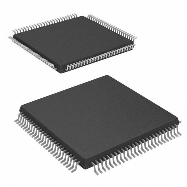


 工商网监
湘ICP备2023018690号
工商网监
湘ICP备2023018690号
