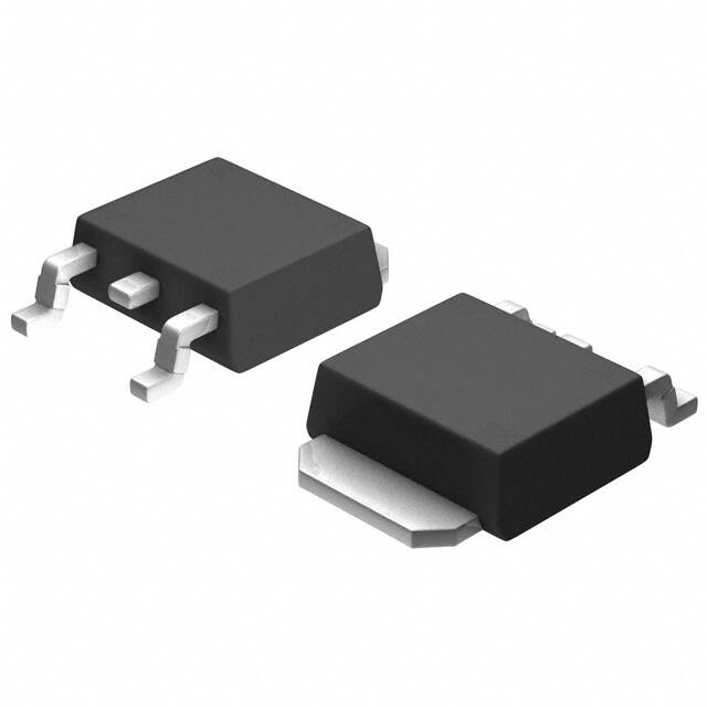
RGPZ10BM40FH
Datasheet
430V 20A Ignition IGBT
Outline
BVCES
43030V
IC
20A
VCE(sat) (Typ.)
1.6V
EAS
250mJ
TO-252
(2)
(1)
(3)
Features
Inner Circuit
1) Low Collector - Emitter Saturation Voltage
(2)
2) High Self-Clamped Inductive Switching Energy
3) Built in Gate-Emitter Protection Diode
(1) Gate
(2) Collector
(3) Emitter
(1)
4) Qualified to AEC-Q101
5) Pb - free Lead Plating ; RoHS Compliant
(3)
Packaging Specifications
Packaging
Applications
Ignition Coil Driver Circuits
Type
Solenoid Driver Circuits
Taping
Reel Size (mm)
330
Tape Width (mm)
16
Basic Ordering Unit (pcs)
Packing Code
2,500
TL
Marking
RGPZ10BM40
Absolute Maximum Ratings (at TC = 25°C unless otherwise specified)
Parameter
Symbol
Value
Unit
Collector - Emitter Voltage
VCES
460
V
Emitter-Collector Voltage (VGE = 0V)
VEC
25
V
Gate - Emitter Voltage
VGE
10
V
IC
20
A
EAS
250
mJ
150
mJ
Collector Current
Avalanche Energy (Single Pulse)
Tj = 25°C
Tj = 150°C
EAS
*2
Power Dissipation
PD
107
W
Operating Junction Temperature
Tj
40 to +175
°C
Tstg
55 to +175
°C
Storage Temperature
www.rohm.com
© 2015 ROHM Co., Ltd. All rights reserved.
1/8
2015.10 - Rev.A
�Data Sheet
RGPZ10BM40FH
Thermal Resistance
Parameter
Symbol
Rθ(j-c)
Thermal Resistance Junction - Case
Values
Min.
Typ.
Max.
-
-
1.40
Unit
°C/W
Electrical Characteristics (at Tj = 25°C unless otherwise specified)
Parameter
Symbol
Conditions
Values
Unit
Min.
Typ.
Max.
Tj = 25°C
400
430
460
V
Tj = 40 to 175°C*2
395
-
465
V
IC = 2mA, VGE = 0V
Collector - Emitter Breakdown
Voltage
BVCES
Emitter - Collector Breakdown
Voltage
BVEC
IC = 10mA, VGE = 0V
25
35
-
V
Gate - Emitter Breakdown
Voltage
BVGES
IG = 5mA, VCE = 0V
12
-
±17
V
Tj = 25°C
-
-
7
μA
Tj = 150°C*2
-
-
100
μA
VGE = 10V, VCE = 0V
-
-
15
μA
Tj = 25°C
1.3
1.7
2.1
V
Tj = 150°C
-
1.3
-
V
Tj = 25°C
-
1.60
2.00
V
Tj = 150°C
-
1.80
-
V
VCE = 300V, VGE = 0V
Collector Cut - off Current
Gate - Emitter Leakage Current
ICES
IGES
VCE = 5V, IC = 10mA
Gate - Emitter Threshold
Voltage
VGE(th)
IC = 10A, VGE = 5V
Collector - Emitter Saturation
Voltage
www.rohm.com
© 2015 ROHM Co., Ltd. All rights reserved.
VCE(sat)
2/8
2015.10 - Rev.A
�Data Sheet
RGPZ10BM40FH
Electrical Characteristics (at Tj = 25°C unless otherwise specified)
Parameter
Symbol
Conditions
Values
Unit
Min.
Typ.
Max.
Tj = 25°C
-
1.17
1.50
V
Tj = 150°C
-
1.13
-
V
Tj = 25°C
-
1.70
2.10
V
Tj = 150°C
-
1.90
-
V
IC = 4A, VGE = 4.5V
Collector - Emitter Saturation
Voltage
VCE(sat)
IC = 10A, VGE = 4V
Collector - Emitter Saturation
Voltage
VCE(sat)
Input Capacitance
Cies
VCE = 10V
-
1000
-
Output Capacitance
Coes
VGE = 0V
-
175
-
Reverse Transfer Capacitance
Cres
f = 1MHz
-
55
-
Total Gate Charge
Qg
VCE = 15V, IC = 10A,
VGE = 5V
-
14
-
0.09
0.17
0.50
0.10
0.18
0.50
0.8
1.3
4.0
Turn - on Delay Time*1,*2
Rise Time
*1,*2
Turn - off Delay Time
td(on)
tr
*1,*2
td(off)
IC = 8A, VCC = 300V,
VGE = 5V, RG = 100Ω,
L=5mH, Tj=25°C
pF
nC
μs
*1,*2
tf
1.4
2.4
6.0
Turn - on Delay Time*1
td(on)
-
0.16
-
-
0.23
-
-
1.5
-
-
3.9
-
250
-
-
mJ
150
-
-
mJ
70
100
130
Ω
Fall Time
*1
tr
Rise Time
Turn - off Delay Time
*1
Fall Time*1
td(off)
IC = 8A, VCC = 300V,
VGE = 5V, RG = 100Ω,
L=5mH, Tj=150°C
tf
μs
L = 5mH, VGE = 5V,
VCC = 30V, RG = 1kΩ,
Avalanche Energy (Single Pulse)
EAS
Tj = 25°C
Tj = 150°C
Gate Series Resistance
*2
RG
*1) Assurance items according to our measurement definition (Fig.16)
*2) Design assurance items
www.rohm.com
© 2015 ROHM Co., Ltd. All rights reserved.
3/8
2015.10 - Rev.A
�Data Sheet
RGPZ10BM40FH
Electrical Characteristic Curves
Fig.1 Typical Output Characteristics
30
30
Tj= 25ºC
VGE= 10V
VGE= 8V
VGE= 4V
VGE= 5V
20
TTj=j= 175ºC
25ºC
VGE= 4.5V
VGE= 3.5V
15
10
5
VGE= 8V
VGE= 5V
20
VGE= 4.5V
15
VGE= 4V
10
VGE= 3.5V
5
0
0
0
1
2
3
4
5
0
Collector To Emitter Voltage : VCE[V]
VGE= 3.5V
4V
4.5V
1.3
1.2
5V
1.1
8V
10V
1
25
50
75
Collector To Emitter Saturation Voltage
: VCE(sat) [V]
Collector To Emitter Saturation Voltage
: VCE(sat) [V]
2.3
1.4
100 125 150 175 200
3
4
5
IC= 10A
2.2
2.1
VGE= 3.5V
2
4V
1.9
4.5V
1.8
1.7
1.6
1.5
5V
1.4
8V
10V
1.3
0
Junction Temperature : Tj [ºC]
www.rohm.com
© 2015 ROHM Co., Ltd. All rights reserved.
2
Fig.4 Typical Collector To Emitter Saturation
Voltage vs. Junction Temperature
1.5
IC= 5A
1
Collector To Emitter Voltage : VCE[V]
Fig.3 Typical Collector To Emitter Saturation
Voltage vs. Junction Temperature
0
VGE= 10V
25
Collector Current : IC [A]
25
Collector Current : IC [A]
Fig.2 Typical Output Characteristics
25
50
75
100 125 150 175 200
Junction Temperature : Tj [ºC]
4/8
2015.10 - Rev.A
�Data Sheet
RGPZ10BM40FH
Electrical Characteristic Curves
Fig.5 Typical Collector To Emitter Saturation Voltage
vs. Junction Temperature
Fig.6 Typical Transfer Characteristics
20
VCE= 5V
VGE= 5V
2
IC= 10A
1.5
IC= 4.5A
1
IC= 1A
0.5
Collector Current : IC [A]
Collector To Emitter Saturation Voltage
: VCE(sat) [V]
2.5
15
10
5
Tj= 175ºC
0
0
0
25
50
75
100 125 150 175 200
0
Junction Temperature : Tj [ºC]
3
4
5
10000
VCE= 5V
IC= 10mA
1.9
1.7
1.5
1.3
1.1
0.9
Leakage Current : ICES/IEC [A]
Gate To Emitter Threshold Voltage
: VGE (th) [V]
2
Fig.8 Typical Leakage Current
vs. Junction Temperature
2.5
2.1
1
Gate To Emitter Voltage : VGE [V]
Fig.7 Typical Gate To Emitter Threshold Voltage
vs. Junction Temperature
2.3
Tj= 25ºC
1000
VEC= 25V
100
10
1
VCES= 300V
0.1
0.7
0.5
0.01
-50 -25 0
25 50 75 100 125 150 175 200
-50 -25 0
Junction Temperature : Tj [ºC]
www.rohm.com
© 2015 ROHM Co., Ltd. All rights reserved.
25 50 75 100 125 150 175 200
Junction Temperature : Tj [ºC]
5/8
2015.10 - Rev.A
�Data Sheet
RGPZ10BM40FH
Electrical Characteristic Curves
460
VGE= 0V
450
440
ICES= 2mA
430
420
410
400
-50 -25 0
Fig.10 Typical Self Clamped Inductive
Switching Current vs. Inductance
Self Clamped Inductive Switching Current
: IAS [A]
Collector To Emitter Breakdown Voltage
: BVCES [V]
Fig.9 Typical Collector To Emitter Breakdown
Voltage vs. Junction Temperature
40
VCC= 30V
VGE= 5V
RG= 1kΩ
35
30
25
20
15
10
5
0
0
25 50 75 100 125 150 175 200
1
Junction Temperature : Tj [ºC]
3
4
5
6
7
8
9
10
Inductance : L [mH]
Fig.11 Typical Gate Charge
Fig.12 Typical Capacitance
vs. Collector To Emitter Voltage
5
10000
4
Cies
1000
Capacitance [pF]
Gate To Emitter Voltage : VGE [V]
2
3
2
0
0
5
10
f= 1MHz
VGE= 0V
Tj= 25ºC
1
0.01
15
Gate Charge : Qg [nC]
www.rohm.com
© 2015 ROHM Co., Ltd. All rights reserved.
Coes
10
VCC= 12V
IC= 10A
Tj= 25ºC
1
100
0.1
Cres
1
10
100
Collector To Emitter Voltage : VCE[V]
6/8
2015.10 - Rev.A
�Data Sheet
RGPZ10BM40FH
Electrical Characteristic Curves
Fig.13 Typical Switching Time
vs. Junction Temperature
Switching Time [μs]
10
VCC= 30V, IC= 8A,
VGE= 5V, L= 5mH,
Rg= 100Ω
tf
td(off)
1
tr
td(on)
0.1
0
25
50
75
100 125 150 175 200
Junction Temperature : Tj [ºC]
Fig.14 Transient Thermal Impedance
Transient Thermal Impedance
: ZthJC [ºC/W]
10
D= 0.5
0.3
0.2
0.1
1
0.1
PDM
Single Pulse
0.02
0.01
0.01
0.05
0.001
0.00001
t1
C1
C2
C3
R1
R2
R3
1.472m 983.8u 3.844m 391.6m 985.3m 23.10m
0.0001
0.001
0.01
t2
Duty=t1/t2
Peak Tj=PDM×ZthJCTC
0.1
1
Pulse Width : t1[s]
www.rohm.com
© 2015 ROHM Co., Ltd. All rights reserved.
7/8
2015.10 - Rev.A
�Data Sheet
RGPZ10BM40FH
Inductive Load Switching Circuit and Waveform
Gate Drive Time
90%
VGE
10%
90%
IC
D.U.T.
10%
td(off)
td(on)
tf
tr
VG
toff
ton
VCE
Fig.15 Inductive Load Switching Circuit
VCE(sat)
Fig.16 Inductive Load Switching Waveform
Self Clamped Inductive Switching Circuit and Waveform
Vclamp
IC
D.U.T.
VCE
VCC
VCE(sat)
VG
EAS
Fig.17 Self Clamped Inductive Switching Circuit
www.rohm.com
© 2015 ROHM Co., Ltd. All rights reserved.
Fig.18 Self Clamped Inductive Switching Waveform
8/8
2015.10 - Rev.A
�Notice
Notes
1) The information contained herein is subject to change without notice.
2) Before you use our Products, please contact our sales representative and verify the latest specifications :
3) Although ROHM is continuously working to improve product reliability and quality, semiconductors can break down and malfunction due to various factors.
Therefore, in order to prevent personal injury or fire arising from failure, please take safety
measures such as complying with the derating characteristics, implementing redundant and
fire prevention designs, and utilizing backups and fail-safe procedures. ROHM shall have no
responsibility for any damages arising out of the use of our Poducts beyond the rating specified by
ROHM.
4) Examples of application circuits, circuit constants and any other information contained herein are
provided only to illustrate the standard usage and operations of the Products. The peripheral
conditions must be taken into account when designing circuits for mass production.
5) The technical information specified herein is intended only to show the typical functions of and
examples of application circuits for the Products. ROHM does not grant you, explicitly or implicitly,
any license to use or exercise intellectual property or other rights held by ROHM or any other
parties. ROHM shall have no responsibility whatsoever for any dispute arising out of the use of
such technical information.
6) The Products are intended for use in general electronic equipment (i.e. AV/OA devices, communication, consumer systems, gaming/entertainment sets) as well as the applications indicated in
this document.
7) The Products specified in this document are not designed to be radiation tolerant.
8) For use of our Products in applications requiring a high degree of reliability (as exemplified
below), please contact and consult with a ROHM representative : transportation equipment (i.e.
cars, ships, trains), primary communication equipment, traffic lights, fire/crime prevention, safety
equipment, medical systems, servers, solar cells, and power transmission systems.
9) Do not use our Products in applications requiring extremely high reliability, such as aerospace
equipment, nuclear power control systems, and submarine repeaters.
10) ROHM shall have no responsibility for any damages or injury arising from non-compliance with
the recommended usage conditions and specifications contained herein.
11) ROHM has used reasonable care to ensur the accuracy of the information contained in this
document. However, ROHM does not warrants that such information is error-free, and ROHM
shall have no responsibility for any damages arising from any inaccuracy or misprint of such
information.
12) Please use the Products in accordance with any applicable environmental laws and regulations,
such as the RoHS Directive. For more details, including RoHS compatibility, please contact a
ROHM sales office. ROHM shall have no responsibility for any damages or losses resulting
non-compliance with any applicable laws or regulations.
13) When providing our Products and technologies contained in this document to other countries,
you must abide by the procedures and provisions stipulated in all applicable export laws and
regulations, including without limitation the US Export Administration Regulations and the Foreign
Exchange and Foreign Trade Act.
14) This document, in part or in whole, may not be reprinted or reproduced without prior consent of
ROHM.
Thank you for your accessing to ROHM product informations.
More detail product informations and catalogs are available, please contact us.
ROHM Customer Support System
http://www.rohm.com/contact/
www.rohm.com
© 2015 ROHM Co., Ltd. All rights reserved.
R1102A
�