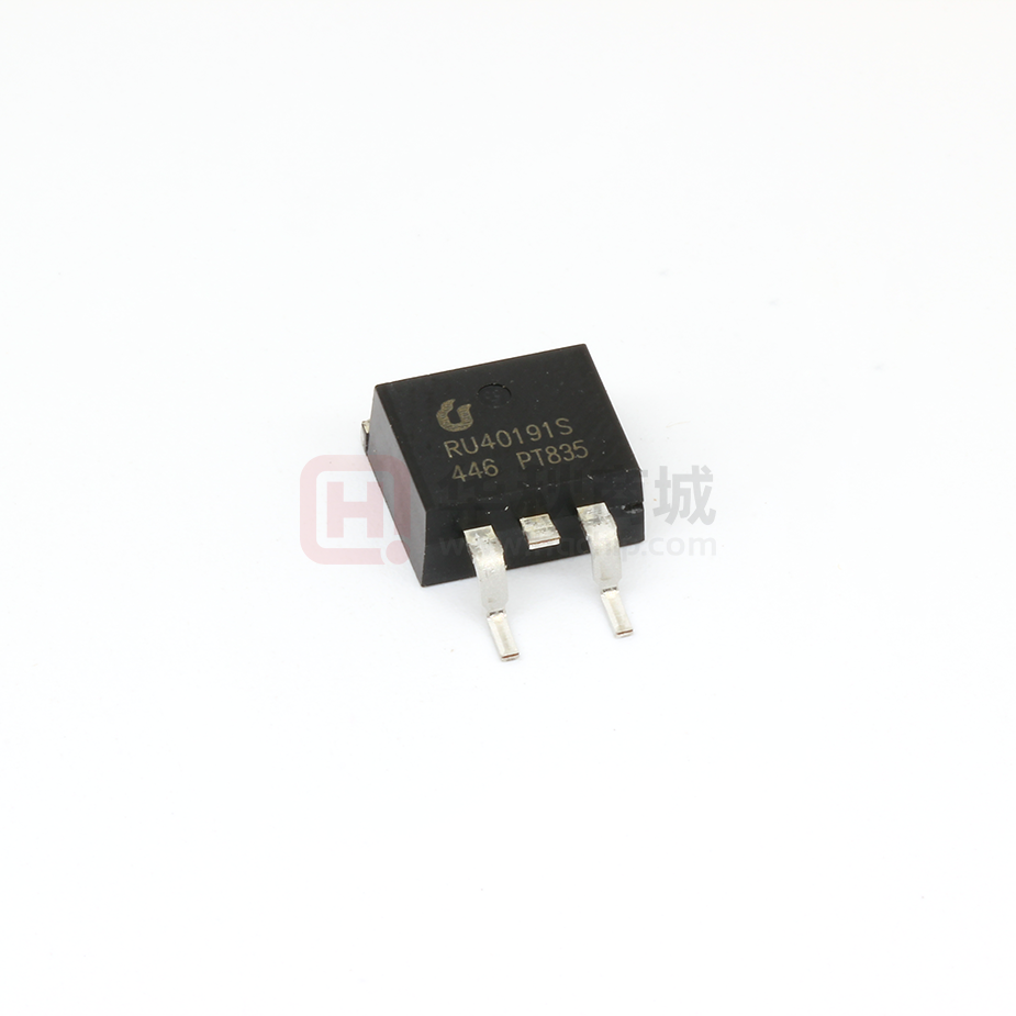
RU40191S
N-Channel Advanced Power MOSFET
Features
Pin Description
• 40V/190A,
RDS (ON) =1.8mΩ(Typ.)@VGS=10V
D
• Super High Dense Cell Design
• Ultra Low On-Resistance
• 100% avalanche tested
G
S
• Lead Free and Green Devices Available (RoHS Compliant)
TO263
D
Applications
• DC-DC Converters and Off-line UPS
• Switching Applications
G
S
N-Channel MOSFET
Absolute Maximum Ratings
Symbol
Parameter
Rating
Unit
Common Ratings (TC=25°C Unless Otherwise Noted)
VDSS
Drain-Source Voltage
40
VGSS
Gate-Source Voltage
±20
Maximum Junction Temperature
175
°C
-55 to 175
°C
TC=25°C
190
A
TC=25°C
760
A
TC=25°C
190
TC=100°C
146
TC=25°C
300
TC=100°C
150
TJ
TSTG
IS
Storage Temperature Range
Diode Continuous Forward Current
V
Mounted on Large Heat Sink
①
300μs Pulse Drain Current Tested
ID
②
Continuous Drain Current(VGS=10V)
PD
Maximum Power Dissipation
IDP
A
W
RqJC
Thermal Resistance-Junction to Case
0.5
°C/W
RqJA
Thermal Resistance-Junction to Ambient
62.5
°C/W
812
mJ
Drain-Source Avalanche Ratings
EAS
③
Avalanche Energy, Single Pulsed
Ruichips Semiconductor Co., Ltd
Rev. B– DEC., 2019
1
www.ruichips.com
�RU40191S
Electrical Characteristics (TC=25°C Unless Otherwise Noted)
Symbol
Parameter
Test Condition
RU40191S
Min.
Typ.
Max.
Unit
Static Characteristics
BVDSS
Drain-Source Breakdown Voltage
IDSS
Zero Gate Voltage Drain Current
VGS(th)
IGSS
④
RDS(ON)
VGS=0V, IDS=250µA
40
V
VDS=40V, VGS=0V
1
TJ=125°C
Gate Threshold Voltage
VDS=VGS, IDS=250µA
Gate Leakage Current
VGS=±20V, VDS=0V
Drain-Source On-state Resistance VGS=10V, IDS=75A
30
1
1.8
µA
3
V
±100
nA
3
mΩ
1.3
V
Diode Characteristics
VSD
④
Diode Forward Voltage
trr
Reverse Recovery Time
Qrr
Reverse Recovery Charge
ISD=75A, VGS=0V
ISD=75A, dlSD/dt=100A/µs
40
ns
52
nC
Ω
⑤
Dynamic Characteristics
RG
Gate Resistance
VGS=0V,VDS=0V,F=1MHz
1.2
Ciss
Input Capacitance
VGS=0V,
4800
Coss
Output Capacitance
950
Crss
Reverse Transfer Capacitance
VDS=20V,
Frequency=1.0MHz
td(ON)
Turn-on Delay Time
tr
Turn-on Rise Time
VDD=20V,IDS=75A,
96
td(OFF)
Turn-off Delay Time
VGEN=10V,RG=2.5Ω
70
tf
ns
50
⑤
Qg
Total Gate Charge
Qgs
Gate-Source Charge
Qgd
Gate-Drain Charge
Notes:
480
19
Turn-off Fall Time
Gate Charge Characteristics
pF
VDS=32V, VGS=10V,
IDS=75A
120
34
nC
46
①Pulse width limited by safe operating area.
②Calculated continuous current based on maximum allowable junction temperature. The package
limitation current is 75A.
③Limited by TJmax, IAS =57A, VDD = 32V, RG = 50Ω , Starting TJ = 25°C.
④Pulse test ; Pulse width≤300µs, duty cycle≤2%.
⑤Guaranteed by design, not subject to production testing.
Ruichips Semiconductor Co., Ltd
Rev. B– DEC., 2019
2
www.ruichips.com
�RU40191S
Ordering and Marking Information
Device
Marking
Package
RU40191S
RU40191S
TO263
Tube
50
-
-
RU40191S-R
RU40191S
TO263
Reel
800
13"
24mm
Ruichips Semiconductor Co., Ltd
Rev. B– DEC., 2019
Packaging Quantity Reel Size Tape width
3
www.ruichips.com
�RU40191S
Typical Characteristics
VGS=10V
RDS(ON) limited
Ids=75A
10µs
100µs
1ms
10ms
DC
TC=25°C
Duty=0.5, 0.2, 0.1, 0.05, 0.02, 0.01, Single Pulse
Single Pulse
RθJC=0.5°C/W
Ruichips Semiconductor Co., Ltd
Rev. B– DEC., 2019
4
www.ruichips.com
�RU40191S
Typical Characteristics
VGS=8,9,10V
5V
10V
3V
VGS=10V
IDS=75A
TJ=150°C
TJ=25°C
TJ=25°C
Rds(on)=1.8mΩ
Frequency=1.0MHz
VDS=32V
IDS=75A
Ciss
Coss
Crss
Ruichips Semiconductor Co., Ltd
Rev. B– DEC., 2019
5
www.ruichips.com
�RU40191S
Avalanche Test Circuit and Waveforms
Switching Time Test Circuit and Waveforms
Ruichips Semiconductor Co., Ltd
Rev. B– DEC., 2019
6
www.ruichips.com
�RU40191S
Package Information
TO263
θ1
θ1
θ2
θ
θ2
Ruichips Semiconductor Co., Ltd
Rev. B– DEC., 2019
7
www.ruichips.com
�
